 Open Access Article
Creative Commons Attribution 3.0 Unported Licence
Morphology and electrical characteristics of p-type ZnO microwires with zigzag rough surfaces induced by Sb doping†
Linlin Shi a,
Luchao Duc,
Yingtian Xua,
Liang Jina,
He Zhanga,
Yan Lia,
Xiaohui Maa,
Yonggang Zou
 *a and
Dongxu Zhaob
aState Key Laboratory of High Power Semiconductor Laser, Changchun University of Science and Technology, No. 7186 Wei-Xing Road, Changchun, 130022, People's Republic of China. E-mail: zouyg@cust.edu.cn; Fax: +86-85583395; Tel: +86-85583395
bState Key Laboratory of Luminescence and Applications, Changchun Institute of Optics, Fine Mechanics and Physics, Chinese Academy of Sciences, No. 3888 Dongnanhu Road, Changchun, 130033, People's Republic of China
cInstitute of Atomic and Molecular Physics, Jilin University, No. 2699 Qian-Jin Road, Changchun, 130012, People's Republic of China
First published on 12th October 2018
Abstract
Sb-doped p-type ZnO microwires with zigzag rough surfaces were synthesized by two zone chemical vapor deposition. The zigzag morphology characteristics analyzed by high resolution scanning electron microscopy and transmission electron microscopy show the existence of surface defects caused by Sb doping. The incorporation of Sb into a ZnO lattice induces lattice imperfection, which is the origin of the zigzag rough surface. Photoluminescence and electrical properties of the obtained Sb-doped ZnO microwires were determined. The crossed structure microwire-based p–n homojunction device was fabricated by applying as-synthesized Sb-doped p-type ZnO microwires and undoped n-type ZnO microwires. The doped microwires demonstrate reproducible p-type conduction and enhanced rectifying behavior with increasing Sb doping concentration. The results demonstrated that the optimizable optical and electrical characteristics, controlled by increasing the doping concentration, are reflected in the surface morphology changes which would be helpful for characterizing the doping effects in micro/nanoscale materials.
Introduction
Single crystalline metal oxide semiconductor micro/nanomaterials have been utilized as building blocks in many photonic and electronic applications.1–3 Because of their superior properties, such as multi-functionality, high crystallinity, quantum size effects, high transparency, and stability in air, micro/nanomaterials can act as future electronic material alternatives to bulk materials. ZnO is one of the promising materials for the fabrication of optoelectronic devices operating in the blue and ultraviolet regions because of the wide direct band gap (3.37 eV) and large exciton binding energy (60 mV).4,5 p-Type doping in ZnO is essential for device applications to meet the increasing needs of present applications, and enormous efforts have been dedicated to the doping of ZnO with selective elements to fabricate homojunction devices, which have the advantages of high sensitivity, fast response speed, and high stability in various environments.6,7 However reports based on the homojunction devices of ZnO nanostructure are relatively rare; stable and reproducible p-type doping of ZnO is still a great challenge.8–11 Much effort has been made to obtain high quality p-type ZnO, it had been reported that Sb element with a large atom size is a good choice of ZnO dopant.12–14 Sb atom would substitute for a Zn atom and simultaneously produce two corresponding Zn vacancies, therefore Sb-doped ZnO shows strong p-type conduction based on first-principles calculation,15 hence large-mismatched Sb atoms are efficient p-type dopants for ZnO nanowires.16–18Recently, various synthesis methods have been developed to synthesize micro/nanomaterials with controlling of their size and shape, including both vapor phase and solution phase synthesis, to enhance the multi-functionality of ZnO in different application fields.19,20 ZnO microwires with a novel square cross-section have promising prospect in the field of cavity quantum electrodynamics and the development of miniature optoelectronic devices.21,22 The electrical, optical, and magnetic properties of ZnO nanostructures can be drastically modified by impurity doping.23,24 Moreover, more complex ZnO structures can be developed when impurities are mixed into the source material. Some researchers reported that Sb in ZnO have an effect on the morphology of nanostructure.25–27 The introduction of Sb can alter the morphology of the ZnO nanomaterials, including crystal size, orientation, and aspect ratio, which also have important effects on their electrical and optical properties, gas sensitivity and catalytic properties.28 When Sb was introduced into ZnO, it has higher resistance and diffuse reflectivity than those of the undoped ZnO. But to our knowledge, there is no report concerning p-type conduction properties affected by morphology variation in Sb-doped ZnO.
Furthermore, micro/nanowires with 1D nanostructure have promising applications in developing novel devices. Novel devices constructed by two crossed micro/nanowire components to create efficient nanoscale p–n junction diodes have been previously configured as diodes successfully.29,30 The ability to fabricate micro/nanowire heterostructures should further increase the versatility of nanowire based electronic and photonic devices and also provide convenient subsequent assembly processes.31,32
In this study, ultralong Sb-doped ZnO single crystalline microwires were synthesized by vapor phase synthesis, the obtained Sb-doped ZnO microwire showed high crystalline in both zigzag surface area and inside area. P-type properties of ZnO microwires were examined by photoluminescence and electrical measurements, and the morphology and electrical properties changes with the concentration of Sb-doping. The crossed p–n homojunction was fabricated to identify p-type properties of zigzag by crossing a single Sb-doped ZnO microwire and a single undoped ZnO microwire.
Results and discussion
Morphologies and characterization
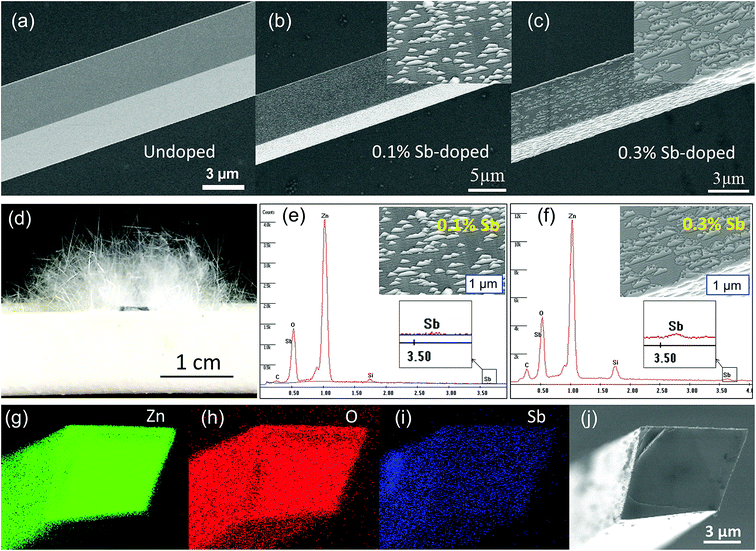
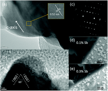
The as-synthesized ZnO microwire was analysed by Scanning Electron Microscope (SEM) to demonstrate the structural characters. The morphologies of both undoped and Sb-doped ultralong ZnO microwires with square cross-section are revealed in Fig. 1a–c. The surface morphology changes distinctly due to the incorporation of the Sb dopant, the microwire presents a zigzag rough surface compared to the smooth surface of the undoped ZnO microwire. Fig. 1d displays optical imaging of the as synthesized ultralong ZnO microwires on an alumina boat, the length can reach to about 10 millimeters. To determine the composition of Sb in ZnO microwires, we performed the Energy Dispersive X-ray spectroscopy (EDX) composition analysis taken in various regions to investigate Sb and Zn distribution. The morphology variation was investigated, it changes with the concentration of the Sb element in the microwire, Sb concentration was 0.1% and 0.3% in Sb-doped microwires within the measurement limit of EDX. The surface of zigzag roughness increases with the doping concentration, the details are shown from the inset enlarged SEM image in Fig. 1e and f. With the increase of doping concentration, triangle embossment became intensively and obviously in 0.3% Sb-doped microwire. To further confirm the existence of Sb-doping, the cross section element mappings of individual Sb-doped ZnO microwires using EDX are depicted in Fig. 1g–j. Zn, O and Sb are homogeneously and uniformly distributed in the microwires. The inset is the local magnified portion with the energy from about 4 keV to 6 keV, indicating the existence of Sb in the doped material.To understand the origin of the novel zigzag surfaces in the microwires, the corresponding magnification of triangle edges of the Sb-doped ZnO microwire were further determined by high-resolution TEM and SEM analysis. The results are recorded in Fig. 2. Detailed information can be obtained from the clear lattice structure, indicate good crystal quality. The c-axis growth direction with d-spacing of 0.52 nm was indicated by adjacent lattice spacing, it can be indexed into [0001] growth orientation, which is the favoured growth direction of ZnO microwire. The angle measurement of edges with respect to the [002] direction revealed an angle of ∼60° between the two planar defects,25 which is consistent with the angle relationship between the (010) and (002) planes in the SAED pattern.33 The corresponding selected area electron diffraction (SAED) pattern in Fig. 2c reveals that the growth orientations is along [0001]. The internal structures of the Sb-doped ZnO microwires were further characterized by enlarged SEM characterizations of triangle zone of microwire surface which are shown in Fig. 2d and e. The enlarged images of the edges of ZnO microwire display a smooth transition of the edges of ZnO display a smooth transition between the zigzag surface and internal microwire, both in 0.1% Sb-doped (Fig. 2d) and 0.3% Sb-doped (Fig. 2e) microwire. The above results reveal that Sb-doped ZnO microwires were highly crystallized with zigzag surface.
The origination of the zigzag rough surface in ZnO microwires could be attributed to the introduction of Sb dopants. Sb element is responsible for the formation of the single-side zigzag boundaries in the nanowires, the radius of Sb3+ (0.078 nm) is much larger than that of Zn2+ (0.074 nm), the introduction of Sb3+ ions should cause a large structural strain. Since the radius of Sb3+ (0.78 Å) is much larger than that of Zn2+ (0.74 Å), the introduction of Sb atoms would cause a large structural strain, the release of the structural strain could result in the formation of the planar defects.34 When Sb in ZnO, the surface energy of (001) planes is reduced, crystal growth along the (001) orientation is suppressed, and then the morphology of the ZnO micro/nanowires can be changed. ZnO microwires usually grow along the c axis, and the side surfaces are {0110} and/or {2110} because of the lower energy surfaces compared to (0001).25 The solutes prefer to segregate from the host and occupy the surface of the nanostructures, result in a decreased surface energy.26 Hence we propose that Sb is responsible for the zigzag surface and zigzag shaped microwires are surrounded by (0002), (0110) and (2110) as the surface.27
Growth mechanism
In our experiment, the doping procedure performed under the two zone in situ synthesis condition, the synthesis condition is shown in Fig. 3. The Sb source served as the dopant source material could vaporize at the same speed with Zn source. When the substrate was heated to about 1100 °C, oxygen was introduced for about 2 min to keep the synthesis under the oxygen-rich conditions which would suppress the formation of SbO. The rough surface morphologies become obviously with increasing the O2 flow, which is shown in Fig. S1.† Based on the above experimental process and relevant analyses, we proposed the growth mechanism of the doping procedure of in situ doping of Sb-doped ZnO microwire, the schematic diagram is shown in Fig. 3a. The reaction temperature of Sb source (Sb2O3 powder) is about 600 °C, which is much lower than the synthesis temperature of ZnO. By separating two heating zones, Zn and Sb vapor was generated simultaneously to the growth substrate with the temperature increasing, deposited on the growth substrate to form droplets. As the O2 gas was introduced into the furnace at 1100 °C, when the ZnO in the droplets reach a saturated concentration, Sb-doped crystalline ZnO begin to grow from the droplets. The initially formed Sb vapor from the source can provide the necessary feeding dopant material for the microwire growth. It suggests that Sb vapor is diffused full of the whole growth process, the surface zigzag morphology affected by the inside defect could contribute to the introduction of Sb atoms in the ZnO crystal growth process.24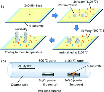 | ||
| Fig. 3 (a) Schematic diagram of the growth process of the Sb-doped ZnO microwire, (b) schematic diagram of the two zone growth condition. | ||
Optical properties
To investigate optical properties of the ZnO microwires, photoluminescence (PL) spectra were measured at room temperature using the 325 nm line of a He–Cd laser as an excitation source, the results are shown in Fig. 4a. As can be seen from the PL spectra, the near-band edge (NBE) emission centered at 382 nm can be mainly observed in both undoped and Sb-doped ZnO microwires, there are two emission peaks in Sb-doped ZnO microwires with an ultraviolet (UV) emission related to the NBE attributed to the exciton recombination of ZnO, and a broad green emission band related to defects at centered at 500 nm in both 0.1% and 0.3% Sb-doped microwires. The broad visible emission can be identified as deep level defects which usually caused by impurities and structural defects.35 According to the normalized PL spectrum in Fig. 4a, the intensity ratios of the visible emission to the UV emission of 0.3% Sb-doped microwire is larger than 0.1% Sb-doped microwire, the increasing defect emission peak could be result from the introducing of increased impurity atoms, indicates the decreased crystallinity of the zigzag ZnO nanostructure and effective Sb defects inside. Compared with the undoped ZnO microwire, the intrinsic emission of 0.3% doped microwire is at 377.37 nm (3.26 eV), with a marked deviation of 0.085 eV from the emission (387.65 nm, 3.19 eV) of undoped ZnO. For 0.1% Sb-doped microwire (384.04 nm, 3.23 eV), the deviation is 0.04 eV, which is smaller than the 0.3% Sb-doped microwire. This is probably due to the formation of acceptor levels by Sb doping. With the doping concentration increases, the intensity of defect emission peak increases and the zigzag rough surfaces become obvious.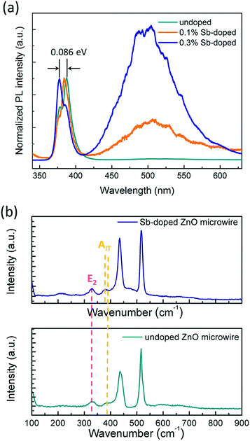 | ||
| Fig. 4 (a) Normalized photoluminescence of Sb-doped and undoped ZnO microwires at room temperature, (b) Raman spectra of Sb-doped and undoped ZnO microwires. | ||
The microstructure characterization and the optical property of the microwires were also investigated by the Raman scattering to further confirm the incorporation of Sb atoms into the ZnO microwire lattices. As shown in Fig. 4b, the peak centered at 436 cm−1 is usually attributed to the E2 modes of the undoped ZnO single crystal, and this peak shifts toward lower frequency to 434 cm−1 when doping with Sb, which is caused by the formation of the SbZn–2VZn low formation energy complex acceptor in Sb-doped ZnO microwires, the defect can be identified as represented the shallow acceptor defect levels.34,36 The peak at 380 cm−1 corresponds to the A1T modes in ZnO is depressed by Sb doping. Since the oxygen defect or the dopant atom directly affects the A1T modes, indicates that Sb dopant atoms would be responsible for the depression in 380 cm−1.37 Consequently, PL and Raman spectra characteristics reveal that Sb was incorporated into ZnO crystal lattices and the zigzag morphology have an impact on the emission according to Sb doping.
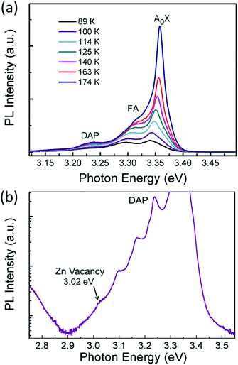
The p-type behaviour of the nanowires can also be confirmed optically by low-temperature photoluminescence (PL). The low-temperature (at 85 K) PL spectra of Sb-doped ZnO microwires were shown in Fig. 5a. The Sb-doped ZnO microwire spectrum shows a dominated emission peak centered at 3.354 eV, which is associated with the neutral-acceptor-bound exciton (A0X) recombination.38 The emission peaks located at 3.296 eV and 3.226 eV are ascribed to the free electron to acceptor (FA) and donor–acceptor-pair (DAP) transitions, respectively.39 The PL analysis suggests that the Sb-doped ZnO has shallow acceptor induced energy levels, which result in the p-type behavior of the microwires. The acceptor binding energy of EA in ZnO can be estimated by the following formula:
 | (1) |
Electrical properties
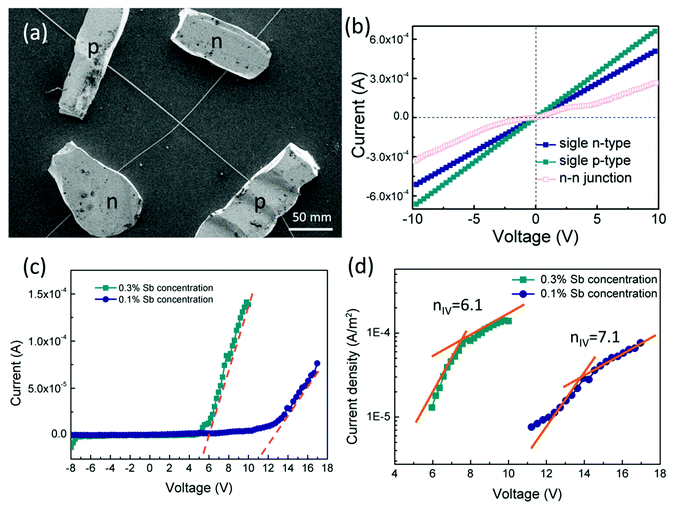
To confirm p-type conductance behaviour, a microwire-based p–n homojunction were fabricated with a single Sb doped p-type ZnO microwire and a single undoped n-type ZnO microwire, microwires were placed overlapping with each other on the glass substrate to form a crossed structure, fixed with indium electrodes at each end to create a crossed architecture. The crossed architecture is a clear example since the key device properties are defined by assembly of the two microwire components, and have the advantage of easy fabrication.41,42 The SEM image of the crossed heterojunction is shown in Fig. 6. Two metal–semiconductor (MS) contacts were used for two electrodes, MS contacts have been found to have dominative influence on the transport behavior of 1D nanomaterials, so the individual microwires with MS contacts were tested, the results are shown in Fig. 6b. Transport data recorded on the individual p-type and n-type ZnO microwires both exhibit linear behaviors, indicate that individual microwires form an ohmic contact with the electrodes. Current–voltage (I–V) data for the crossed p–n junction (Fig. 6c and d) shows well-defined current rectification. Transport measurement carried out on the n–n junction by crossing two n-type ZnO microwires shows nearly linear behaviour, which indicates that the interface between individual n-type microwires does not produce a nonlinear curve. Consequently, the rectification can be definitely attributed to the crossed p–n homojunction. The p–n homojunction diode with a turn-on voltage of approximately 10 V in 1% Sb-doped microwire and 5 V in 3% Sb-doped microwire, which showed enhanced rectifying behaviour by increasing Sb doping concentration. The crossed p–n homojunction exhibits a rectifying behavior with a lower turn-on voltage tuned by increasing Sb dopant concentration is resulted from the Sb inducement. The initial turn-on voltage is approximate to the bandgap of ZnO, corresponds to injection of electrons into the p-ZnO from the n-ZnO. According to the IV characteristics of the real diodes,43
 | (2) |
 | (3) |
![[thin space (1/6-em)]](https://www.rsc.org/images/entities/char_2009.gif) I–V characteristics.
I–V characteristics.
According to the Sah–Noyce–Shockley theory, the value of the ideality factor in a p–n junction is about 1.0–2.0 at low or high voltage. However, the value of n for the ZnO p–n homojunction is higher than the ideal diode according to the equation and Fig. 6, this may result from the presence of nonlinear MS contact in the system and in the junction area.44 The basal diode can be modeled by a series of resistances in a dissimilar bias voltage range. The substitution of Sb into ZnO contributes acceptor characteristics, the electrons in the outer shell of Sb should be taken into account, the outer shell d states generally appear near the Fermi level. The bonding states have a higher energy level and are very close to the conduction band, and the electrons in this state have a higher probability of jumping to the conduction band, resulting in the increase of conductivity with the increase of Sb concentration in ZnO, which cause the increase of the turn-on voltage of p–n junction semiconductor diode.
Conclusion
Sb-doped p-type ZnO microwires were synthesized by a CVD method, the morphology changed distinctly due to Sb incorporation. P-type properties of ZnO microwires were examined by photoluminescence and electrical measurements. Low-temperature PL and Raman spectra measurements showed that shallow acceptor was formed in the Sb-doped ZnO microwire. Fine rectification character was obtained on the crossed ZnO microwire p–n homojunction indicating the p-type conductivity of the Sb-doped ZnO microwire. The morphology and electrical properties changes with Sb-doping. The doped microwires demonstrate reproducible p-type conduction and enhanced rectifying behavior with increasing Sb doping concentration. The zigzag shape of ZnO microwires after introducing dopant could be a reflection of effective doping, the capability of testing p-type conduction characteristics and the understanding of emission behaviour of Sb-doped ZnO microwires have promising future applications of ZnO micro/nanowire based electronic and optoelectronic devices.Experimental
Synthesis of ZnO microwire
Sb-doped ZnO microwires were grown by a catalyst-free chemical vapor deposition (CVD) method with a two-zone tube furnace. ZnO and graphite powders were thoroughly mixed with a weight ratio of 1![[thin space (1/6-em)]](https://www.rsc.org/images/entities/char_2009.gif) :
:![[thin space (1/6-em)]](https://www.rsc.org/images/entities/char_2009.gif) 1, then the mixture was put into an alumina boat to act as the reactant source material. The Sb2O3 powders which served as the dopant source material were loaded into another boat at the upstream to ensure that Sb2O3 and ZnO powders could vaporize at the same speed. A 100 nm ZnO film was deposited on the Si substrate by the sputtering method, and then the substrate was loaded above the ZnO powders. During the synthesis progress, the two sources were loaded into the furnace at different temperature zones with a constant flow of 100 sccm argon (99.99%) as the carrier gas. The reactant ZnO source was heated to 1100 °C and the Sb2O3 dopant source was heated to 600 °C, simultaneously. When the ZnO source was heated to about 1100 °C, oxygen was introduced with a 20 sccm flow rate for about 2 min to keep the synthesis under the oxygen-rich conditions which would suppress the formation of VO and SbO. After maintaining the source temperature for 40 min, the furnace was turned off and cooled down to room temperature. The synthesis of the undoped ZnO microwires follows the same procedure without the Sb dopant source.
1, then the mixture was put into an alumina boat to act as the reactant source material. The Sb2O3 powders which served as the dopant source material were loaded into another boat at the upstream to ensure that Sb2O3 and ZnO powders could vaporize at the same speed. A 100 nm ZnO film was deposited on the Si substrate by the sputtering method, and then the substrate was loaded above the ZnO powders. During the synthesis progress, the two sources were loaded into the furnace at different temperature zones with a constant flow of 100 sccm argon (99.99%) as the carrier gas. The reactant ZnO source was heated to 1100 °C and the Sb2O3 dopant source was heated to 600 °C, simultaneously. When the ZnO source was heated to about 1100 °C, oxygen was introduced with a 20 sccm flow rate for about 2 min to keep the synthesis under the oxygen-rich conditions which would suppress the formation of VO and SbO. After maintaining the source temperature for 40 min, the furnace was turned off and cooled down to room temperature. The synthesis of the undoped ZnO microwires follows the same procedure without the Sb dopant source.
Measurements
The morphology of the ZnO microwires was characterized by a field-emission scanning electron microscope (FE-SEM) (model: Hitachi S-4800) equipped with an X-ray energy dispersive spectrometer (EDX). The selected area electron diffraction (SAED) patterns were obtained on a JEOL JEM-2100F. Photoluminescence (PL) measurement was carried out with a JY-630 micro-Raman spectrometer employing the 325 nm line of a He–Cd laser as the excitation source, and the room temperature Raman spectra were recorded using the same micro-Raman spectrometer with a 488 nm excitation source. The current–voltage characteristics of the crossed p–n homojunction device were measured using a Keithley 2611A measurement system.Conflicts of interest
There are no conflicts to declare.Acknowledgements
This work is supported by the National Natural Science Foundation of China (No. 61804013, 61804014, 61805023 and 21707010), and The Excellent Youth Foundation of Jilin Province under Grant No. 20180520194JH.Notes and references
- Y. Huang, X. F. Duan and C. M. Lieber, Small, 2005, 1, 142–147 CrossRef CAS PubMed.
- Y. Li, F. Qian, J. Xiang and C. M. Lieber, Mater. Today, 2006, 9, 18–27 CrossRef CAS.
- C. M. Lieber and Z. L. Wang, MRS Bull., 2007, 32, 99–108 CrossRef CAS.
- S. Chu, G. P. Wang, W. H. Zhou, Y. Q. Lin, L. Chernyak, J. Z. Zhao, J. Y. Kong, L. Li, J. J. Ren and J. L. Liu, Nat. Nanotechnol., 2011, 97, 1–5 Search PubMed.
- X. L. Ren, X. H. Zhang, N. S. Liu, L. Wen, L. W. Ding, Z. W. Ma, J. Su, L. Y. Li, J. B. Han and Y. H. Gao, Adv. Funct. Mater., 2015, 25, 2182–2188 CrossRef CAS.
- X. L. Ren, X. H. Zhang, N. S. Liu, L. Wen, L. W. Ding, Z. W. Ma, J. Su, L. Y. Li, J. B. Han and Y. H. Gao, Adv. Funct. Mater., 2015, 25, 2182–2188 CrossRef CAS.
- G. H. He, M. M. Jiang, B. H. Li, Z. Z. Zhang, H. F. Zhao, C. X. Shan and D. Z. Shen, J. Mater. Chem. C, 2017, 5, 10938–10946 RSC.
- Y. H. Leung, Z. B. He, L. B. Luo, C. H. Tsang and N. B. Wong, Appl. Phys. Lett., 2010, 96, 053102 CrossRef.
- J. Huang, S. Chu, J. Y. Kong, L. Zhang, C. M. Schwarz, G. P. Wang, L. Chernyak, Z. H. Chen and J. L. Liu, Adv. Opt. Mater., 2013, 1, 179–185 CrossRef.
- Y. M. Wang, Y. Chen, W. Q. Zhao, L. W. Ding, L. Wen, H. X. Li, F. Jiang, J. Su, L. Y. Li, N. S. Liu and Y. H. Gao, Nano-Micro Lett., 2017, 9, 11 CrossRef.
- H. D. Zhang, M. Yu, J. C. Zhang, C. H. Sheng, X. Yan, W. P. Han, Y. C. Liu, S. Chen, G. Z. Shen and Y. Z. Long, Nanoscale, 2015, 7, 10513–10518 RSC.
- M. T. Chen, M. P. Lu, Y. J. Wu, J. h. Song, C. Y. Lee, M. Y. Lu, Y. C. Chang, L. J. Chou, Z. L. Wang and L. J. Chen, Nano Lett., 2010, 10, 4387–4393 CrossRef CAS PubMed.
- G. D. Yuan, W. J. Zhang, J. S. Jie, X. Fan, J. A. Zapien, Y. H. Leung, L. B. Luo, P. F. Wang, C. S. Lee and S. T. Lee, Nano Lett., 2008, 8, 2591–2597 CrossRef CAS PubMed.
- W. Liu, F. X. Xiu, K. Sun, Y. H. Xie, K. L. Wang, Y. Wang, J. Zou, Z. Yang and J. L. Liu, J. Am. Chem. Soc., 2010, 132, 2498–2499 CrossRef CAS PubMed.
- J. K. Liang, H. L. Su, P. Y. Chuang, C. L. Kuo, S. Y. Huang, T. S. Chan, Y. C. Wu and J. C. A. Huang, Appl. Phys. Lett., 2015, 106, 212101 CrossRef.
- F. Nagasaki, T. Shimogaki, T. Tanaka, T. Ikebuchi, T. Ueyama, Y. Fujiwara, M. Higashihata, D. Nakamura and T. Okada, Jpn. J. Appl. Phys., 2016, 55, 08RE07 CrossRef.
- S. B. Bashar, M. Suja, M. Morshed, F. Gao and J. L. Li, Nanotechnology, 2016, 27, 065204 CrossRef PubMed.
- S. D. Baek, P. Biswas, J. W. Kim, Y. C. Kim, T. I. Lee and J. M. Myoung, ACS Appl. Mater. Interfaces, 2016, 8, 13018–13026 CrossRef CAS PubMed.
- Y. Cai, R. Kozhummal, C. Kubel, V. Trouillet, M. Bruns, S. Gutsch, M. Zachariasb and Y. Yang, J. Mater. Chem. A, 2017, 5, 14397–14405 RSC.
- F. Xu, Y. N. Lu, L. T. Sun and L. J. Zhi, Chem. Commun., 2010, 46, 3191–3193 RSC.
- Y. Liu, H. X. Dong, S. L. Sun, W. H. Liu, J. X. Zhan, Z. H. Chen, J. Wang and L. Zhang, Nanoscale, 2013, 5, 4123–4128 RSC.
- L. L. Shi, F. Wang, B. H. Li, X. Chen, B. Yao, D. X. Zhao and D. Z. Shen, J. Mater. Chem. C, 2014, 2, 5005–5010 RSC.
- M. Y. Lu, H. Y. Chen, C. Y. Tsai, Y. T. Tseng, Y. T.Kuo, H. C. Wang and M. P. Lu, Chem. Commun., 2016, 52, 12853–12856 RSC.
- Y. Liu, H. X. Dong, J. Lu, J. X. Zhan, J. Z. Li, Z. H. Chen and L. Zhang, Adv. Opt. Mater., 2014, 2, 1090–1097 CrossRef CAS.
- Y. Yang, J. J. Qi, Q. L. Liao, Y. Zhang, L. D. Tang and Z. Qin, J. Phys. Chem. C, 2008, 112, 17916–17919 CrossRef CAS.
- B. C. Cheng, B. X. Tian, W. Sun, Y. H. Xiao, S. J. Lei and Z. G. Wang, J. Phys. Chem. C, 2009, 113, 9638–9643 CrossRef CAS.
- L. Wang, K. Z. Chen and L. F. Dong, J. Phys. Chem. C, 2010, 114, 17358–17361 CrossRef CAS.
- D. G. Xiang, J. Su, A. Q. Zhang, Y. H. Gao, X. Y. Han, M. Sun, X. H. Zhang, G. Z. Shen, L. Jin and J. B. Wang, J. Nanosci. Nanotechnol., 2010, 10, 6629–6633 CrossRef CAS PubMed.
- K. G. Kim, T. H. Moon, J. Y. Kim and S. S. Kim, Nanotechnology, 2011, 22, 245203 CrossRef PubMed.
- K. G. Kim, J. M. Kang, M. W. Lee, C. J. Yoon, K. G. Cho and S. S. Kim, J. Appl. Phys., 2010, 49, 06GG05 Search PubMed.
- R. Agarwal and C. M. Lieber, Appl. Phys. A, 2006, 85, 209–215 CrossRef CAS.
- Y. M. Wang, Y. Chen, W. Q. Zhao, L. W. Ding, L. Wen, H. X. Li, F. Jiang, J. Su, L. Y. Li, N. S. Liu and Y. H. Gao, Nano-Micro Lett., 2017, 9, 11 CrossRef.
- G. Milano, L. D'Ortenzi, K. Bejtka, L. Mandrile, A. M. Giovannozzi, L. Boarino, C. F. Pirri, C. Ricciardi and S. Porro, J. Phys. Chem. C, 2018, 122, 8011–8021 CrossRef CAS.
- S. Limpijumnong, S. B. Zhang, S. H. Wei and C. H. Park, Phys. Rev. Lett., 2004, 92, 155504 CrossRef PubMed.
- B. C. H. Zang, J. F. Su, B. Wang, D. M. Zhang and Y. S. Zhang, J. Lumin., 2011, 13, 1817–1820 CrossRef.
- K. Samanta, P. Bhattacharya and R. S. Katiyar, J. Appl. Phys., 2010, 108, 113501 CrossRef.
- I. A. Palani, K. Okazaki, D. Nakamura, K. Sakai, M. Higashihata and T. Okada, Appl. Surf. Sci., 2012, 258, 3611–3616 CrossRef CAS.
- E. Przeździecka, E. Kamińska, I. Pasternak, A. Piotrowska and J. Kossut, Phys. Rev. B: Condens. Matter Mater. Phys., 2007, 76, 193303 CrossRef.
- K. Samanta, A. K. Arora, S. Hussain, S. Chakravarty and R. S. Katiyar, Curr. Appl. Phys., 2012, 12, 1381–1385 CrossRef.
- F. X. Xiu, Z. Yang, L. J. Mandalapu, D. T. Zhao and J. L. Liu, Appl. Phys. Lett., 2005, 87, 252102 CrossRef.
- M. Ding, Z. Guo, L. Q. Zhou, X. Fang, L. L. Zhang, L. Y. Zeng, L. N. Xie and H. B. Zhao, Crystals, 2018, 8, 223 CrossRef.
- D. Panda and T. Y. Tseng, J. Mater. Sci., 2013, 48, 6849–6877 CrossRef CAS.
- C. X. Wang, G. W. Yang, H. W. Liu, Y. H. Han, J. F. Luo, C. X. Gao and G. T. Zou, Appl. Phys. Lett., 2004, 84, 2427 CrossRef CAS.
- G. X. Zhu, Y. J. Liu, C. Zhang, Z. l. Zhu and Z. Xu, Chem. Lett., 2010, 39, 994–995 CrossRef CAS.
Footnote |
| † Electronic supplementary information (ESI) available. See DOI: 10.1039/c8ra07135g |
| This journal is © The Royal Society of Chemistry 2018 |

