 Open Access Article
Creative Commons Attribution 3.0 Unported Licence
Structure and optical properties of sputter deposited pseudobrookite Fe2TiO5 thin films
Hai Dang
Ngo†
 ab,
Thien Duc
Ngo†
 ab,
Akemi
Tamanai
 ac,
Kai
Chen
 ad,
Nguyen Thanh
Cuong
 e,
Orjan S.
Handegard
 ab,
Annemarie
Pucci
 c,
Naoto
Umezawa
 af,
Toshihide
Nabatame
 ag and
Tadaaki
Nagao
 *ab
*ab
aInternational Center for Materials Nanoarchitectonics, National Institute for Materials Science, Tsukuba 305-0044, Japan. E-mail: NAGAO.Tadaaki@nims.go.jp
bDepartment of Condensed Matter Physics, Graduate school of Science, Hokkaido University, Kita-10 Nishi-8 Kita-ku, Sapporo 060-0810, Japan
cHeidelberg University, Kirchhoff Institute for Physics, Im Neuenheimer Feld 227, 69120 Heidelberg, Germany
dInstitute of Photonics Technology, Jinan University, Guangzhou, 510632, China
eInternational Center for Young Scientists, National Institute for Materials Science, Tsukuba 305-0044, Japan
fSemiconductor R&D Center, Samsung Electronics, 1, Samsungjeonja-ro, Hwaseong-si, Gyeonggi-do 18448, Korea
gNanotechnology Innovation Station, National Institute for Materials Science, Tsukuba 305-0044, Japan
First published on 6th November 2018
Abstract
Iron(III) titanates are composed of earth-abundant elements and are attracting rapidly growing interest as highly promising candidates for solar-energy as well as optoelectronics applications. In this article, we report on the successful synthesis of pseudobrookite Fe2TiO5 thin films with RF sputtering followed by post-deposition annealing in air. The chemical composition, crystal structure, surface morphology, and optical properties of the films were characterized both experimentally and theoretically. The film was confirmed to be single phase and exhibited a highly crystalline orthorhombic structure with a preferential crystal orientation of (131) with excellent adhesion on both glass and silicon substrates, indicating that an epitaxial substrate is not required. Dielectric functions from spectroscopic ellipsometry and density functional theory (DFT) also provide a good understanding of the optical characteristics of the films.
1. Introduction
There is increasing demand for low-cost solar-photoelectric/photochemical converters with broadband light absorption, such as for applications in photocatalysis, solar-water splitting, and photovoltaics.1–4 Iron(III) titanates are considered highly promising broadband light-converters because they can have smaller optical band gaps than TiO2 due to the incorporation of Fe 3d orbitals that locate at lower energy than Ti 3d orbitals while still keeping similar effective masses of carriers to TiO2. Among these, Fe2TiO5 is expected to be a highly promising material, but almost no studies have been reported so far, especially for thin film synthesis, while a few works on powder synthesis have been reported. Fe2TiO5 takes a pseudobrookite structure, a rare mineral structure that is known from the lunar mineral (Fe0.5Mg0.5)Ti2O5 discovered by the crew of Apollo 11.5 It is known to be stable at very high temperatures, but metastable at room temperature and also assumes strongly anisotropic thermal expansion. This might be the reason why almost no successful report exists for the high-quality large-scale film growth of this material, especially by sputter deposition, despite the strong demand for its practical use.In comparison with α-Fe2O3 and anatase TiO2, Fe2TiO5 exhibits intermediate behavior with desirable optical band gap compared to α-Fe2O3 and electronic transport compared to anatase TiO2.6 Among various investigated materials, Fe2TiO5 is expected to be an excellent substitute for TiO2 in many potential applications, including water oxidation,1 photo-degradation,2 ceramic pigments,3 proton exchange membranes,4,7 Li-ion battery anodes8,9 and gas sensors.10 It consists of earth-abundant elements (obtainable from ilmenite mineral),11 exhibits high chemical surface stability, and a relatively small band gap (2.1 eV).12 These highly promising features can help overcome the drawbacks of low carrier mobility as well as the poor solar absorptivity that hematite (Fe2O3) and anatase TiO2, respectively, suffer.13 The potential applications for iron titanate films can also be broadened to photovoltaics, optoelectronics, and optical filters, provided that a robust, connected and smooth layer can be synthesized with common deposition methods such as sputtering.
Some works have reported the formation of orthorhombic Fe2TiO5 micro crystals, films and powders by various methods (sol–gel, hydrothermal, infiltration syntheses).13–15 Some have attempted to integrate Fe2TiO5 thin films with other oxides to enhance catalytic efficiency.12,16 However, to the best of our knowledge, as mentioned above, the synthesis of stand-alone, stable Fe2TiO5 film by a sputtering method has not been reported so far. In this paper, we present the successful synthesis of well-defined single-phase Fe2TiO5 films with RF magnetron sputtering with post-deposition annealing without using epitaxial substrates. The post-deposition annealing in air at 550 °C for 2 hours led to nearly (131)-oriented film growth on (non-epitaxial) glass or Si substrates. The orthorhombic structure and pseudobrookite single phase were verified, and the expected stoichiometry was confirmed with a Ti![[thin space (1/6-em)]](https://www.rsc.org/images/entities/char_2009.gif) :
:![[thin space (1/6-em)]](https://www.rsc.org/images/entities/char_2009.gif) Fe ratio of 1
Fe ratio of 1![[thin space (1/6-em)]](https://www.rsc.org/images/entities/char_2009.gif) :
:![[thin space (1/6-em)]](https://www.rsc.org/images/entities/char_2009.gif) 2. The average roughness for a 70 nm-thick film was about 4 nm, ensuring the good smoothness and closed/compact nature of this sputter-deposited film. Complementary spectroscopic ellipsometry and DFT simulations were employed to understand the optical absorption and dielectric response of the fabricated Fe2TiO5 films in detail. Comparison of both experimental and simulated results gave good understanding of the film properties, such as direct and indirect band gap values of 2.0 and 3.0 eV, respectively.17
2. The average roughness for a 70 nm-thick film was about 4 nm, ensuring the good smoothness and closed/compact nature of this sputter-deposited film. Complementary spectroscopic ellipsometry and DFT simulations were employed to understand the optical absorption and dielectric response of the fabricated Fe2TiO5 films in detail. Comparison of both experimental and simulated results gave good understanding of the film properties, such as direct and indirect band gap values of 2.0 and 3.0 eV, respectively.17
2. Experimental
Fe2TiO5 thin films were deposited at room temperature from a sintered iron titanate target on glass and silicon substrates with the RF sputtering method (Shibaura !-Miller). The initial base pressure was set at 2.06 × 10⁻⁵ Pascal. Then 20 sccm argon gas was introduced into the reaction chamber to set a working pressure of 0.53 Pascal. The RF sputtering power was 20 watts. After deposition, the films were annealed in air at 550 °C for 2 hours. The crystal structure, composition, morphology, and optical properties of the post-annealed films were characterized via X-ray diffraction (Rigaku, Smartlab), a scanning electron microscope (Hitachi, SU-8400), an atomic force microscope (Bruker, Nanoscope 5), X-ray photoelectron spectroscopy (XPS), Raman (Witec, alpha-300R) and UV-vis spectroscopies (Jasco, V-7200), and ellipsometry (Sentech).3. Computational details
In this study, density functional theory (DFT) calculations were performed using the Vienna ab initio simulation package (VASP) code18,19 within the generalized gradient approximation (GGA) of the Perdew–Burke–Ernzerhof (PBE) functional.20 An energy cut-off of 520 eV was set for the projector-augmented plane waves. The conventional cell of Fe2TiO5 (orthorhombic structure, space group #63), which contains 32 atoms, was relaxed using the Monkhorst–Pack scheme21 with a 9 × 3 × 3 k-points grid until the force on each atom was less than 0.005 eV Å−1. Because the exact state of the Fe(III) atoms is not clear,6 we performed all calculations with the most stable spin state: antiferromagnetic configuration. The calculated band gaps with conventional DFT are underestimated compared to the experimental ones. GW calculations, hybrid functionals or DFT + U22,23 are known as advanced approaches for solving this problem. For convenience, we employed the standard DFT plus Coulomb interaction U, with an appropriate value of U = 5.3 eV for Fe 3d orbitals, as recommended by the Materials Project.24,25Optical permittivity was calculated by using the frequency-dependent dielectric response with the independent-particle approximation model.26 Fe2TiO5 has anisotropic symmetry; therefore, the dielectric functions averaged for three different orientations were used for comparison with the experimental results from polycrystalline film. The real parts and imaginary parts of the complex dielectric function can be averaged with the following equations ε1(ω) = [εxx1(ω) + εyy1(ω) + εzz1(ω)]/3 and ε2(ω) = [εxx2(ω) + εyy2(ω) + εzz2(ω)]/3. The refractive index n(ω) and extinction coefficients k(ω) can be obtained directly from the dielectric functions:
4. Results and discussion
4.1. DFT simulation
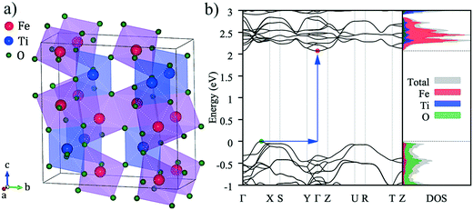
The calculated electronic band structure of pseudobrookite Fe2TiO5 is shown in Fig. 1b. The top of the valence band was set at 0 eV as the reference. The band diagram clearly illustrates that the pseudobrookite Fe2TiO5 is a semiconductor with an indirect band gap. The valence-band maximum (VBM) is located between the Γ point and the X point, while the conduction-band minimum (CBM) lies at the Γ point.The calculated indirect band gap of Fe2TiO5 was 2.07 eV, which is close to the experimental result for the bulk band gap: Eg = 2.1 eV.12 The optimized lattice parameters were a = 3.795 Å, b = 9.956 Å, c = 9.982 Å. The reported experimental lattice parameters are a = 3.732 Å, b = 9.793 Å, c = 9.979 Å,14 which indicates a deviation within 2% in our simulated crystal. The right-hand panel of Fig. 1b is the density of states (DOS). The dashed lines indicate the location of the VBM and the CBM. Although the valence band is composed mainly of O 2p electronic states, a significant contribution of Fe 3d (eg) character is also observed. The hybrid nature of the cation and anion bands is considered to be the origin of the strong dispersion of the VBM observed in Fig. 1b. The conduction band is composed of Fe 3d (t2g) states, and tails to lower energy than Ti, reducing the band gap energy of this system.
4.2. Experiment
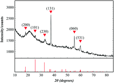
To check the crystallinity of the synthesized films, post-annealed films were investigated with X-ray diffraction. Fig. 2 shows the diffraction peaks of an Fe2TiO5 film that appear at 18.16°, 25.72°, 32.72°, 37.5°, 55.37° and 59.995°, corresponding to the (200), (101), (230), (131), (060) and (531) lattice directions of the pseudobrookite Fe2TiO5 structure (PDF#41-1432), respectively. No peaks of anatase TiO2 nor hematite Fe2O3 were observed, meaning that there is no phase separation. Although our fabrication method does not employ any epitaxial nor single crystal substrates, the film shows a continuous, closed and rather smooth morphology with preferential orientation. The XRD spectrum also indicated the preferential orientation of the film in the (131) direction. Such a structural nature is advantageous for many large-scale practical applications. Peak positions show a small deviation from the standard diffraction pattern due to the substantial difference in thermal expansion coefficients between Fe2TiO5 film and the substrates. Coefficients of thermal expansion of Fe2TiO5 on the a, b and c axes are 10.1 × 10⁻⁶, 16.3 × 10⁻⁶ and 0.6 × 10⁻⁶ (°C−1), which are highly anisotropic.27 Those values on the a and b axes are higher than that of Si (100) 2.6 × 10⁻⁶, and SiO2 (quartz) 5 × 10⁻⁷ (°C−1). Such a discrepancy generates a tensile stress in the film at the interface which in turn induces a peak shift as well as the preferential orientation in the film growth.Valence states and chemical composition at the surfaces of orthorhombic Fe2TiO5 films were studied with XPS analysis. High-resolution XPS spectra of Ti, Fe, and O are presented in Fig. 3. Ti 2p1/2 and Ti 2p3/2 peaks centered at 464.0 and 458.3 eV (Fig. 3a) evidently demonstrate that the Ti element exists principally in the Ti4+ state. In addition, two peaks at binding energies of 724.6 and 711.0 eV, accompanied by two satellites at 733.3 and 719.3 eV, were attributed to Fe 2p1/2 and Fe 2p3/2. This consistently indicated the Fe3+ oxidation state of the Fe element. The atomic percentage ratio of Ti![[thin space (1/6-em)]](https://www.rsc.org/images/entities/char_2009.gif) :
:![[thin space (1/6-em)]](https://www.rsc.org/images/entities/char_2009.gif) Fe obtained from the XPS data is 1.0
Fe obtained from the XPS data is 1.0![[thin space (1/6-em)]](https://www.rsc.org/images/entities/char_2009.gif) :
:![[thin space (1/6-em)]](https://www.rsc.org/images/entities/char_2009.gif) 2.0. This validated the near-ideal stoichiometry of our sputtered iron(III) titanate films. In the O 1s spectrum, there were two peaks of 530.0, 532.0 eV. The first O 1s peak could be accredited to O2− binding oxygen, coordinated with Fe and Ti. The second peak might arise from oxygen at the interface and/or contamination.
2.0. This validated the near-ideal stoichiometry of our sputtered iron(III) titanate films. In the O 1s spectrum, there were two peaks of 530.0, 532.0 eV. The first O 1s peak could be accredited to O2− binding oxygen, coordinated with Fe and Ti. The second peak might arise from oxygen at the interface and/or contamination.
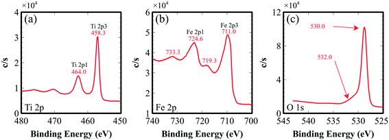 | ||
| Fig. 3 XPS spectra of the Fe2TiO5 thin film: (a) Ti 2p spectrum, (b) Fe 2p spectrum, (c) O 1s spectrum. The energies were calibrated with the C 1s peak at 285 eV. | ||
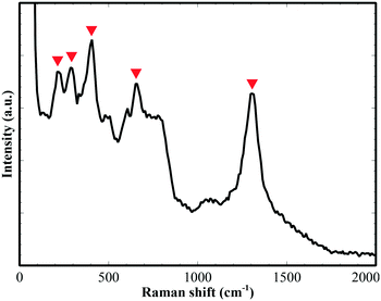
Fig. 4 shows a Raman spectrum of ex situ annealed Fe2TiO5 film, taken with an excitation wavelength of 532 nm. Several Raman characteristic peaks of Fe2TiO5 could apparently be observed at 217, 292, 394, 657 and 1294 cm−1. There were substantial peak shifts compared with previous work by Bersani et al.28 This could be due to the difference in Ti![[thin space (1/6-em)]](https://www.rsc.org/images/entities/char_2009.gif) :
:![[thin space (1/6-em)]](https://www.rsc.org/images/entities/char_2009.gif) Fe ratio and fabrication method. While in the former work,28 iron titanate films were synthesized with a sol–gel process and the maximum Ti
Fe ratio and fabrication method. While in the former work,28 iron titanate films were synthesized with a sol–gel process and the maximum Ti![[thin space (1/6-em)]](https://www.rsc.org/images/entities/char_2009.gif) :
:![[thin space (1/6-em)]](https://www.rsc.org/images/entities/char_2009.gif) Fe ratio reached only 1
Fe ratio reached only 1![[thin space (1/6-em)]](https://www.rsc.org/images/entities/char_2009.gif) :
:![[thin space (1/6-em)]](https://www.rsc.org/images/entities/char_2009.gif) 1.5; in the present case, RF sputtering deposition was utilized and a ratio of 1.0
1.5; in the present case, RF sputtering deposition was utilized and a ratio of 1.0![[thin space (1/6-em)]](https://www.rsc.org/images/entities/char_2009.gif) :
:![[thin space (1/6-em)]](https://www.rsc.org/images/entities/char_2009.gif) 2.0 could be obtained.
2.0 could be obtained.
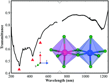
For further structural characterization, the FT-IR spectrum of sputtered iron titanate film on silicon substrate was taken from 200 to 1200 cm−1 (Fig. 5). The film crystal structure consisted mainly of six-fold coordinated Ti and Fe, illustrated as edge-sharing (TiO6) and (FeO6) octahedra. Two absorption peaks at around 432 and 290 cm−1 could be assigned to vertically aligned Ti–O stretching29 and horizontal plane O–Ti–O bending vibrations of (TiO6) octahedra. The last peak at 513 cm−1 could be assigned to some vibration in the (FeO6) octahedra. However, these assignments need further study for clarification.
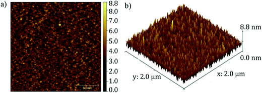
The morphology of Fe2TiO5 film was investigated with SEM and AFM (Fig. 6 and 7). The surface of the Fe2TiO5 films contained well-defined nearly-oriented nanoscale hills and valleys with an average roughness of approximately 4.4 nm. An SEM image of the film deposited with in situ annealing at the same temperature is also presented in Fig. 6 for further comparison. Different domains consisted of small crystallites orienting in certain directions. The signature of a preferential orientation as well as the nanofacets might indicate that interface energy partly motivates the flat and closed nature of the film. Prior works using dry synthesis have adopted co-deposition from TiO2 and Fe2O3 targets, but only the work done with pulsed laser deposition (PLD) has reported successful results.30 This would point to the necessity of very high temperature during the crystal growth or a highly excited state of the incoming flux. In the current synthesis, we used a stoichiometric Fe2TiO5 sputter target (from Furuuchi Kagaku: mostly sintered above 1100 °C from TiO2 and Fe2O3 particles) and obtained successful film growth. We grew the film only at 550 °C, but the target itself is already in the form of Fe2TiO5. This will be the major reason why we readily obtained high-quality films by sputter deposition.
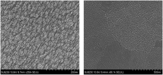 | ||
| Fig. 6 SEM images of RF sputtered Fe2TiO5 on silicon substrate. The surface was covered with Pt before imaging. Ex situ annealing (left) and in situ annealing (right). | ||
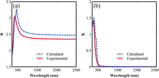
Ellipsometry was employed to characterize the refractive indices of Fe2TiO5 thin films with a Tauc–Lorentz model for fitting. The refractive index value (n) varies from 2.9 to 2.4 in the visible region (400–800 nm) (Fig. 8a). High extinction coefficient (k) values were observed below 500 nm and were reduced drastically above that, corresponding to the band gap energy of this system.
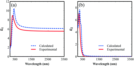
In order to compare and validate the accuracy of the calculations and experiments, we calculated the average dielectric functions (optical permittivity) and these are presented in Fig. 9. The real part of the calculated spectrum shape is in good agreement with the experimentally obtained optical permittivity in Fig. 9a. The imaginary part exhibits a peak around 400 nm related to the optical transitions between O 2p valence bands and Fe 3d conduction bands and tails to up to 600 nm, pointing to the good visible photoactivity of this material. We note here a noticeable difference between experimental and calculated optical spectra that could come from the experimental structures (grain and surface roughness), and/or the relatively simple independent-particle approximation model in our optical calculations.
Optical absorption of Fe2TiO5 thin film on glass was also studied with UV-vis spectroscopy (Fig. 10a). Fig. 10b displays the Tauc plot generated from the measured absorption spectrum, where α, h, and ν are the absorption coefficient, Planck constant, and photon energy, respectively. Direct and indirect band gap values were estimated to be 3.0 and 2.0 eV, by extrapolation of the curve.31,32 According to the DFT band calculation (Fig. 1b), the indirect and direct band gaps are mainly attributed to the excitation between O 2p states to Fe 3d state. The simulated Tauc plots calculated from absorption coefficients showed good agreement with experiment (Fig. 10c). The observed absorption properties strongly support the promising features for application in the photochemical and photoelectric conversion of the fabricated film in the visible region.
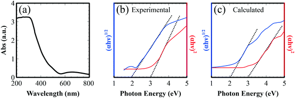 | ||
| Fig. 10 (a) UV-vis absorption spectrum of Fe2TiO5 thin film on glass; Tauc plot to extrapolate direct and indirect band gaps of (b) Fe2TiO5 films and (c) simulated results. | ||
5. Conclusion
We have reported for the first time the deposition of Fe2TiO5 thin films with RF magnetron sputtering on glass and silicon substrates. The as-deposited films were annealed in air ex situ at 550 °C for 2 hours to form a well-defined single phase. XRD exhibited a pseudobrookite structure oriented in the (131) direction. The average roughness measured for a 70 nm-thick film with AFM was about 4 nm. Direct and indirect band gap values extracted from Tauc plots were approximately 2.0 and 3.0 eV, respectively. DFT calculation also resulted in band gap values of 2.07 eV (indirect) and 3.0 eV (direct) from simulated Tauc plots, explaining the observed values. The good agreement of experimental and DFT simulated dielectric functions also helped to reveal the optical properties of Fe2TiO5 sputtered films. We hope that the synthesis method we propose here will pave the way for the large-scale production of Fe2TiO5 film for solar energy applications.Conflicts of interest
There are no conflicts of interest to declare.Acknowledgements
We thank Mr. Hirohito Ohata at Materials Analysis Station, National Institute for Materials Science (NIMS) for XPS analysis of Fe2TiO5 thin films; and Ms. Tomomi Sawada (MANA Foundry, NIMS) for her assistance in sputter deposition. The DFT calculations in this study were performed on Numerical Materials Simulator at NIMS. This work is partially supported by JSPS KAKENHI (16F16315, JP16H06364, 16H03820), and CREST “Phase Interface Science for Highly Efficient Energy Utilization” (JPMJCR13C3) from Japan Science and Technology Agency.References
- J. Deng, X. Lv, J. Liu, H. Zhang, K. Nie, C. Hong, J. Wang, X. Sun, J. Zhong and S.-T. Lee, ACS Nano, 2015, 9, 5348–5356 CrossRef CAS PubMed
.
- R. Li, Y. Jia, N. Bu, J. Wu and Q. Zhen, J. Alloys Compd., 2015, 643, 88–93 CrossRef CAS
.
- M. Dondi, F. Matteucci, G. Cruciani, G. Gasparotto and D. M. Tobaldi, Solid State Sci., 2007, 9, 362–369 CrossRef CAS
.
- P. Salarizadeh, M. Javanbakht, S. Pourmahdian, A. Bagheri, H. Beydaghi and M. Enhessari, J. Colloid Interface Sci., 2016, 472, 135–144 CrossRef CAS PubMed
.
-
NASA, Lunar Sample Mineralogy, https://curator.jsc.nasa.gov/lunar/letss/mineralogy.pdf
.
- S. Petit, S. T. A. G. Melissen, L. Duclaux, M. T. Sougrati, T. Le Bahers, P. Sautet, D. Dambournet, O. Borkiewicz, C. Laberty-Robert and O. Durupthy, J. Phys. Chem. C, 2016, 120, 24521–24532 CrossRef CAS
.
- H. Beydaghi, M. Javanbakht and E. Kowsari, Polymer, 2016, 87, 26–37 CrossRef CAS
.
- K.-M. Min, K.-S. Park, A.-H. Lim, J.-C. Kim and D.-W. Kim, Ceram. Int., 2012, 38, 6009–6013 CrossRef CAS
.
- S. Wang, N. Wu, Y. Liu, W. Liu and J. Liu, J. Alloys Compd., 2017, 714, 583–592 CrossRef CAS
.
- C.-L. Zhu, H.-L. Yu, Y. Zhang, T.-S. Wang, Q.-Y. Ouyang, L.-H. Qi, Y.-J. Chen and X.-Y. Xue, ACS Appl. Mater. Interfaces, 2012, 4, 665–671 CrossRef CAS
.
- S. Itoh, T. Suga, H. Takizawa and T. Nagasaka, ISIJ Int., 2007, 47, 1416–1421 CrossRef CAS
.
- H. Zhang, J. H. J. H. Kim, J. H. J. H. Kim, J. S. Lee, Z. Hemin, K. J. Hun, K. J. Hyun and L. J. Sung, Adv. Funct. Mater., 2017, 27, 1702428 CrossRef
.
- X. An, H. Lan, R. Liu, H. Liu and J. Qu, New J. Chem., 2017, 41, 7966–7971 RSC
.
- W. Q. Guo, S. Malus, D. H. Ryan and Z. Altounian, J. Phys.: Condens. Matter, 1999, 11, 6337–6346 CrossRef CAS
.
- Y. Yang, Y. Yu, J. Wang, W. Zheng and Y. Cao, CrystEngComm, 2017, 19, 1100–1105 RSC
.
- W. Lei, N. N. Truong and S. Patrik, ChemSusChem, 2016, 9, 2048–2053 CrossRef
.
- S. Sathasivam, D. S. Bhachu, Y. Lu, S. M. Bawaked, A. Y. Obaid, S. Al-Thabaiti, S. N. Basahel, C. J. Carmalt and I. P. Parkin, Chem. Vap. Deposition, 2015, 21, 21–25 CrossRef CAS
.
- G. Kresse and J. Furthmüller, Phys. Rev. B: Condens. Matter Mater. Phys., 1996, 54, 11169–11186 CrossRef CAS
.
- G. Kresse and J. Furthmüller, Comput. Mater. Sci., 1996, 6, 15–50 CrossRef CAS
.
- J. P. Perdew, K. Burke and M. Ernzerhof, Phys. Rev. Lett., 1996, 77, 3865–3868 CrossRef CAS
.
- J. D. Pack and H. J. Monkhorst, Phys. Rev. B: Solid State, 1977, 16, 1748–1749 CrossRef
.
- J. P. Perdew and A. Zunger, Phys. Rev. B: Condens. Matter Mater. Phys., 1981, 23, 5048–5079 CrossRef CAS
.
- V. I. Anisimov, J. Zaanen and O. K. Andersen, Phys. Rev. B: Condens. Matter Mater. Phys., 1991, 44, 943–954 CrossRef CAS
.
- A. Jain, S. P. Ong, G. Hautier, W. Chen, W. D. Richards, S. Dacek, S. Cholia, D. Gunter, D. Skinner, G. Ceder and K. A. Persson, APL Mater., 2013, 1, 011002 CrossRef
.
-
Materials Project, GGA+U calculations, https://materialsproject.org/wiki/index.php/GGA+U_calculations
.
- M. Gajdoš, K. Hummer, G. Kresse, J. Furthmüller and F. Bechstedt, Phys. Rev. B: Condens. Matter Mater. Phys., 2006, 73, 045112 CrossRef
.
- M. Zimmerman, D. Baskin, K. Faber, E. Fuller, A. Allen and D. Keane, Acta Mater., 2001, 49, 3231–3242 CrossRef CAS
.
- D. Bersani, P. P. Lottici and A. Montenero, J. Mater. Sci., 2000, 35, 4301–4305 CrossRef CAS
.
- P. Tarte, Nature, 1961, 191, 1002–1003 CrossRef CAS
.
- M. Osada, K. Nishio, H. Y. Hwang and Y. Hikita, APL Mater., 2018, 6, 056101 CrossRef
.
-
J. I. Pankove, Optical Processes in Semiconductors, Dover Publications, New York, 1975 Search PubMed
.
- J. Tauc, Mater. Res. Bull., 1968, 3, 37–46 CrossRef CAS
.
Footnote |
| † These authors contributed equally to this work. |
| This journal is © The Royal Society of Chemistry 2019 |


