 Open Access Article
Ink-jet patterning of graphene by cap assisted barrier-guided CVD†
Ding-Rui Chena,
Sheng-Kuei Chiub,
Meng-Ping Wua,
Chia-Chen Hsua,
Chu-Chi Tinga,
Mario Hofmann c and
Ya-Ping Hsieh
 *b
*b
aGraduate Institute of Opto-Mechatronics, National Chung Cheng University, Chiayi, 62102, Taiwan
bInstitute of Atomic and Molecular Sciences, Academia Sinica, Tainan 106, Taiwan. E-mail: yphsieh@gate.sinica.edu.tw
cDepartment of Physics, National Taiwan University, Tainan 106, Taiwan
First published on 17th September 2019
Abstract
Barrier-guided CVD growth could provide a new route to printed electronics by combining high quality 2D materials synthesis with scalable and cost-effective deposition methods. Unfortunately, we observe the limited stability of the barrier at growth conditions which results in its removal within minutes due to hydrogen etching. This work describes a route towards enhancing the stability of an ink-jet deposited barrier for high resolution patterning of high quality graphene. By modifying the etching kinetics under confinement, the barrier film could be stabilized and high resolution barriers could be retained even after 6 hours of graphene growth. Thus produced microscopic graphene devices exhibited an increase in conductivity by 6 orders of magnitude and a decrease in defectiveness by 48 times yielding performances that are superior to devices produced by traditional lithographical patterning which indicates the potential of our approach for future electronic applications.
Introduction
To date the development of electronic devices has been driven by their ever increasing performance and decreasing dimensions. However, for recently envisioned applications in wearable devices and distributed sensors, other metrics become more important. The cost of fabrication can be lowered by scalable methods such as screen printing, ink-jet deposition, and casting of liquid-based materials.1 Moreover liquid-based deposition approaches can enable device flexibility due to their compatibility with polymeric and biological substrates.While scalable deposition processes can produce complex circuits at a large scale, the resulting device performance is too low for many applications, necessitating large driving voltages2–4 or exhibiting slow response.5 The discovery of 2D materials could provide a route to alleviate these issues. Due to their atomic thickness 2D materials, such as MoS2 and graphene, are inherently transparent and flexible. Furthermore, they have shown high performance as conductors, sensors, and transistors that make them ideally suited as circuit elements.6–8 Advances in their scalable fabrication9 and economic transfer10 make it a serious competitor for future wearable and innovative devices11 if easy integration of 2D materials into complex circuits can be achieved.
Recently, the barrier-guided growth of graphene has shown the potential to provide a scalable route for patterning 2D materials without compromising their performance.12,13 In it, graphene is grown on a pre-patterned substrate that contains areas which are selectively passivated by a barrier material. The resulting graphene was shown to follow the shape of the exposed growth substrate and no graphene growth was observed within the barrier regions.
This method could increase the scalability of 2D material patterning since the concept is compatible with methods where the barrier is produced from liquid-deposited salts and oxides.14 Previous work has established that micrometer resolution patterns could thus be produced over large scale using ink-jet printing, stamping, or gravure printing.15–18 However, such processes are conducted at room temperature and no information exists about the fate of the barriers at the conditions required to grow graphene. Especially, the known instability of liquid-deposited inks at high temperatures19 puts the approach in question. Since 2D materials' growth will occur in any exposed catalyst region, even small cracks in the barrier will produce unwanted graphene features that could result in current leakage pathways in electronic devices. Moreover, many applications, such as heterojuction photosensors,20 require a high quality barrier as a functional element.
To address these issues, we here investigate routes towards improving the quality of printed barriers for high-resolution graphene patterning. We demonstrate that the currently achievable resolution is limited by the thermal stability of the printed barriers. Under graphene growth conditions an ink-jet deposited barrier was found to decompose quickly and disappear after 20 minutes of growth leaving behind un-patterned and defective graphene. Hydrogen etching was identified as the origin of this removal process. To overcome the limitation, we devised a method that modifies the kinetics of the etching process and favors the formation of a stable oxide. By employing an enclosure, stable and high resolution barriers could be formed even for long growth durations. The resulting patterned graphene exhibits high performance as confirmed by Raman spectroscopy and carrier transport characterization. The presented approach demonstrates a route to scalably produce microscopic patterns of graphene for future devices.
Experimental
Growth barriers were produced by ink-jet printing in a commercial ink-jet printer (Epson L220). As a precursor, aluminium chloride (Alfa Aesar) was dissolved in ethanol (0.16 g ml−1) and ultrasonicated.Copper foil (Alfa Aesar, 25 μm, 99.8%, Alfa-Aesar, no. 46365) served as the growth substrate. To remove imperfections from the copper foil, it was electrochemically polished in process phosphoric acid (85%) and then cleaned by rinsing with deionized water and blow drying by nitrogen.
To enhance the resolution of the printed patterns, the copper foil was first oxidized at 200 °C for 150 min. This process resulted in an increased contact angle (ESI Fig. 1†) and the resulting printed pattern transformed from individual dots into a continuous line (ESI Fig. 1†).
The pre-treated Cu foils were then used to carry out graphene growth following previous reports.21 First, the foils were annealed under hydrogen atmosphere for 70 min to initiate Cu grain growth and to remove organic residue and surface oxide. Graphene growth was conducted at 1030 °C under a gas mixture of H2 (200 sccm) and CH4 (10 sccm) for various time and rapidly cooled under 10 sccm hydrogen flow.
Results and discussion
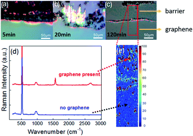
After graphene growth, the pre-patterned samples were characterized by optical microscopy and it was observed that even for short growth durations (5 min) holes occurred in the previously continuous barrier film (Fig. 1(b), compared to Fig. 1(a)). These holes increased in size and after 20 minutes only the edge regions and dispersed portions of the barrier remained (Fig. 1(c)).However, even for long growth durations (2 hours) some part of the barriers remained (Fig. 1(d)). Spatially resolved Raman spectroscopy indicates that at these conditions graphene grows throughout the sample including in regions that were covered by the barrier before (Fig. 1(f)). Surprisingly, the amount of graphene is similarly low in the previously covered and uncovered regions, indicating that residue from the barrier perturbs the graphene growth even at large distances from the barrier interface.
The observation that a barrier is quickly removed and negatively affects the growth throughout the sample puts the usefulness of the printing approach for barrier guided growth into question, especially in light of the long growth duration required for high quality graphene growth.22
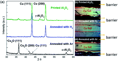
To identify the origin of the barrier instability at growth conditions, we modified the atmosphere inside the CVD reactor. It was observed that the presence of hydrogen limited the barrier stability. We found that the barriers would remain intact even after 6 hours of annealing when no hydrogen (only argon) was used (Fig. 2(d)). On the other hand, just 10 sccm of hydrogen flow would result in the removal of the barrier within minutes (Fig. 2(c)). This observation can be explained by the conversion of the barrier under growth conditions. X-ray diffraction indicates that the initially deposited barrier film contains γ-Al2O3 (Fig. 2(a)). This phase exhibits a defective fcc-structure and can easily be reduced by hydrogen at elevated temperatures and thus removed during graphene growth.23
In the absence of hydrogen no graphene growth was observed which could be due to the presence of surface oxides and a restructuring of the copper as observed by XRD (Fig. 2(a)).
The connection of graphene growth and barrier etching represents a critical challenge to barrier-guided growth and from liquid deposited barriers under realistic growth conditions. Therefore, a route of conversion from γ-Al2O3 into a more stable phase has to be devised that does not generate surface oxides as hydrogen-free annealing does.
We here introduce a new approach to transform the barrier oxide in a hydrogen environment. It relies on a method to selectively limit the etching process while the phase transformation occurs. If the etching process is slowed down sufficiently, a stable barrier phase will be generated before the barrier is etched.
We have previously demonstrated that the kinetics of CVD processes can be adjusted by controlling the precursor transport through spatial confinement which results in a molecular flow condition.24 We employ a cap on top of the barrier-passivated copper foil (Fig. 3(a)) that is expected to have three distinct functions; (1) decreasing or limiting the H2 gas flow to slow down the γ-Al2O3 etching process, (2) thus providing enough time for γ-Al2O3 to convert into the stable α-Al2O3 during the annealing period, and (3) providing optimized growth conditions for the synthesis of high quality graphene25
 | ||
| Fig. 3 (a) Schematic of the employed confinement approach where a graphite spacer is inserted between a quartz cap and copper. (b) Micrograph of patterned barrier before and after annealing. | ||
Our hypothesis is confirmed by the observation that capped barrier-guided graphene growth retains a distinct barrier even after 6 hour growth duration (Fig. 3(b)). The pronounced difference in morphology compared to uncapped annealing (Fig. 2(c)) demonstrates that the conversion process can be controlled by slowing down the hydrogen transport through the introduction of confinement and highlights the potential of our method.
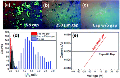
Moreover, it is found that adjusting the confinement conditions can produce different graphene morphologies far away from the barrier. While unconfined growth results in defective graphene (Fig. 4(a)), a gap size of 250 μm produces films of discontinuous graphene flakes (Fig. 4(b)). Finally, direct contact between growth substrate and cap yields continuous films (Fig. 4(c)).
To quantify the quality of thus produced graphene, we carry out Raman spectroscopy and find that the defect-related ID/IG ratio decreases from an average of 1.2 to 0.025 under identical growth conditions, by adjustment of the gap size (Fig. 4(d)). This change can be correlated with a decrease in graphene defectiveness from 3 × 1011 cm−2 to 6 × 109 cm−2.26 This significant lowering of the spatial density of defects in the grown graphene yields an enhancement in carrier conductivity by six orders of magnitude when an enclosure is used (Fig. 4(e)).
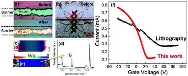
In addition to the improvements in the graphene conductivity, the pattern fidelity is significantly enhanced for our approach. Using an enclosure, the shape of the barrier could be retained with micrometer resolution as demonstrated when comparing the barrier morphology before and after growth of graphene (Fig. 5(a)). The changes before and after growth were found to be within 5 μm and the resolution is therefore only limited by the employed printing deposition. This high resolution and stability of barrier patterns after growing graphene is illustrated in Fig. 5(b) showing the same pattern before and after printing.
The use of an enclosure has the additional benefit of increased graphene quality under such conditions.21 We find that the produced graphene is of comparable quality to graphene grown without a barrier as demonstrated by Raman spectroscopy (Fig. 5(d)). On top of that, Raman Id/Ig mapping (Fig. 5(c)) shows clear boundaries along Al2O3 edges indicating an effective suppression of Al2O3 diffusion by cap enclosure during growth of graphene.
The ability to pattern graphene at high quality was employed to produce field effect transistors (Fig. 5(b)). The resulting transconductance characteristics are similar to the behavior of lithographically patterned FETs (Fig. 5(e)) but shows higher mobility (∼6000 cm2 V−1 s−1) as evidenced by a steeper slope and higher achievable current densities which could be attributed to the lithography-free fabrication of ink-jet patterning method.
Conclusions
In conclusion, we have demonstrated that enhanced thermal stability is required to produce microscopic graphene patterns by growth from ink-jet deposited barriers. Under conventional conditions, growth barriers are found to be removed within minutes, leaving behind an un-patterned and defective graphene film. This removal was found to originate from hydrogen etching at the growth conditions. By slowing down the hydrogen transport through use of an enclosure, this process could be limited and the resolution of barriers could be retained even after 6 hour growth. The resulting graphene exhibited high quality and could be patterned with high fidelity over large areas. Our results open a route for the scalable production of 2D materials for future electronic devices.Conflicts of interest
There are no conflicts to declare.Acknowledgements
Y.-P. Hsieh and M. Hofmann acknowledges financial support from Applied Materials, Inc., the Ministry of Science and Technology (Grant number 102-2112-M-194-003-MY3; 103-2218-E-006-004), and Industrial Technology Research Institute of Taiwan.References
- H. Bi, K. Yin, X. Xie, Y. Zhou, N. Wan, F. Xu, F. Banhart, L. Sun and R. S. Ruoff, Adv. Mater., 2012, 24, 5124–5129 CrossRef CAS PubMed.
- E. Sowade, E. Ramon, K. Y. Mitra, C. Martínez-Domingo, M. Pedró, J. Pallarès, F. Loffredo, F. Villani, H. L. Gomes, L. Terés and R. R. Baumann, Sci. Rep., 2016, 6, 33490 CrossRef CAS PubMed.
- P. Beecher, P. Servati, A. Rozhin, A. Colli, V. Scardaci, S. Pisana, T. Hasan, A. J. Flewitt, J. Robertson, G. W. Hsieh, F. M. Li, A. Nathan, A. C. Ferrari and W. I. Milne, J. Appl. Phys., 2007, 102, 043710 CrossRef.
- S. Chung, S. O. Kim, S. K. Kwon, C. Lee and Y. Hong, IEEE Electron Device Lett., 2011, 32, 1134–1136 CAS.
- S. Lilliu, M. Böberl, M. Sramek, S. F. Tedde, J. E. Macdonald and O. Hayden, Thin Solid Films, 2011, 520, 610–615 CrossRef CAS.
- B. Cho, M. G. Hahm, M. Choi, J. Yoon, A. R. Kim, Y.-J. Lee, S.-G. Park, J.-D. Kwon, C. S. Kim, M. Song, Y. Jeong, K.-S. Nam, S. Lee, T. J. Yoo, C. G. Kang, B. H. Lee, H. C. Ko, P. M. Ajayan and D.-H. Kim, Sci. Rep., 2015, 5, 8052 CrossRef CAS PubMed.
- S. Das, H.-Y. Chen, A. V. Penumatcha and J. Appenzeller, Nano Lett., 2013, 13, 100–105 CrossRef CAS PubMed.
- B. Liu, L. Chen, G. Liu, A. N. Abbas, M. Fathi and C. Zhou, ACS Nano, 2014, 8, 5304–5314 CrossRef CAS PubMed.
- Y.-P. Hsieh, C.-H. Shih, Y.-J. Chiu and M. Hofmann, Chem. Mater., 2016, 28, 40–43 CrossRef CAS.
- L. Gao, W. Ren, H. Xu, L. Jin, Z. Wang, T. Ma, L.-P. Ma, Z. Zhang, Q. Fu, L.-M. Peng, X. Bao and H.-M. Cheng, Nat. Commun., 2012, 3, 699 CrossRef PubMed.
- K. S. Novoselov, V. I. Fal'ko, L. Colombo, P. R. Gellert, M. G. Schwab and K. Kim, Nature, 2012, 490, 192 CrossRef CAS PubMed.
- M. Wang, L. Fu, L. Gan, C. Zhang, M. Rümmeli, A. Bachmatiuk, K. Huang, Y. Fang and Z. Liu, Sci. Rep., 2013, 3, 1238 CrossRef PubMed.
- N. S. Safron, M. Kim, P. Gopalan and M. S. Arnold, Adv. Mater., 2012, 24, 1041–1045 CrossRef CAS PubMed.
- M. Hofmann, Y.-P. Hsieh, A. L. Hsu and J. Kong, Nanoscale, 2014, 6, 289–292 RSC.
- P. M. Grubb, H. Subbaraman, S. Park, D. Akinwande and R. T. Chen, Sci. Rep., 2017, 7, 1202 CrossRef PubMed.
- J. Li, S. Sollami Delekta, P. Zhang, S. Yang, M. R. Lohe, X. Zhuang, X. Feng and M. Östling, ACS Nano, 2017, 11, 8249–8256 CrossRef CAS PubMed.
- E. B. Secor, S. Lim, H. Zhang, C. D. Frisbie, L. F. Francis and M. C. Hersam, Adv. Mater., 2014, 26, 4533–4538 CrossRef CAS PubMed.
- C. H. Chen, K. M. Reddy and N. P. Padture, Nanotechnology, 2012, 23, 6 Search PubMed.
- B. J. Perelaer, A. W. M. de Laat, C. E. Hendriks and U. S. Schubert, J. Mater. Chem., 2008, 18, 3209–3215 RSC.
- Y.-P. Hsieh, C.-H. Yen, P.-S. Lin, S.-W. Ma, C.-C. Ting, C.-I. Wu and M. Hofmann, Appl. Phys. Lett., 2014, 104, 041110 CrossRef.
- Y.-P. Hsieh, Y.-J. Chiu and M. Hofmann, Nanoscale, 2015, 7, 19403–19407 RSC.
- H. Zhou, W. J. Yu, L. Liu, R. Cheng, Y. Chen, X. Huang, Y. Liu, Y. Wang, Y. Huang and X. Duan, Nat. Commun., 2013, 4, 2096 CrossRef PubMed.
- M. Hartman, O. Trnka and O. Šolcová, Ind. Eng. Chem. Res., 2005, 44, 6591–6598 CrossRef CAS.
- H. T. Chin, C. H. Shih, Y. P. Hsieh, C. C. Ting, J. N. Aoh and M. Hofmann, Phys. Chem. Chem. Phys., 2017, 19, 23357–23361 RSC.
- H.-T. Chin, J.-J. Lee, M. Hofmann and Y.-P. Hsieh, Sci. Rep., 2018, 8, 4046 CrossRef PubMed.
- L. G. Cançado, A. Jorio, E. H. M. Ferreira, F. Stavale, C. A. Achete, R. B. Capaz, M. V. O. Moutinho, A. Lombardo, T. S. Kulmala and A. C. Ferrari, Nano Lett., 2011, 11, 3190–3196 CrossRef PubMed.
Footnote |
| † Electronic supplementary information (ESI) available: Microscope images and complete Raman spectra. See DOI: 10.1039/c9ra03117k |
| This journal is © The Royal Society of Chemistry 2019 |


