 Open Access Article
A zwitterionic polymer as an interfacial layer for efficient and stable perovskite solar cells†
Suyuan
Zhou‡
a,
Tao
Zhu‡
a,
Luyao
Zheng
a,
Dong
Zhang
c,
Wenzhan
Xu
a,
Lei
Liu
a,
Gang
Cheng
 *b,
Jie
Zheng
 *c and
Xiong
Gong
 *a
*a
aDepartment of Polymer Engineering, The University of Akron, Akron, OH 44325, USA. E-mail: xgong@uakron.edu
bDepartment of Chemical Engineering, University of Illinois at Chicago, Chicago, IL 60607, USA. E-mail: gangcheng@uic.edu
cDepartment of Chemical and Biomedical Engineering, The University of Akron, Akron, OH 44325, USA. E-mail: zhengj@uakron.edu
First published on 25th September 2019
Abstract
Perovskite solar cells have been rapidly developed in the past ten years. It was demonstrated that the interfacial layer plays an important role in device performance of perovskite solar cells. In this study, we report utilization of a photoinitiation-crosslinked zwitterionic polymer, namely dextran with carboxybetaine modified by methacrylate (Dex-CB-MA), as an interfacial layer to improve the film morphology of the CH3NH3PbI3 photoactive layer and the interfacial contact between the poly(3,4-ethylenedioxythiophene)-poly(styrenesulfonate) (PEDOT:PSS) hole extraction layer and CH3NH3PbI3 photoactive layer. It is found that the Dex-CB-MA thin layer forms a better band alignment between the PEDOT:PSS hole extraction layer and CH3NH3PbI3 photoactive layer, and improves the crystallization of the CH3NH3PbI3 photoactive layer, resulting in efficient charge carrier transport. As a result, perovskite solar cells with the PEDOT:PSS/Dex-CB-MA hole extraction layer exhibit more than 30% enhancement in efficiency and dramatically boosted stability as compared with that with the PEDOT:PSS hole extraction layer. Our studies provide an effective and facile way to fabricate stable perovskite solar cells with high power conversion efficiency.
1. Introduction
Perovskite solar cells (PSCs) have attracted great attention in both the academic and industrial sectors as the next-generation photovoltaic technology.1–5 Power conversion efficiencies (PCEs) have been rapidly boosted from 3.8% to over 23.7% in the past 10 years.6 Currently, PSCs incorporating a mesoporous TiO2 electron extraction layer (EEL) and PSCs with a planar heterojunction (PHJ) device structure are under investigation.7–9 As compared with the PSCs incorporating the TiO2 EEL, PHJ PSCs are more promising for practical applications due to their advanced potentials for high-throughput manufacturing processibility.10–13 However, poor device performance, in particular, low PCEs of PHJ PSCs restricted its practice applications.14 To circumvent these issues, the interfacial engineering was applied to improve device performance of PHJ PSCs.15–17 In general, the interfacial layers, which are used to reengineer the interfaces between perovskite photoactive layer and the EEL or the hole extraction layer (HEL), play an important role in device performance of PHJ PSCs.18,19 It has been demonstrated that the interfacial layers can tune the energy level at the perovskite/electrode interface, resulting in an ohmic contact from a Schottky barrier20,21 and improve charge transport, restricting charge carrier recombination as well.15,17 It was also reported that the interfacial layers can enhance the light-trapping, boosting light absorption in the photoactive layer22,23 and modulate the film morphology of photoactive layer, reducing surface defects and enhancing the stability of PHJ PSCs.24,25 Previously, we demonstrated that 4-lithium styrenesulfonic acid/styrene copolymer, and poly(2,2,6,6-tetra-methylpiperidinyloxy-4-yl-methacrylate)-co-(4-benzoylphenyl methacrylate) used as the interfacial layers can boost both PCEs and stability of PHJ PSCs.15,17In this study, we report the utilization a photoinitiation-crosslinked zwitterionic polymer, in particular, dextran with carboxybetaine modified by methacrylate (Dex-CB-MA), as an interfacial layer between the poly(3,4-ethylenedioxythiophene)-poly(styrenesulfonate) (PEDOT:PSS) hole extraction layer (HEL) and CH3NH3PbI3 photoactive layer. Systematically investigation indicates both the film morphology of CH3NH3PbI3 photoactive layer and the interfacial contact between the PEDOT:PSS HEL and CH3NH3PbI3 photoactive layer are tuned, resulting in the efficient charge transfer process, restricted surface charge carrier recombination. As a result, the PSCs with the PEDOT:PSS/Dex-CB-MA HEL exhibit a short-circuit current (JSC) of 19.90 mA cm−2, an open-circuit voltage (VOC) of 0.95 V, a fill factor (FF) of 74% and with a corresponding PCE of 13.81%, which is over 30% enhancement as compared with the PSCs with solely PEDOT:PSS HEL. Moreover, the PSCs with the PEDOT:PSS/Dex-CB-MA HEL exhibit dramatically enhanced stability.
2. Results and discussion
Fig. 1a presents the molecular structure of Dex-CB-MA, one of zwitterionic polymers with non-conjugate glucose unites as the backbone and functionalized with zwitterionic carboxyl betaine and double bond methacrylate group.26,27 Dex-CB-MA has negligible absorption in visible reign (ESI, Fig. S1†), but it can be photo-initiated to crosslink forming a robust thin-film.28–31Fig. 1b shows the transmittance spectra of the ITO/PEDOT:PSS and the ITO/PEDOT:PSS/Dex-CB-MA thin films. Both ITO/PEDOT:PSS and ITO/PEDOT:PSS/Dex-CB-MA thin films have a similar transmittance spectrum ranging from 350 nm to 800 nm, indicating that introduction of Dex-CB-MA thin layer on the top of PEDOT:PSS thin film will not tune the transmittance spectrum profile of ITO/PEDOT:PSS anode layer. Over 90% incident light passing through both ITO/PEDOT:PSS and ITO/PEDOT:PSS/Dex-CB-MA thin films would allow CH3NH3PbI3 photoactive layer to absorb large amounts of photons for generating decent photocurrent in PSCs.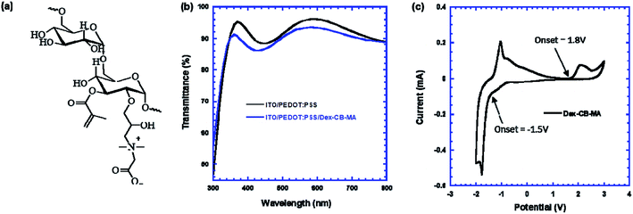 | ||
| Fig. 1 (a) The molecular structure of Dex-CB-MA, (b) the transmittance spectra of ITO/PEDOT:PSS and ITO/PEDOT:PSS/Dex-CB-MA thin films, (c) the cyclic voltammetry curve of Dex-CB-MA thin film. | ||
It was well-know that the highest occupied molecular orbit (HOMO) presents the energy required to extract an electron from a molecule, which is similar to an oxidation process, and the lowest unoccupied molecular orbit (LUMO) is the energy necessary to inject an electron to a molecule, which is a reduction process. Such processes, therefore, could be measured by cyclic voltammetry (CV) method from the oxidation and reduction potentials.32Fig. 1c presents the CV curve of Dex-CB-MA thin film. The oxidation and reduction potentials are estimated to be 1.8 V, and −1.5 V, respectively. Thus, the HOMO energy level and the LUMO energy level of Dex-CB-MA thin film are estimated to be −6.2 eV and −2.9 eV, respectively, according to the empirical equations E(HOMO) = −e[Eox(onset) + 4.4] and E(LUMO) = −e[Ered(onset) + 4.4].32
Fig. 2 presents the static contact angles of water on the surfaces of the PEDOT:PSS thin film and the PEDOT:PSS/Dex-CB-MA thin film, respectively. Compared with the contact angle (12.6°) observed from the PEDOT:PSS thin film, greatly enlarged contact angle (60.6°) observed from of the PEDOT:PSS/Dex-CB-MA thin film indicates that the Dex-CB-MA thin layer could decrease the surface tension of the PEDOT:PSS thin film, which is favorable for CH3NH3PbI3 to form large grain size with less grain boundaries,33 resulting in enhanced charge carrier mobility, consequently, boosted JSC from PSCs.34
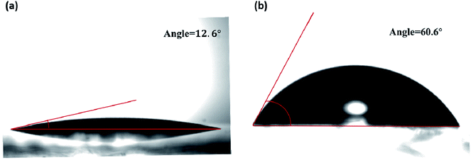 | ||
| Fig. 2 The contact angles of water on the thin films of (a) glass/PEDOT:PSS thin film and (b) glass/PEDOT:PSS/Dex-CB-MA thin film. | ||
Scheme 1a displays PSCs device structure of ITO/PEDOT:PSS/Dex-CB-MA/CH3NH3PbI3/PC61BM/Al, where PC61BM acts as the electron extraction layer and Al is aluminum, respectively. Scheme 1b presents the LUMO and HOMO energy levels of Dex-CB-MA, CH3NH3PbI3 and PC61BM, and the work functions of ITO, PEDOT:PSS and Al, respectively. It is clear that the LUMO energy level of Dex-CB-MA thin film is higher than that of CH3NH3PbI3 thin film, indicating that photo-generated electrons from CH3NH3PbI3 thin film can be efficiently blocked to contact with the ITO/PEDOT:PSS bilayer anode, suppressing surface charge carrier recombination. As a result, boosted JSC is expected to be observed from PSCs incorporated with the PEDOT:PSS/Dex-CB-MA HEL. However, the HOMO energy level of Dex-CB-MA thin film is much lower than the work function of PEDOT:PSS and the HOMO energy level of CH3NH3PbI3 thin film, so the thickness of the Dex-CB-MA layer should be tiny enough otherwise photo-generated holes from CH3NH3PbI3 thin film would be blocked and cannot be efficiently collected by the ITO/PEDOT:PSS bilayer anode. Towards the end, Dex-CB-MA with different thicknesses of 1 nm, 2 nm, and 5 nm, are investigated (Fig. S2 and Table S1 in ESI†).
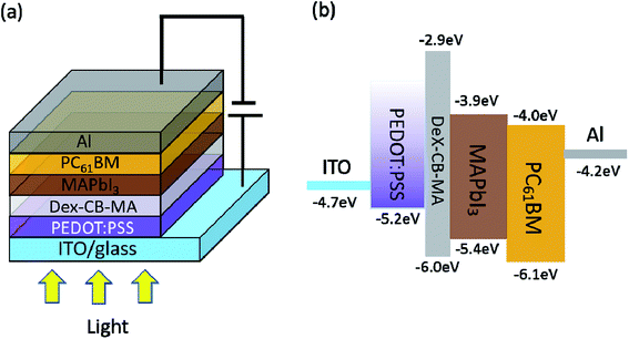 | ||
| Scheme 1 (a) The device structure of perovskite solar cells, and (b) the LUMO and HOMO energy levels of Dex-CB-MA, CH3NH3PbI3, PC61BM, and the work functions of ITO, PEDOT:PSS and Al. | ||
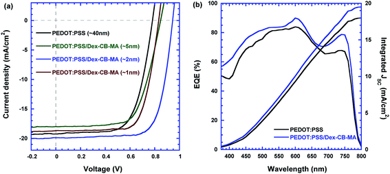
Fig. 3a presents the current density versus voltage (J–V) characteristics of PSCs incorporated with the Dex-CB-MA interfacial layers with different thickness under white light illumination with a light intensity of 100 mW cm−2. The device performance parameters are summarized in Table 1. The PSCs with ∼40 nm PEDOT:PSS HEL exhibit a JSC of 19.25 mA cm−2, a VOC of 0.80 V, a FF of 68%, and with a corresponding PCE of 10.42%. These device performance parameters are consistent with results reported previously.35,36 The PSCs incorporated with the PEDOT:PSS (∼40 nm)/Dex-CB-MA (∼1 nm) HEL show a JSC of 18.70 mA cm−2, a VOC of 0.82 V, an FF of 72%, and with a corresponding PCE of 11.17%. The PSCs incorporated with the PEDOT:PSS (∼40 nm)/Dex-CB-MA (∼2 nm) HEL exhibit a JSC of 19.90 mA cm−2, a VOC of 0.95 V, an FF of 74%, and with a corresponding PCE of 13.81%, which is about over 30% enhancement as compared with that of the PSCs only incorporated with solely PEDOT:PSS EEL. However, the PSCs incorporated with the PEDOT:PSS (∼40 nm)/Dex-CB-MA (∼5 nm) HEL show a JSC of 17.98 mA cm−2, a VOC of 0.85 V, an FF of 66%, and with a corresponding PCE of 10.11%. Such poor device performance is attributed to the thicker Dex-CB-MA interfacial layer due to its poor electrical conductivity.
| Hole extraction layers | J SC (mA cm−2) | V OC (V) | Fill factor (%) | PCE (%) |
|---|---|---|---|---|
| a The average parameters were calculated from 18 devices. | ||||
| PEDOT:PSS | 18.11[±0.3] (19.25) | 0.78[±0.3] (0.80) | 66.2[±0.2] (68.0) | 9.35[±1.03] (10.42) |
| PEDOT:PSS/Dex (∼5 nm) | 17.13[±0.7] (17.98) | 0.83[±0.3] (0.85) | 64.1[±0.2] (66.0) | 9.11[±0.96] (10.11) |
| PEDOT:PSS/Dex (∼2 nm) | 19.21[±0.3] (19.90) | 0.92[±0.2] (0.95) | 71.3[±0.3] (74.1) | 12.61[±1.09] (13.81) |
| PEDOT:PSS/Dex (∼1 nm) | 18.26[±0.6] (18.70) | 0.82[±0.1] (0.82) | 70.9[±0.8] (72.1) | 10.61[±0.42] (11.17) |
Fig. 3b demonstrates the EQE spectra of PSCs based on the PEDOT:PSS HEL and the PEDOT:PSS/Dex-CB-MA (2 nm) HEL. It is observed that two curves have similar profiles while EQE of the PSCs with the PEDOT:PSS/Dex-CB-MA (2 nm) HEL is increased, which is consistent with larger JSC obtained from the PSCs with PEDOT:PSS/Dex-CB-MA (2 nm) HEL. The integrated JSC, which is calculated by integration of EQE spectra are 18.27 mA cm−2 and 19.85 mA cm−2 for PSCs with the PEDOT:PSS HEL and the PEDOT:PSS/Dex-CB-MA (2 nm) HEL, respectively. These values are consistent with those from J–V characteristics.
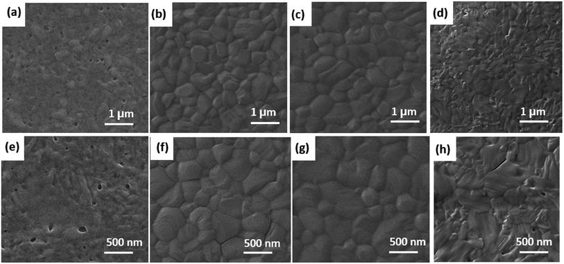
To study the influence of Dex-CB-MA interfacial layer on the film morphology and crystallinity of CH3NH3PbI3 photoactive layer, film morphologies of CH3NH3PbI3 coated on the top of the PEDOT:PSS EEL and the PEDOT:PSS/Dex-CB-MA HEL are investigated. The SEM images of CH3NH3PbI3 thin layers on the top of the PEDOT:PSS HEL and PEDOT:PSS/Dex-CB-MA HEL, where the thicknesses of Dex-CB-MA are 1 nm, 2 nm, and 5 nm are shown in Fig. 4. The film morphologies of CH3NH3PbI3 layers were improved by employing the Dex-CB-MA interfacial layers on the top of PEDOT:PSS layer. It is obvious that pinholes were dramatically reduced from the CH3NH3PbI3 thin film on the top of the PEDOT:PSS/Dex-CB-MA (2 nm) layer. Moreover, the largest crystal size with the fewest grain boundaries was also observed from the CH3NH3PbI3 thin film on the top of the PEDOT:PSS/Dex-CB-MA (2 nm) layer. All these would result in enhanced JSC and FF for PSCs. Therefore, as expected, the PSCs based on the PEDOT:PSS/Dex-CB-MA (2 nm) HEL possess superior device performance. In contrast, pinholes were easily observed on the surface of CH3NH3PbI3 thin film on the top of PEDOT:PSS thin layer. With a rough surface of CH3NH3PbI3 thin film on the top of the PEDOT:PSS/Dex-CB-MA (1 nm) HEL, pinholes and defects are still existed, which would result in poor JSC. The surface was optimized by the increased thickness of Dex-CB-MA, while the 5 nm Dex-CB-MA layer decreased the electrical conductivity of PEDOT:PSS/Dex-CB-MA (5 nm) HEL. As a result, JSC was reduced. Thus, the PSCs based on the PEDOT:PSS/Dex-CB-MA (5 nm) HEL exhibit poor PCE.
To further understand the underlying device performance of PSCs incorporated with the PEDOT:PSS/Dex-CB-MA HEL, surface charge recombination is investigated. Fig. 5a presents the light intensity dependence of JSC of the PSCs based on the PEDOT:PSS HEL and the PSCs based on the PEDOT:PSS/Dex-CB-MA HEL. According to the power-law fitting of JSC ∝ Iα, where I is the intensity of light, and α is the coefficient,36 the PSCs based on the PEDOT:PSS HEL have an α of 0.92, while the PSCs based on the PEDOT:PSS/Dex-CB-MA HEL have an α of 0.95. The closer to 1α is, the weaker of non-geminated recombination is in PSCs, which indicates that more charge carriers are extracted before they recombine with opposite charges. Fig. 5b shows the light intensity dependence of VOC of PSCs. With the formula of VOC ∝ S![[thin space (1/6-em)]](https://www.rsc.org/images/entities/char_2009.gif) ln(I), the VOC of control groups was more dependent on the light intensity.37 The VOC of the PSCs based on the PEDOT:PSS HEL had a slope of S = 2.79kBT/q, where kB is the Boltzmann constant, q is the elementary charge and T is the room temperature in Kelvin, while the VOC of the PSCs based on the PEDOT:PSS/Dex-CB-MA HEL had a slope of S = 1.31kBT/q. A smaller S means the less of trap-assisted charge recombination happening in PSCs.11 A less possibility of charge carrier recombination process indicates there are less traps acting as the center of recombination in perovskite thin films and more charge carriers are swept out to the electrodes. Those reduced charge carrier recombination process resulting from introducing Dex-CB-MA layer is also in agreement of enhanced JSC and VOC.
ln(I), the VOC of control groups was more dependent on the light intensity.37 The VOC of the PSCs based on the PEDOT:PSS HEL had a slope of S = 2.79kBT/q, where kB is the Boltzmann constant, q is the elementary charge and T is the room temperature in Kelvin, while the VOC of the PSCs based on the PEDOT:PSS/Dex-CB-MA HEL had a slope of S = 1.31kBT/q. A smaller S means the less of trap-assisted charge recombination happening in PSCs.11 A less possibility of charge carrier recombination process indicates there are less traps acting as the center of recombination in perovskite thin films and more charge carriers are swept out to the electrodes. Those reduced charge carrier recombination process resulting from introducing Dex-CB-MA layer is also in agreement of enhanced JSC and VOC.
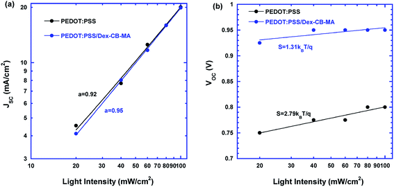 | ||
| Fig. 5 Light intensity dependence of (a) JSC and (b) VOC of perovskite solar cells with the PEDOT:PSS HEL and the PEDOT:PSS/Dex-CB-MA HEL. | ||
The J–V characteristics of PSCs in dark were measured to further verify and understand enhanced VOC for the PSCs based on the PEDOT:PSS/Dex-CB-MA HEL. As demonstrated in Fig. 6, when applied a reverse bias of −2 V, the dark current density of the PSCs based on the PEDOT:PSS HEL is about 10 times larger than that of the PSCs based on the PEDOT:PSS/Dex-CB-MA HEL. According to the formula of  ,38,39 where J0 is the reverse saturated dark current density, q is the elementary charge, n is diode ideality factor, T is the room temperature in Kelvin and kB is the Boltzmann's constant, the smaller the value of dark current density is, the higher VOC can be achieved in devices. The large difference between their dark currents indicates that by introducing the Dex-CB-MA thin layer, the trap states in CH3NH3PbI3 layer are suppressed, which is the reason that the PSCs based on the PEDOT:PSS/Dex-CB-MA (2 nm) HEL exhibit higher JSC and VOC.17
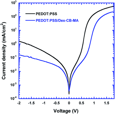 | ||
| Fig. 6 The J–V characteristics of perovskite solar cells with the PEDOT:PSS HEL and the PEDOT:PSS/Dex-CB-MA HEL, measured in dark. | ||
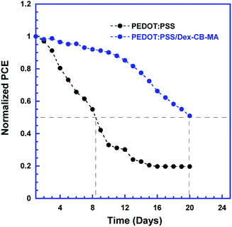
The stabilities of PSCs with different HELs were tested. Fig. 7 presents the self-stabilities of the PSCs with the PEDOT:PSS HELs and the PEDOT:PSS/Dex-CB-MA HEL, where un-encapsulated PSCs were stored in the glove box with a nitrogen atmosphere (O2 ∼ 100 ppm, H2O ∼ 0.1 ppm). It is clear that the PSCs with PEDOT:PSS/Dex-CB-MA HEL still maintains over 95% value of its original PCE after about one week while the PSCs with the PEDOT:PSS HEL remains only ∼60% value of its original PCE. After 20 days, PCE of the PSCs with the PEDOT:PSS/Dex-CB-MA HEL drops to 50% value of its initial and the PSCs with the PEDOT:PSS HEL left only ∼20% of its initial. For the PSCs based on the PEDOT:PSS HEL, the rapid decay in PCE at the beginning results from the deterioration in the interfacial layer, however, this process happened much later for the PSCs with the PEDOT:PSS/Dex-CB-MA HEL. These results indicate that the cross-linkable Dex-CB-MA formed a robust film to prevent the degradation of perovskite material because of the oxygen and moisture. It is obvious that the introduction of Dex-CB-MA interfacial layer can efficiently enhance the stability of PSCs, which is important for the commercial application of PSCs.
3. Conclusion
An ultrathin film of photoinitiation-crosslinked zwitterionic polymer, Dex-CB-MA, was used as an interfacial layer to improve both the film morphology of perovskite photoactive layer and the interfacial contact between the PEDOT:PSS hole extraction layer (HEL) and perovskite photoactive layer. It was found that the Dex-CB-MA interfacial layer can induce efficient charge transfer process in perovskite solar cells. As a result, the perovskite solar cells with the PEDOT:PSS/Dex-CB-MA HEL exhibited over 30% enhancement in power conversion efficiency as compared with the PSCs based the PEDOT:PSS HEL. In addition, the PSCs with the PEDOT:PSS/Dex-CB-MA HEL exhibited drastically enhanced stability. Thus, the utilization of Dex-CB-MA, a kind of transparent cross-linked polymer as an interfacial layer to reengineer the interfacial section in the solution-processed perovskite photoactive layer provides an effective and facile way to fabricate stable perovskite solar cells with high power conversion efficiency and good stability.4. Experimental section
4.1. Materials
N,N-dimethylglycine ethyl ester (98%) was purchased from TGI. Lead iodide (PbI2, 99.9985% metals basis) was purchased from Alfa Aesar. PEDOT:PSS (SCA 388-20) was purchased from Heraeus. Phenyl-C61-butyric acid methyl ester (PC61BM, 99.5%) was purchased from Solenne BV. Toluene (anhydrous, 99.8%), dimethylformamide (DMF, anhydrous, 99.8%), ethanol (anhydrous, >99.5%), dextran (10 kDa), sodium hydroxide (pelleted, >97%) and chlorobenzene (anhydrous, 99.8%) were purchased from Sigma-Aldrich. All materials are used as received without further treatment. Methylammonium iodide (MAI, CH3NH3I) was synthesized through hydroiodic acid and methylamine in our laboratory.40 Dex-CB-MA was prepared based on the method developed in our lab.41,424.2. PEDOT:PSS/Dex-CB-MA thin films
The ITO (indium tin oxides)/glass substrates were pre-cleaned by detergent, acetone, and isopropanol. Before casting any thin film on the top of ITO/glass substrates, the surface of ITO/glass substrates was treated by UV/Ozone for 20 minutes (min) at ambient atmosphere. After that, ∼ 40 nm thin layer of PEDOT:PSS was spin-coated on the top of ITO/glass substrates with a spin speed of 3500 rpm for 30 seconds (s), followed with thermal annealing at 150 °C on the hotplate for 10 min. The Dex-CB-MA thin films with different thicknesses were deposited on the top of PEDOT:PSS cast on the ITO/glass substrates from Dex-CB-MA (0.5 mg mL−1) mixed with 1% 2-hydroxy-4′-(2-hydroxyethoxy)-2-methyl propiophenone (as an initiator) with different spin-speed ranged from 1500 rpm to 3500 rpm. After that, the Dex-CB-MA thin films were immediately transferred to a glovebox with a nitrogen atmosphere, followed with UV light (365 nm) exposure for 2 hours at room temperature to photo-crosslink the Dex-CB-MA thin films.The transmittance spectra of both PEDOT:PSS thin layer and PEDOT:PSS/Dex-CB-MA thin layer were measured on HP 8453 spectrophotometer in ambient condition. The thicknesses of thin films were measured on a DektakXT surface profile system and further confirmed by atomic force microscopy (AFM) on Park System XE8. The top view images of scanning electron microscopy (SEM) of thin films were obtained on Tescan LYRA-3. The top images are by the SEM HV: 30.0 kV, SEM MAG: 50.0k× and the view field: 4.15 μm. The bottom images are by the SEM HV: 30.0 kV, SEM MAG: 100.0k× and the view field: 2.08 μm. Cyclic voltammetry spectrum of Dex-CB-MA thin film was obtained via the Gamry 600 plus to measure the oxidation and reduction potentials of Dex-CB-MA. Pt wire was used as the counter electrode. The Ag/AgCl electrode was used as the reference electrode while 0.1 M lithium perchlorate in acetonitrile used as the electrolyte. The contact angles of water on both PEDOT:PSS and PEDOT:PSS/Dex-CB-MA thin layers were measured on Angle Analysis Equipment from AST Products VCA Optima.
4.3. Fabrication and characterization of PSCs
The CH3NH3PbI3 photoactive layer was prepared by a two-step deposition method.15 Either PEDOT:PSS or PEDOT:PSS/Dex-CB-MA layers cast on the ITO/glass substrates were preheated at about 85 °C for 10 min. Warmed (∼85 °C) PbI2 DMF solution (400 mg mL−1) was then spin-coated on the top of either ITO/PEDOT:PSS or ITO/PEDOT:PSS/Dex-CB-MA layers at a spin rate of 6000 rpm for 20 s, followed with thermal annealing at 85 °C for 10 min. After PbI2 layer was cooled down to room-temperature, MAI layer was cast on the top of PbI2 layer from MAI ethanol solution (40 mg mL−1) at a spin rate of 6000 rpm for 35 s. After that, thin films were thermally annealed at 105 °C for 2 h on the hotplate for converting PbI2 and MAI into CH3NH3PbI3 thin film. After CH3NH3PbI3 thin film was cooled down to room temperature, a ∼40 nm PC61BM thin layer was spin-coated on the top of CH3NH3PbI3 thin film at 1500 rpm for 30 s from PC61BM chlorobenzene solution (20 mg mL−1). Afterwards, ∼100 nm aluminum (Al) electrode was thermally deposited on the top of PC61BM layer through a shadow mask with a base vacuum of 1 × 10⁻⁶ mbar. The active area of devices was measured to be ∼0.045 cm2.The current densities versus voltages (J–V) characteristics of PSCs were obtained by using a Keithley model 2400 source measure unit. A Newport Air Mass 1.5 Global (AM1.5 G) full-spectrum solar simulator was applied as the light source. The light intensity was 100 mW cm−2, which is calibrated by utilizing a mono silicon detector (with a KG-5 visible color filter) from the National Renewable Energy Laboratory to reduce the spectral mismatch. The external quantum efficiency (EQE) is obtained by using the solar cell quantum efficiency measurement system (QEX10) from PV measurements with a 300 W steady-state xenon lamp as the source light.
Conflicts of interest
There are no conflicts to declare.Acknowledgements
The authors acknowledge Air Force Scientific Research Program (FA9550-15-1-0292) and National Science Foundation (EECs 1351785 and EECs 1903303) for financial support.Notes and references
- R. Wang, M. Mujahid, Y. Duan, Z. K. Wang, J. Xue and Y. Yang, Adv. Funct. Mater., 2019, 1808843 CrossRef.
- J. Yan and B. R. Saunders, RSC Adv., 2014, 4, 43286–43314 RSC.
- W.-J. Yin, J.-H. Yang, J. Kang, Y. Yan and S.-H. Wei, J. Mater. Chem. A, 2015, 3, 8926–8942 RSC.
- J. Xiong, B. Yang, R. Wu, C. Cao, Y. Huang, C. Liu, Z. Hu, H. Huang, Y. Gao and J. Yang, Org. Electron., 2015, 24, 106–112 CrossRef CAS.
- C. Cao, C. Zhang, J. Yang, J. Sun, S. Pang, H. Wu, R. Wu, Y. Gao and C. Liu, Chem. Mater., 2016, 28, 2742–2749 CrossRef CAS.
- https://www.nrel.gov/pv/assets/pdfs/pv-efficiency-chart.20190103.pdf .
- Q. Hu, J. Wu, C. Jiang, T. Liu, X. Que, R. Zhu and Q. Gong, ACS Nano, 2014, 8, 10161–10167 CrossRef CAS.
- Y.-J. Jeon, S. Lee, R. Kang, J.-E. Kim, J.-S. Yeo, S.-H. Lee, S.-S. Kim, J.-M. Yun and D.-Y. Kim, Sci. Rep., 2014, 4, 6953 CrossRef CAS.
- J. Y. Jeng, Y. F. Chiang, M. H. Lee, S. R. Peng, T. F. Guo, P. Chen and T. C. Wen, Adv. Mater., 2013, 25, 3727–3732 CrossRef CAS.
- J. Sun, Y. Fu and Q. Wan, J. Phys. D: Appl. Phys., 2018, 51, 314004 CrossRef.
- C. Wang, C. Zhang, Y. Huang, S. Tong, H. Wu, J. Zhang, Y. Gao and J. Yang, Synth. Met., 2017, 227, 43–51 CrossRef CAS.
- Q. Chen, H. Zhou, Z. Hong, S. Luo, H.-S. Duan, H.-H. Wang, Y. Liu, G. Li and Y. Yang, J. Am. Chem. Soc., 2013, 136, 622–625 CrossRef.
- Y.-Q. Wang, S.-B. Xu, J.-G. Deng and L.-Z. Gao, R. Soc. Open Sci., 2017, 4, 170980 CrossRef.
- K. Wang, C. Liu, P. Du, J. Zheng and X. Gong, Energy Environ. Sci., 2015, 8, 1245–1255 RSC.
- L. Zheng, S. Mukherjee, K. Wang, M. E. Hay, B. W. Boudouris and X. Gong, J. Mater. Chem. A, 2017, 5, 23831–23839 RSC.
- G. Yang, C. Wang, H. Lei, X. Zheng, P. Qin, L. Xiong, X. Zhao, Y. Yan and G. Fang, J. Mater. Chem. A, 2017, 5, 1658–1666 RSC.
- K. Wang, C. Liu, C. Yi, L. Chen, J. Zhu, A. Weiss and X. R. Gong, Adv. Funct. Mater., 2015, 25, 6875–6884 CrossRef CAS.
- C.-C. Chueh, C.-Z. Li and A. K.-Y. Jen, Energy Environ. Sci., 2015, 8, 1160–1189 RSC.
- S. Feng, Y. Yang, M. Li, J. Wang, Z. Cheng, J. Li, G. Ji, G. Yin, F. Song and Z. Wang, ACS Appl. Mater. Interfaces, 2016, 8, 14503–14512 CrossRef CAS.
- K. M. O'Malley, Z. Li, L. C. Yip, Y. H. Jen and A. K. Adv, Energy Mater., 2012, 2, 82–86 CrossRef.
- C.-Z. Li, C.-C. Chueh, H.-L. Yip, K. M. O'Malley, W.-C. Chen and K.-Y. A. Jen, J. Mater. Chem., 2012, 22, 8574–8578 RSC.
- J. Y. Kim, S. H. Kim, H. Lee, K. Lee, W. Ma, X. Gong and A. J. Heeger, Adv. Mater., 2006, 18, 572–576 CrossRef CAS.
- A. K. K. Kyaw, D. H. Wang, D. Wynands, J. Zhang, T.-Q. Nguyen, G. C. Bazan and A. J. Heeger, Nano Lett., 2013, 13, 3796–3801 CrossRef CAS.
- B. Meng, Y. Fu, Z. Xie, J. Liu and L. Wang, Macromolecules, 2014, 47, 6246–6251 CrossRef CAS.
- Y. Shi, L. Tan, L. Chen and Y. Chen, J. Mater. Chem. C, 2014, 2, 8054–8064 RSC.
- H. Liu and J. Zhou, Prog. Chem., 2012, 11, 13 Search PubMed.
- Z. Zhang, S. Chen and S. Jiang, Biomacromolecules, 2006, 7, 3311–3315 CrossRef CAS.
- G. Mahmud, S. Huda, W. Yang, K. Kandere-Grzybowska, D. Pilans, S. Jiang and B. Grzybowski, Langmuir, 2011, 27, 10800–10804 CrossRef CAS.
- D. M. Guldi, C. Luo, N. A. Kotov, T. Da Ros, S. Bosi and M. Prato, J. Phys. Chem. B, 2003, 107, 7293–7298 CrossRef CAS.
- A. Sinclair, T. Bai, L. R. Carr, J.-R. Ella-Menye, L. Zhang and S. Jiang, Biomacromolecules, 2013, 14, 1587–1593 CrossRef CAS.
- L. Chen, X. Ouyang, A. Islam, M. Sain, J. Li, Z.-H. Lu and M. Pervaiz, Adv. Energy Mater., 2019, 1803354 Search PubMed.
- L. Leonat, G. Sbârcea and I. V. Brânzoi, UPB Sci. Bull. Ser. B Chem. Mater. Sci, 2013, 75, 111–118 CAS.
- M. B. Upama, N. K. Elumalai, M. A. Mahmud, D. Wang, F. Haque, V. R. Gonçales, J. J. Gooding, M. Wright, C. Xu and A. Uddin, Org. Electron., 2017, 50, 279–289 CrossRef CAS.
- C. Bi, Q. Wang, Y. Shao, Y. Yuan, Z. Xiao and J. Huang, Nat. Commun., 2015, 6, 1–7 Search PubMed; Q. Wang, Q. Dong, T. Li, A. Gruverman and J. Huang, Adv. Mater., 2016, 28, 6734–6739 CrossRef CAS.
- Y. Zheng, C. Wang, J. Yu, F. Yang, J. Zhang, B. Wei and W. Li, J. Phys. D: Appl. Phys., 2017, 50, 475303 CrossRef.
- N. K. McKinnon, D. C. Reeves and M. H. Akabas, J. Gen. Physiol., 2011, 138, 453–466 CrossRef CAS.
- Z. Li, W. Wang, N. C. Greenham and C. R. McNeill, Phys. Chem. Chem. Phys., 2014, 16, 25684–25693 RSC.
- W. Shockley and H. J. Queisser, J. Appl. Phys., 1961, 32, 510–519 CrossRef CAS.
- G. A. H. Wetzelaer, M. Kuik, M. Lenes and P. W. M. Blom, Appl. Phys. Lett., 2011, 99, 153506 CrossRef.
- X. Huang, K. Wang, C. Yi, T. Meng and X. Gong, Adv. Energy Mater., 2016, 6, 1–8 Search PubMed.
- B. Cao, L. Li, H. Wu, Q. Tang, B. Sun, H. Dong, J. Zhe and G. Cheng, Chem. Commun., 2014, 50, 3234–3237 RSC.
- W. N. E. van Dijk-Wolthuis, O. Franssen, H. Talsma, M. J. Van Steenbergen, J. J. Kettenes-Van Den Bosch and W. E. Hennink, Synthesis, Macromolecules, 1995, 28, 6317–6322 CrossRef CAS.
Footnotes |
| † Electronic supplementary information (ESI) available. See DOI: 10.1039/c9ra04907j |
| ‡ These authors are contributed to this work equally. |
| This journal is © The Royal Society of Chemistry 2019 |

