
 Open Access Article
 This Open Access Article is licensed under a Creative Commons Attribution-Non Commercial 3.0 Unported Licence
Planar graphitic ZnS, buckling ZnS monolayers and rolled-up nanotubes as nonlinear optical materials: first-principles simulation†
Lei Hu *a,
Wencai Yib,
Jianting Tanga,
Tongde Raoa,
Zuju Mac,
Chuanbo Hua,
Lei Zhanga and
Tingzhen Li*a
*a,
Wencai Yib,
Jianting Tanga,
Tongde Raoa,
Zuju Mac,
Chuanbo Hua,
Lei Zhanga and
Tingzhen Li*a
aSchool of Environmental and Chemical Engineering, Chongqing Three Gorges University, Chongqing, 404100, China. E-mail: huleisanxu@163.com; leihu@sanxiau.edu.cn; litingzhen@163.com
bSchool of Physics and Physical Engineering, Qufu Normal University, Qufu, 273165, China
cSchool of Materials Science and Engineering, Anhui University of Technology, Maanshan, 243002, China
First published on 15th August 2019
Abstract
Nonlinear optical (NLO) materials have an ability to generate new coherent light. At the present stage, three dimensional (3D) mid-infrared NLO materials suffer from various deficiencies such as low laser damage thresholds (LDTs) for AgGaQ2 (Q = S, Se); the band gaps of most intensively studied two-dimensional (2D) NLO materials are not wide enough to avoid two-photon absorption (TPA); a steady NLO property regardless of diameter and chirality is absent in one-dimensional (1D) single-walled nanotubes (SWNTs). In this research, the electronic and second harmonic generation (SHG) properties of planar graphitic ZnS (g-ZnS) monolayer, buckling reconstructed ZnS (R-ZnS) monolayer which is synthesized in a recent experiment, and rolled-up SWNTs are investigated with first-principles simulations. Theoretical results suggest the SHG coefficients of planar g-ZnS, buckling R-ZnS and rolled-up SWNTs are comparable with that of AgGaS2 crystals. The band gaps of planar g-ZnS and ZnS SWNTs are ∼3.8 eV, and that of buckling R-ZnS is as wide as ∼4.0 eV, indicating high LDTs and reduced TPA as NLO materials. The TPA edges can be further blue shifted by using incident light beams with a polarized electric field perpendicular to buckling R-ZnS. On the other hand, the TPA edges of ZnS SWNTs are nearly not affected by diameter and chirality. The SHG coefficients of ZnS SWNTs are much less influenced by chirality and diameter than those of SiC, GeC and BN SWNTs. Therefore, they are superior ultrathin NLO materials, and especially have a potential application in the mid-infrared regime where high-quality NLO crystals are emergently needed.
1. Introduction
Nonlinear optical (NLO) materials are very important because they have an ability to generate new coherent light with tunable frequencies that cannot be obtained directly from available lasers. At the present stage, typical NLO materials applied in the ultraviolet to near-infrared regimes have been well developed.1 However, the applications of commercial mid-infrared NLO materials AgGaQ2 (Q = S, Se) and ZnGeP2 are hindered by inherent defects, e.g. low laser damage thresholds (LDTs) for AgGaQ2, harmful two-photon absorption (TPA) for ZnGeP2, and a non-phase matching behavior in AgGaSe2.2 Therefore, high-quality NLO crystals which have potential applications in the mid-infrared regime are urgently needed.Recently, NLO phenomena in two-dimensional (2D) materials3,4 and one-dimensional (1D) single-walled nanotubes (SWNTs) with atomic thickness5–8 have become experimental and theoretical hotspots. 2D materials9 and 1D SWNTs5 usually display multiple van Hove singularities in the top of valence bands, which is the origin of large NLO susceptibilities.8 The atomic thickness of 2D materials and 1D SWNTs is much smaller than their coherent wavelength, so they will not suffer from the crucial phase-matching problem.10 Compared with bulk materials, atomic-thick materials exhibit wider band gaps because of the quantum size effect, e.g. 1.88 eV for monolayer MoS2 (ref. 11) versus 1.29 eV for bulk MoS2.12 However, the most intensively studied low-dimensional NLO material, i.e. monolayer MoS2 suffers from a significant deficiency in that the SHG coefficient in various experiments differs hugely, e.g. 5000 pm V−1 (ref. 13) vs. 320 pm V−1.14 This deficiency may be caused by strong TPA,15 which originates from lack of wide enough band gaps. Therefore, it is necessary to find low-dimensional NLO materials with stable SHG signals insensitive to TPA.
High LDTs also strongly depend on bandgaps. For typical mid-infrared materials with good NLO performance, the bandgaps should be preferably wider than 3.5 eV to satisfy academic and commercial purposes.1 Nevertheless, the bandgaps of experimentally discovered 2D NLO materials single-layer MoS2 (1.88 eV),11 MoSe2 (1.53 eV),16 InSe (2.14 eV)17,18 are relatively narrow. Even though it is still unknown the exact bandgap value of low dimensional NLO materials which is enough for academic and commercial purposes, it is no doubt that wide bandgaps enhance LDTs. Moreover, wide band gaps usually reduce optical transition possibilities which in turn result in small NLO coefficients. Therefore, search for atomic thick materials with wider bandgaps and large NLO coefficients becomes emergent.
On the other hand, bulk ZnS crystals find a variety of applications,19,20 e.g. NLO materials,20 light-emitting diodes21 and luminescence.22 Compared with bulk forms, 2D planar graphitic ZnS (g-ZnS) monolayer with zinc and sulfur atoms in the same plane is rarely investigated.23–28 Planar g-ZnS monolayer sustains large tensile and compressive strain,25 and especially under compressive strain planar g-ZnS is reconstructed into a buckling monolayer26 where zinc and sulfur atoms stay in various planes. To facilitate discussions, buckling reconstructed ZnS monolayer is denoted as R-ZnS in the following. The top and side views of buckling R-ZnS are given Fig. 1(a). The top view of planar g-ZnS is identical to that of buckling R-ZnS. In 2017, one atomic layer of ZnS (1 1 1) plane with buckling behaviors was successfully grown on Au (1 1 1).29 Notably, planar g-ZnS and buckling R-ZnS have direct band gaps, and their bandgaps are roughly estimated to be 4.21 and 4.70 eV respectively,27 which indicates high LDTs and reduced TPA as NLO materials. Therefore, in this research we explore the NLO properties of planar g-ZnS and buckling R-ZnS. As for ZnS SWNTs, previous studies merely focus on their structural, electronic, sensing and linear optical properties.30–34 Uniquely, the bandgaps of ZnS SWNTs are nearly chirality independent and weakly diameter dependent,34 indicating it is not necessary to exactly control the chirality and diameter to obtain one-dimensional SWNTs with the same band gap. Such a bandgap characteristic of ZnS SWNTs inspires to search for an steady NLO property regardless of chirality and diameter, which is absent in SiC,7 GeC8 and BN6 SWNTs.
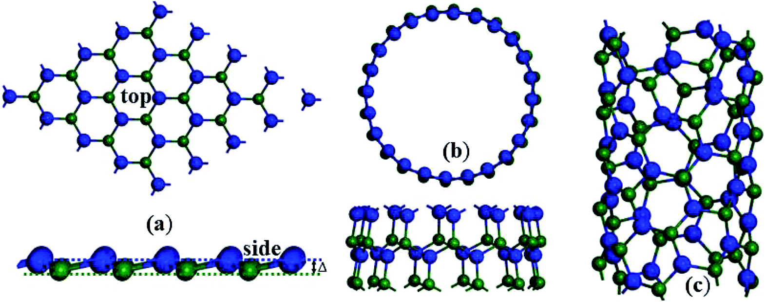 | ||
| Fig. 1 Top and side views of (a) buckling R-ZnS monolayer, (b) ZnS zigzag (12, 0) SWNT, and (c) schematic of ZnS chiral (6, 3) SWNT. The blue and green balls denote zinc and sulfur atoms respectively. | ||
Theoretical results demonstrate planar g-ZnS, buckling R-ZnS monolayers and rolled-up SWNTs exhibit large SHG coefficients comparable with that of typical AgGaS2, much wider band gaps than most ultrathin NLO materials, and no TPA in a wide optical energy range. Therefore, they are superior ultrathin NLO materials, and especially have a potential application in the mid-infrared regime where high-quality NLO materials are emergently needed. Moreover, the TPA edges of ZnS SWNTs are nearly regardless of chirality and diameter, and their SHG coefficients are much less influenced by chirality and diameter than other SWNTs. Finally, this work means a new family of ultrathin NLO materials, namely, group I–IV compounds MX (M = Zn, Cd; X = O, S, Se) related 2D and 1D materials.
2. Calculation methods
In the present work, the electronic and SHG properties of planar g-ZnS, buckling R-ZnS and rolled-up SWNTs are studied with first-principles calculations. All calculations are on the basis of density functional theory implemented in the VASP code.35–37 The generalized gradient approximation (GGA) is parametrized by PBE functional with van der Waals correction (DFT-D2).38,39 The plane-wave cutoff energy is set to 450 eV. To avoid interactions between adjacent monolayers or SWNTs, a large vacuum space of more than 10 Å is added. To overcome problems of bandgap underestimation caused by GGA-PBE, HSE06 hybrid functional with 25% Hartree–Fock exchange energy40 is utilized to calculate electronic band structures. As shown in Fig. S1 of ESI,† the band gap of wurtzite ZnS crystal calculated using HSE06 is 3.51 eV, which is very close to an experimental bandgap 3.77 eV.41 Furthermore, the energy difference between HSE06 and PBE bandgaps is applied for scissors corrections in SHG calculations.The formulism to calculate static and dynamic SHG coefficients is presented elsewhere,42 and has been successfully applied to predict the SHG coefficients of 2D InSe17 and bulk LiB3O3.43 Because a vacuum space of more than 10 Å is added, the effective unit-cell volume is in place of the unit cell volume when calculating optical properties. The effective unit-cell volume of planar g-ZnS and buckling R-ZnS is obtained by multiplying the in-plane area of unit cell and the effective thickness. Similar to planar g-SiC,7 the effective thickness d of planar g-ZnS is considered as the interlayer distance of optimized wurtzite ZnS [cf. Fig. S1 of ESI†]. The effective unit-cell volume of ZnS SWNTs is given by the equation V* = πDdT, where D and T are the diameter and the length of translational vectors for ZnS SWNTs respectively.
3. Results and discussions
3.1 Planar g-ZnS monolayer
For planar g-ZnS, the optimized in-plane lattice constant and Zn-S bond length are 3.876 and 2.238 Å respectively, which agree well with previously reported values.24 As shown in Fig. S2 of ESI,† planar g-ZnS displays a direct bandgap, with the valence band maximum (VBM) and conduction band minimum (CBM) both located at the Γ (0.0, 0.0, 0.0) point. The bandgaps obtained by PBE and HSE06 are 2.51 eV and 3.80 eV, respectively. HSE06 functional supplies reliable bandgaps which are comparable with experimental values. The HSE06 band gap of planar g-ZnS is apparently wider than that of intensively studied monolayer NLO materials MoS2 (1.88 eV),11 MoSe2 (1.53 eV)16 and InSe (2.14 eV).17 The wide bandgap of planar g-ZnS promises high LDTs and reduced TPA as NLO materials.To obtain trustable NLO coefficients, a quite dense k-point grid of 81 × 81 × 1 is applied to sample the Brillion zone, and 48 energy bands are included to allow complete optical transitions. Planar g-ZnS has four nonvanishing SHG coefficients at the static limit, i.e. χ(2)yyy(0) = −χ(2)yxx(0) = −χ(2)xxy(0) = −χ(2)xyx(0) dictated by D3H symmetry. The theoretical χ(2)xxy(0) of planar g-ZnS is 37.4 pm V−1, which is larger than χ(2)zxy(0) (31.72 pm V−1) of typical AgGaS2.44 The real and imaginary parts of χ(2)xxy of planar g-ZnS are given in Fig. 2(a). The imaginary part keeps zero until 1.9 eV, which corresponds to the half of the direct band gap of planar g-ZnS. The real part remains constant at low energies up to 1.0 eV. From 1.0 to 1.9 eV, the real part increases gradually and at 1.90 eV arrives at a small peak. The SHG spectra have pronounced structures contributed from single- and double-frequency resonant terms. To analyze these contributions, it is helpful to compare the absolute values of SHG coefficient |χ(2)xxy| and the absorptive part of dielectric function. As can be seen, the peaks a and g are caused by two-photon resonances [cf.  ]. The peak h is due to both one- and two-photon resonances. The prominent structure around k comes from one-photon resonances [cf.
  ].
].
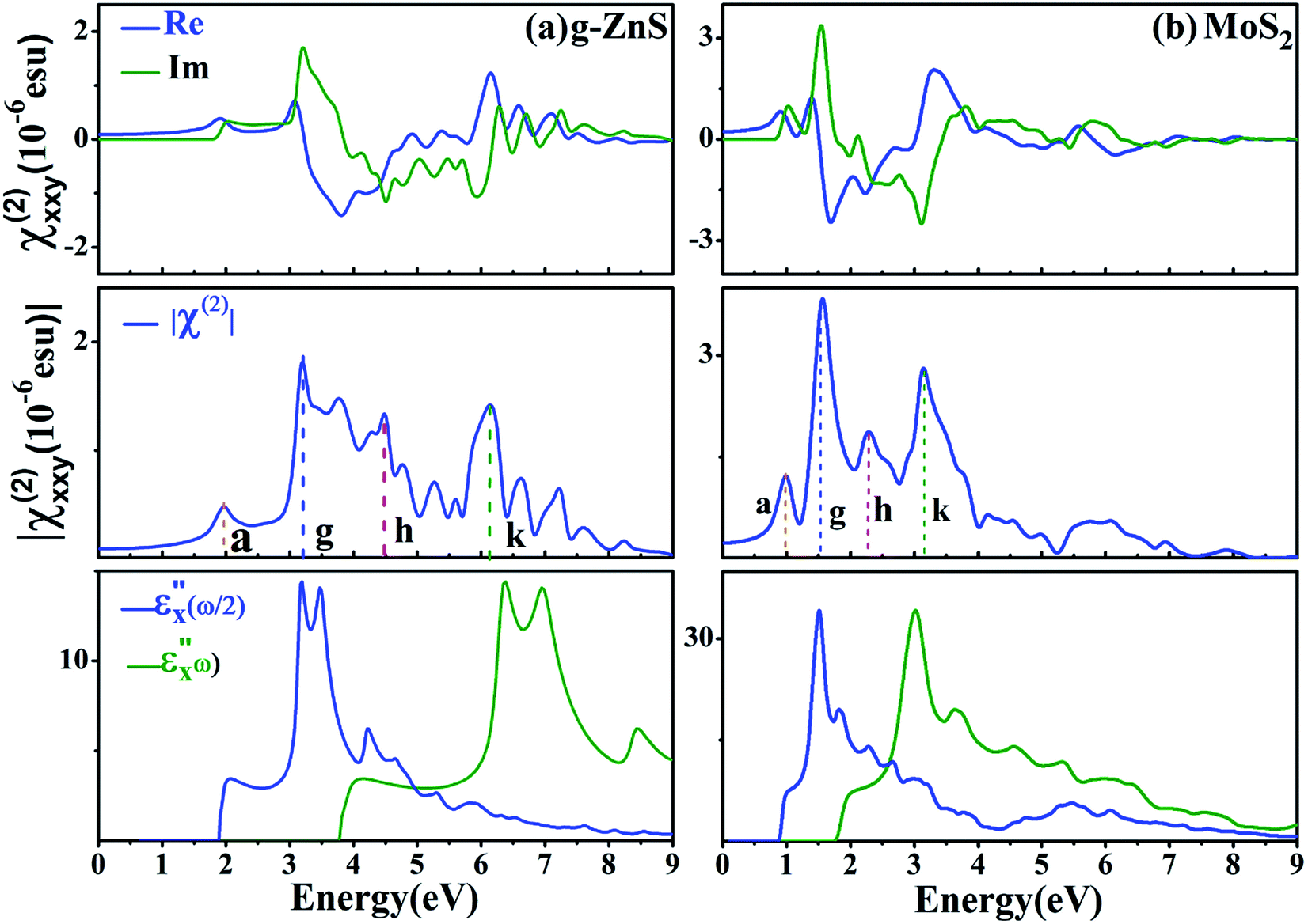 | ||
Fig. 2 Real (Re) and imaginary (Im) parts of SHG coefficient χ(2)xxy and absolute value of SHG coefficient |χ(2)xxy|, absorptive part of dielectric function  as a function of ω/2 and ω for (a) planar g-ZnS and (b) monolayer MoS2. as a function of ω/2 and ω for (a) planar g-ZnS and (b) monolayer MoS2. | ||
To further specify the potential application of planar g-ZnS in NLO devices, we compare the SHG property of planar g-ZnS with that of the intensively studied monolayer MoS2 in a previous theoretical calculation.45 Comparisons of Fig. 2(a) and (b) demonstrate that planar g-ZnS has two significant advantages over single-layer MoS2 as NLO materials. First, the absorption edge of χ(2)xxy for planar g-ZnS is located at 1.90 eV, while in sharp contrast, that of monolayer MoS2 is redshifted to 0.94 eV.15,45 As mentioned in the introduction, monolayer MoS2 suffers from a huge deficiency that the |χ(2)xxy| magnitude at 1.53 eV (810 nm) in various experiments differs hugely, e.g. 5000 pm V−1 (ref. 13) vs. 320 pm V−1.14 This deficiency of monolayer MoS2 may be caused by the strong TPA around 1.53 eV,15 and TPA also hinders application ranges of ZnGeP2 crystals.46 It is expected the |χ(2)xxy| magnitude of planar g-ZnS will not suffer from such problems because planar g-ZnS has no TPA below 1.90 eV. Secondarily, the nonvanishing |χ(2)xxy| of planar g-ZnS spans a more wide energy range. Moreover, as shown in ESI,† the estimated nonresonant SHG intensity of planar g-ZnS is larger than that of single-layer MoS2 because the refractive indices of planar g-ZnS are much smaller. The nonresonant SHG regime from zero to 1.9 eV of planar g-ZnS covers the whole mid-infrared regime (2–8 μm), so planar g-ZnS has a potential application in the mid-infrared regime.
3.2 Buckling ZnS monolayer
As mentioned in the introduction, single-layer ZnS with buckling behaviors was successfully grown on Au (1 1 1) in 2017.29 Hence, we simulate the NLO properties of five buckling ZnS monolayers R1-ZnS, R2-ZnS, R3-ZnS, R4-ZnS and R5-ZnS, which respectively have an in-plane constant, compressed by 1%, 2%, 3%, 4%, and 5% in comparison with that of planar g-ZnS. As shown in Fig. 1(a), the buckling parameter Δ of R-ZnS, defined as the z-coordinate differences of zinc and sulfur atoms and summarized in Table 1, increases with compressive strain. The effective thickness of buckling R-ZnS monolayer is considered as the sum of the effective thickness of planar g-ZnS and the buckling parameter. The band structures of buckling R-ZnS are calculated with HSE06 and given in Fig. S3 of ESI.† Buckling R-ZnS monolayers display direct bandgaps, and their band gaps are as wide as ∼4.0 eV. Such wide bandgaps have been rarely discovered before in 2D NLO materials except monolayer BN with a bandgap 6.07 eV.47| Materials | a | Δ | EPBEg | EHSEg | χ(2)xxy(0) | χ(2)zxx(0) | χ(2)zzz(0) |
|---|---|---|---|---|---|---|---|
| R1-ZnS | 3.837 | 0.024 | 2.63 | 3.90 | 34.22 | −1.52 | −1.00 |
| R2-ZnS | 3.798 | 0.035 | 2.74 | 4.01 | 31.08 | −2.22 | −1.47 |
| R3-ZnS | 3.760 | 0.279 | 2.77 | 4.00 | 29.14 | −17.16 | −11.70 |
| R4-ZnS | 3.721 | 0.351 | 2.79 | 3.98 | 28.08 | −21.90 | −15.56 |
| R5-ZnS | 3.682 | 0.450 | 2.71 | 3.81 | 25.76 | −26.61 | −20.44 |
In SHG calculations, the k-point mesh and energy bands of buckling R-ZnS are set as that of planar g-ZnS. Apart from χ(2)yyy(0) = −χ(2)yxx(0) = −χ(2)xxy(0) = −χ(2)xyx(0), buckling R-ZnS has another two-independent SHG coefficients χ(2)zxx(0) = χ(2)xzx(0) = χ(2)xxz(0) = χ(2)zyy(0) = χ(2)yyz(0) = χ(2)yzy(0) and χ(2)zzz(0) dictated by C3V symmetry. The theoretical χ(2)xxy(0), χ(2)zxx(0) and χ(2)zzz(0) are summarized in Table 1. Similar to planar g-ZnS, the static χ(2)xxy(0) of buckling R-ZnS is comparable with χ(2)zxy(0) of AgGaS2. χ(2)zzz(0) and χ(2)zxx(0) increase rapidly with buckling parameter, and for R5-ZnS, χ(2)zzz(0) and χ(2)zxx(0) are comparable with χ(2)xxy(0).
To further reveal the NLO characteristic of buckling R-ZnS monolayer, the real and imaginary parts of SHG coefficients χ(2)xxy, χ(2)zxx and χ(2)zzz of slightly buckling R1-ZnS, moderately buckling R3-ZnS and strongly buckling R5-ZnS are given in Fig. 3. As can be seen, the magnitude and line shape of χ(2)xxy for buckling R1-ZnS, R3-ZnS and R5-ZnS are almost not modified in comparison with that of planar g-ZnS. χ(2)zxx and χ(2)zzz of R1-ZnS are nearly vanishing, while those of R3-ZnS and R5-ZnS are of considerable magnitude and more resonant than χ(2)xxy.
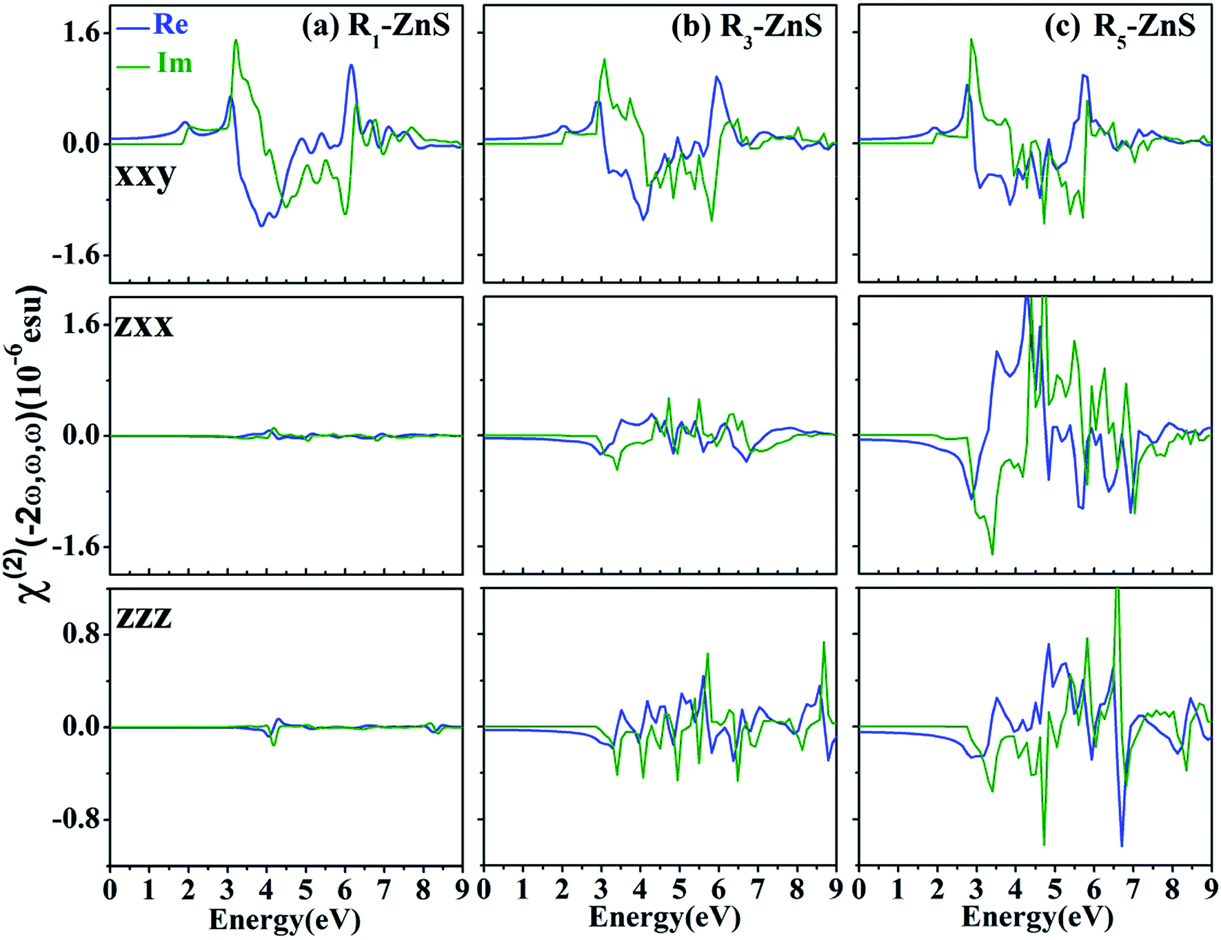 | ||
| Fig. 3 Real and imaginary parts of χ(2)xxy(−2ω, ω, ω), χ(2)zxx(−2ω, ω, ω) and χ(2)zzz(−2ω, ω, ω) of buckling R1-, R3-and R5ZnS monolayers. | ||
To analyze the contributions of single- and double-photon resonant terms to SHG spectra of buckling R-ZnS monolayer, we compare the absolute values of SHG coefficients |χ(2)xxy|, |χ(2)zzz| and |χ(2)zxx| of buckling R5-ZnS with the absorptive part of corresponding dielectric function in Fig. 4. As can be seen, similar to planar g-ZnS, the peaks a and g in the |χ(2)xxy| spectrum of buckling R5-ZnS are caused by two-photon resonances, the peak h in |χ(2)xxy| is due to both one- and two-photon resonances, and the peak k in |χ(2)xxy| comes from one-photon resonances. The peaks g and h in |χ(2)zzz| and |χ(2)zxx| are from double-photon resonances, while the peak k is due to both one- and double-photon resonances. More remarkably, the peak a in |χ(2)xxy| disappears in |χ(2)zzz|. Resultantly, the TPA edge of χ(2)zzz is blue-shifted even by ∼0.8 eV in comparison with that of χ(2)xxy, which is supported by the fact that the absorption edge of  is also blue shifted by ∼0.8 eV when compared with that of
  For χ(2)zzz, the polarized electric field of incoming and outgoing photons is perpendicular to buckling R-ZnS monolayer. Briefly, it is possible to further blue shift the TPA edges by using incident light beams with a polarized electric field perpendicular to buckling R-ZnS monolayer.
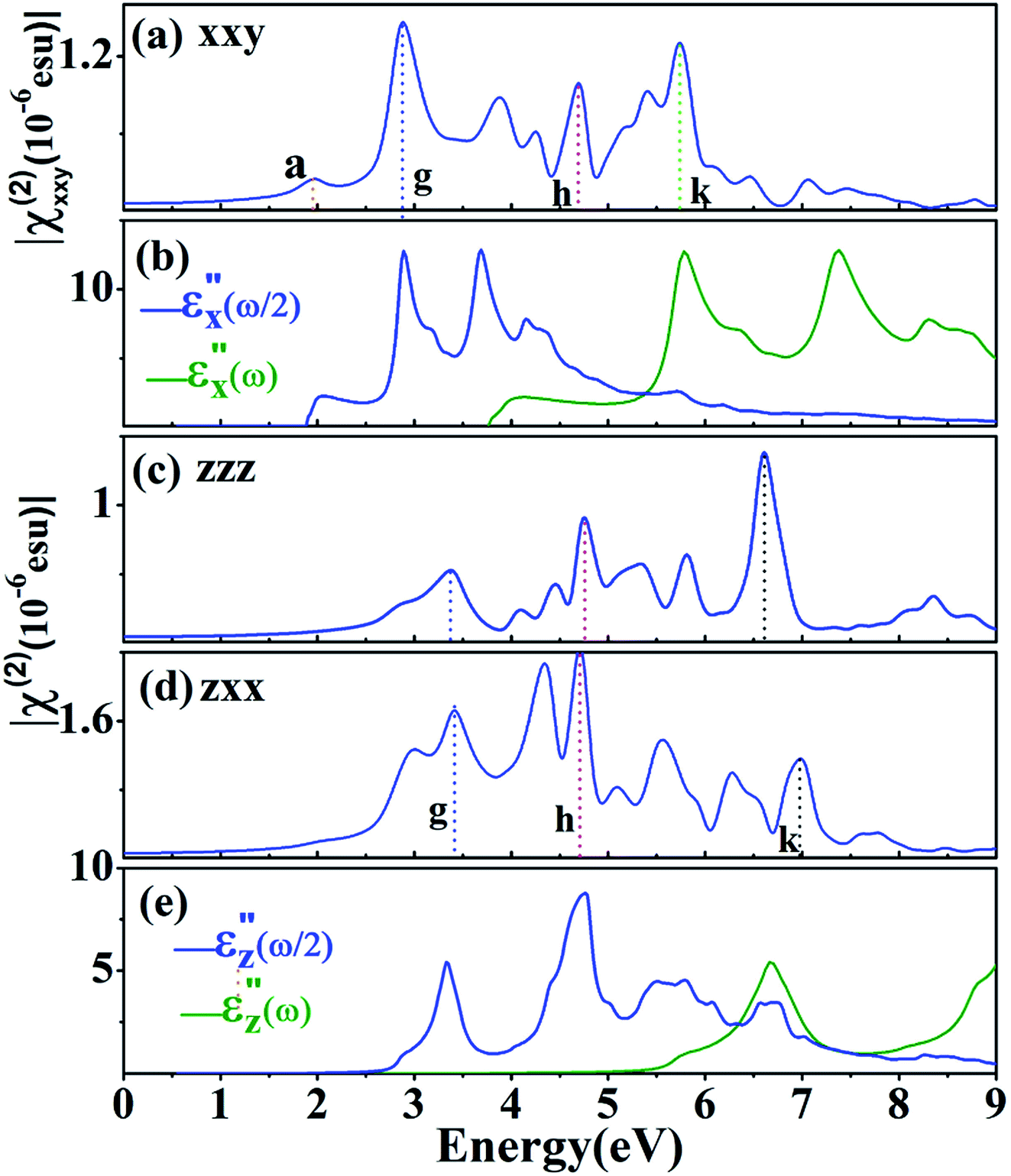 | ||
Fig. 4 Absolute value of SHG coefficients (a) |χ(2)xxy|, (c) |χ(2)zzz| and (d) |χ(2)zxx|, absorptive part of dielectric function (b)  and (e) and (e)  as a function of ω/2 and ω. as a function of ω/2 and ω. | ||
Moreover, Table S1 of ESI† suggests the refractive indices of buckling R-ZnS are nearly not modified when compared with that of planar g-ZnS. The small refractive indices of buckling R-ZnS will enhance the SHG intensity in the nonresonant regime which covers the mid-infrared regime.
3.3 Single-walled nanotubes
We have investigated the electronic and SHG properties of ZnS (6, 0), (8, 0), (9, 0), (10, 0), (12, 0), (16, 0), (18, 0), (20, 0) zigzag SWNTs, (4, 2) and (6, 3) chiral SWNTs. As shown in Fig. 1, the optimized zigzag and chiral SWNTs present buckling behaviors. Their theoretical diameters and lengths of translational vectors are summarized in Table 2. As suggested by Fig. S4 of ESI,† ZnS zigzag and chiral SWNTs display direct band gaps, with the VBM and CBM both located at the Γ (0.0, 0.0, 0.0) point. Meanwhile, a high density of states appears near the top of valence bands, which is helpful for optical interband transitions to occur near the Γ point. The HSE06 band gaps of all ZnS zigzag and chiral SWNTs are steady around 3.80 eV with a variance being ∼0.1 eV. By contrast, the bandgap variances of SiC SWNTs, GeC and BN SWNTs are as large as ∼0.70 eV,48 ∼2.4 eV (ref. 8) and ∼1.70 eV (ref. 49) respectively. The wide bandgaps of ZnS SWNTs are particularly important for NLO materials to enhance LDTs, but have not been discovered in NLO SiC7 and GeC8 SWNTs.| Species | D | T | EPBEg | EHSEg | χ(2)zxx(0) | χ(2)zzz(0) |
|---|---|---|---|---|---|---|
| (6, 0) | 7.55 | 6.43 | 2.71 | 3.77 | −14.40 | 50.14 |
| (8, 0) | 9.94 | 6.51 | 2.69 | 3.81 | −16.34 | 45.68 |
| (9, 0) | 11.11 | 6.54 | 2.71 | 3.85 | −16.86 | 43.20 |
| (12, 0) | 14.96 | 6.57 | 2.65 | 3.84 | −17.40 | 41.30 |
| (16, 0) | 19.82 | 6.61 | 2.64 | 3.87 | −17.56 | 39.20 |
| (18, 0) | 22.25 | 6.61 | 2.64 | 3.87 | −17.68 | 38.91 |
| (20, 0) | 24.74 | 6.63 | 2.62 | 3.86 | −17.60 | 38.76 |
| (4, 2) | 6.62 | 17.15 | 2.68 | 3.72 | −6.48 | 26.96 |
| (6, 3) | 9.78 | 17.31 | 2.68 | 3.78 | −8.84 | 24.26 |
In SHG calculations, the number of conduction bands is set as twice that of valence bands for all ZnS SWNTs, and a quite dense k-point mesh of 1 × 1 × m with m being 40 to 81 is applied to sample the Brillion zone of all SWNTs except (20, 0). The k-point grid of 1 × 1 × 31 is adopted for (20, 0), because as many as 1080 energy bands are essentially included. As dictated by Kleinman symmetry, ZnS zigzag and chiral SWNTs have two independent SHG coefficients in the static limit, i.e. χ(2)zzz(0) and χ(2)zxx(0) = χ(2)xxz(0) = χ(2)xzx(0) = χ(2)zyy(0) = χ(2)yyz(0) = χ(2)yzy(0). Their theoretical χ(2)zzz(0) and χ(2)zxx(0) are summarized in Table 2. The static χ(2)zzz(0) of ZnS zigzag SWNTs with small diameter such as (6, 0), (8, 0) and (9, 0) is larger than χ(2)xxy(0) of planar g-ZnS, while χ(2)zzz(0) of large-diameter (16, 0), (18, 0) and (20, 0) approaches χ(2)xxy(0) of planar g-ZnS. As the diameter increases, χ(2)zzz(0) for ZnS zigzag SWNTs decreases. The difference of χ(2)zzz(0) for small-diameter (6, 0) and large-diameter (20, 0) ZnS SWNTs is ∼12 pm V−1. By contrast, the variances of χ(2)zzz(0) between small- and large-diameter SiC, GeC, BN and ZnO zigzag SWNTs are as huge as ∼250 pm V−1,7 ∼150 pm V−1,8 ∼45 pm V−1,6 and ∼30 pm V−1 (ref. 50) respectively. In brief, the SHG coefficients of ZnS SWNTs are much less influenced by diameter. The χ(2)zzz(0) of ZnS (4, 2) and (6, 3) chiral SWNTs is comparable with χ(2)zxy(0) of AgGaS2, and not significantly modified in comparison with that of ZnS zigzag SWNTs.
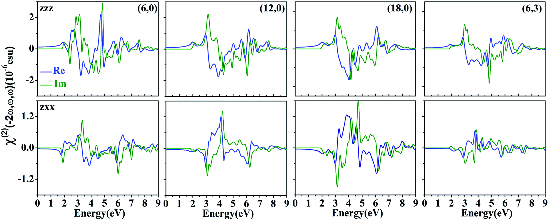
To further understand NLO characteristics of ZnS SWNTs, the real and imaginary parts of χ(2)zzz and χ(2)zxx of zigzag (6, 0), (12, 0), (18, 0) and chiral (6, 3) SWNTs are given in Fig. 5. The most pronounced character is that, the imaginary parts of χ(2)zzz and χ(2)zxx for the four SWNTs keep zero until ∼1.90 eV regardless of chirality and diameter. The variances in the real parts of both χ(2)zzz and χ(2)zxx are negligible from zero to 1.0 eV, so stable SHG signals can be achieved in a wide optical energy range from 0 to 1.0 eV. Therefore, it is not necessary to exactly control the chirality and diameter to obtain steady SHG signals relying upon ZnS SWNTs in a wide range of optical energies.
 | ||
| Fig. 5 Real and imaginary parts of χ(2)zzz and χ(2)zxx of ZnS zigzag (6, 0), (12, 0), (18, 0) and chiral (6, 3) SWNTs. | ||
As for the line shape, generally the spectra of each of χ(2)zzz and χ(2)zxx of the four SWNTs look similar. χ(2)zzz and χ(2)zxx of small-diameter (6, 0) SWNT are more resonant than that of (12, 0) and (18, 0) SWNTs. To analyze pronounced structures in the SHG spectra contributed from single- and double-frequency terms of ZnS SWNTs, the absolute values of χ(2)zzz and χ(2)zxx of a representative (12, 0) SWNT are plotted and compared with the absorption part of dielectric funiction  in Fig. 6. As can be seen, the main peaks a, g, h and k in the |χ(2)zzz| spectrum are well reproduced in |χ(2)zxx|. The peaks a and g in |χ(2)zzz| and |χ(2)zxx| are caused by two-photon resonances, the prominent structure h is due to both single- and double-photon resonances, and the peak k mainly comes from one-photon resonances. In brief, the direct band gap of (12, 0) as well as other ZnS SWNTs is around 3.80 eV, so they will exhibit no TPA below ∼1.90 eV. Moreover, Table S2 of ESI† suggests the refractive indices of ZnS SWNTs are nearly not modified in comparison with that of planar g-ZnS. The small refractive indices of ZnS SWNTs will enhance their SHG intensity in the nonresonant regime which covers the mid-infrared regime, so they have potential applications in the mid-infrared regime.
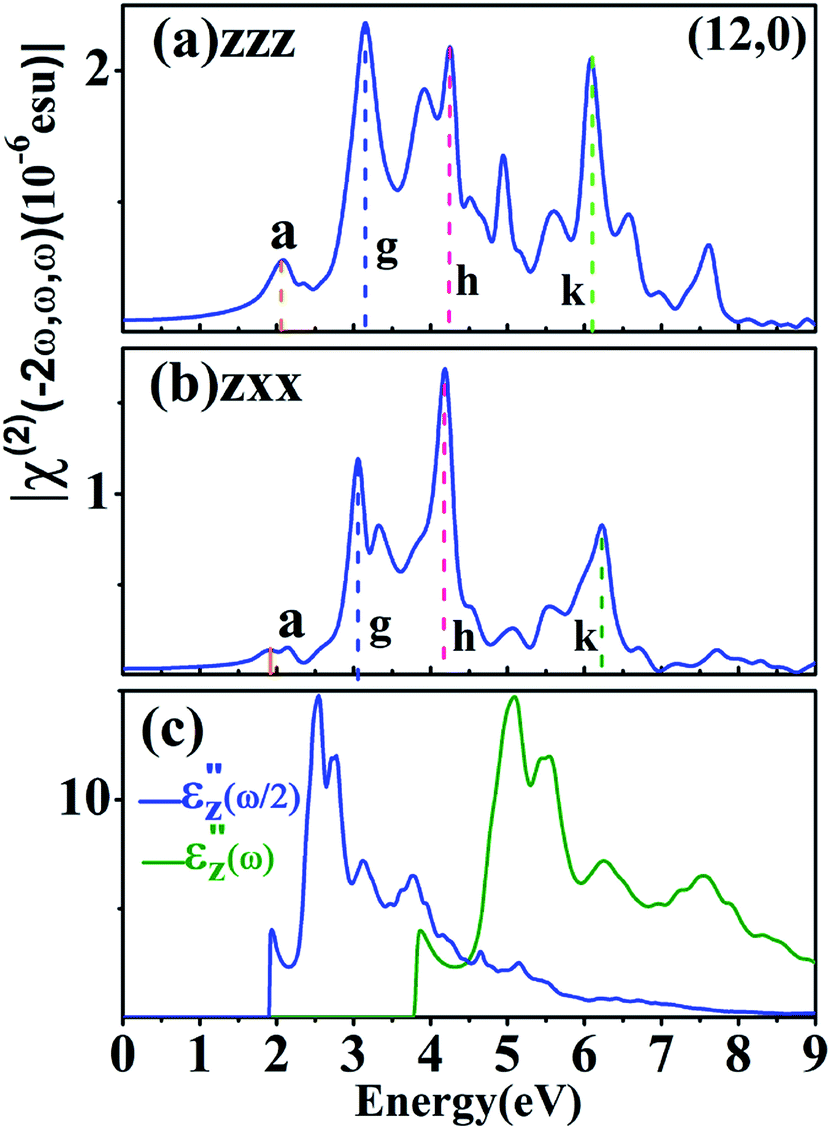 | ||
Fig. 6 Absolute value of the SHG coefficients (a) χ(2)zzz and (b) χ(2)zxx, and (c) absorptive part of dielectric function  as a function of ω/2 and ω of a representative (12, 0) SWNT. as a function of ω/2 and ω of a representative (12, 0) SWNT. | ||
4. Conclusions
We have performed first-principles simulations of electronic and SHG properties of planar g-ZnS, bucking ZnS monolayers and rolled-up SWNTs. Theoretical results reveal the SHG coefficients of planar g-ZnS, buckling R-ZnS and rolled-up SWNTs are comparable with that of typical AgGaS2. The band gaps of planar g-ZnS and ZnS SWNTs are ∼3.8 eV, and that of buckling R-ZnS is as wide as ∼4.0 eV, which enhances their LDTs and reduce their TPA. The TPA edges can be further blue shifted by using incident light beams with a polarized electric field perpendicular to buckling R-ZnS. Therefore, they are superior ultrathin NLO materials, and especially have a potential application in the mid-infrared regime where high-quality NLO crystals are urgently needed. On the other hand, the TPA edges of ZnS SWNTs nearly do not affect by diameter and chirality. The SHG coefficients of ZnS SWNTs are much less influenced by chirality and diameter than that of SiC, GeC and BN SWNTs, which means it is not necessary to exactly control the chirality and diameter to obtain stable SHG signals relying upon ZnS SWNTs in a wide range of optical energies. Moreover, buckling ZnS monolayer has been successfully synthesized, so the present theoretical results can be testified in further experiments and thus stimulates researches on NLO properties of group II–VI compounds MX (M = Zn, Cd; X = O, S, Se) related 2D materials and 1D SWNTs.Conflicts of interest
There are no conflicts to declare.Acknowledgements
This work is supported by National Nature Science Foundation of China (No. 21607019), Science and Technology Research Project of Chongqing Education Commission (No. KJ1601014), Science and Technology plan project of Wanzhou District of Chongqing (No. wzstc-042017106). We also thank Professor Yong-Fan Zhang at Fuzhou University for SHG calculation program development, and Yu-Lin Zhang at Chinese Academy of Sciences for supercomputer services.References
- L. Kang, M. Zhou, J. Yao, Z. Lin, Y. Wu and C. Chen, Metal Thiophosphates with Good Mid-infrared Nonlinear Optical Performances: A First-Principles Prediction and Analysis, J. Am. Chem. Soc., 2015, 137, 13049 CrossRef CAS PubMed.
- K. Wu, B. Zhang, Z. Yang and S. Pan, New Compressed Chalcopyrite-like Li2BaMIVQ4 (MIV = Ge, Sn; Q = S, Se): Promising Infrared Nonlinear Optical Materials, J. Am. Chem. Soc., 2017, 139, 14885 CrossRef CAS PubMed.
- X. Yin, Z. Ye, D. A. Chenet, Y. Ye, K. O'Brien, J. C. Hone and X. Zhang, Edge nonlinear optics on a MoS2 atomic monolayer, Science, 2014, 344, 488 CrossRef CAS PubMed.
- X. Zhou, J. Cheng, Y. Zhou, T. Cao, H. Hong, Z. Liao, S. Wu, H. Peng, K. Liu and D. Yu, Strong Second-Harmonic Generation in Atomic Layered GaSe, J. Am. Chem. Soc., 2015, 137, 7994 CrossRef CAS PubMed.
- G. Y. Guo, K. C. Chu, D. S. Wang and C. G. Duan, Linear and nonlinear optical properties of carbon nanotubes from first-principles calculations, Phys. Rev. B: Condens. Matter Mater. Phys., 2004, 69, 205416 CrossRef.
- G. Y. Guo and J. C. Lin, Second-harmonic generation and linear electro-optical coefficients of BN nanotubes, Phys. Rev. B: Condens. Matter Mater. Phys., 2005, 72, 075416 CrossRef.
- I. J. Wu and G. Y. Guo, Second-harmonic generation and linear electro-optical coefficients of SiC polytypes and nanotubes, Phys. Rev. B: Condens. Matter Mater. Phys., 2008, 78, 035447 CrossRef.
- L. Hu and D. Wei, Second-order nonlinear optical properties of bulk GeC polytypes, g-GeC and corresponding nanotubes: first-principles calculations, Phys. Chem. Chem. Phys., 2017, 19, 2235 RSC.
- H. L. Zhuang and R. G. Hennig, Single-Layer Group-III Monochalcogenide Photocatalysts for Water Splitting, Chem. Mater., 2013, 25, 3232 CrossRef CAS.
- H. Wang and X. Qian, Giant Optical Second Harmonic Generation in Two-Dimensional Multiferroics, Nano Lett., 2017, 17, 5027 CrossRef CAS PubMed.
- K. F. Mak, C. Lee, J. Hone, J. Shan and T. F. Heinz, Atomically thin MoS2: a new direct-gap semiconductor, Phys. Rev. Lett., 2010, 105, 136805 CrossRef PubMed.
- T. Cheiwchanchamnangij and W. R. L. Lambrecht, Quasiparticle band structure calculation of monolayer, bilayer, and bulk MoS2, Phys. Rev. B: Condens. Matter Mater. Phys., 2012, 85, 205302 CrossRef.
- N. Kumar, S. Najmaei, Q. Cui, F. Ceballos, P. M. Ajayan, J. Lou and H. Zhao, Second harmonic microscopy of monolayer MoS2, Phys. Rev. B: Condens. Matter Mater. Phys., 2013, 87, 161403 CrossRef.
- Y. Li, Y. Rao, K. F. Mak, Y. You, S. Wang, C. R. Dean and T. F. Heinz, Probing symmetry properties of few-layer MoS2 and h-BN by optical second-harmonic generation, Nano Lett., 2013, 13, 3329 CrossRef CAS PubMed.
- C. Y. Wang and G. Y. Guo, Nonlinear Optical Properties of Transition-Metal Dichalcogenide MX2 (M = Mo, W; X = S, Se) Monolayers and Trilayers from First-Principles Calculations, J. Phys. Chem. C, 2015, 119, 13268 CrossRef.
- C. T. Le, D. J. Clark, F. Ullah, J. I. Jang, V. Senthilkumar, Y. Sim, M. J. Seong, K. H. Chung, J. W. Kim, S. Park, S. H. Rhim, G. Kim and Y. S. Kim, Impact of Selenium Doping on Resonant Second-Harmonic Generation in Monolayer MoS2, ACS Photonics, 2016, 4, 38 CrossRef.
- J. Lin, Z. Fang, H. Tao, Y. Li, X. Huang, K. Ding, S. Huang and Y. F. Zhang, Indium selenide monolayer: a two-dimensional material with strong second harmonic generation, CrystEngComm, 2018, 20, 2573 RSC.
- J. Zhou, J. Shi, Q. Zeng, Y. Chen, L. Niu, F. Liu, T. Yu, K. Suenaga, X. Liu, J. Lin and Z. Liu, InSe monolayer: synthesis, structure and ultra-high second-harmonic generation, 2D Mater., 2018, 5, 025019 CrossRef.
- A. Mujica, A. Rubio, A. Munoz and R. J. Needs, High-pressure phases of group-IV, III-V, and II-VI compounds, Rev. Mod. Phys., 2003, 75, 863 CrossRef CAS.
- A. H. Reshak and S. Auluck, Ab initio calculations of the electronic, linear and nonlinear optical properties of zinc chalcogenides, Physica B, 2007, 388, 34 CrossRef CAS.
- X. Dong, J. Ren, T. Li and Y. Wang, Synthesis, characterization and application of red-emitting CuInS2/ZnS quantum dots for warm white light-emitting diodes, Dyes Pigm., 2019, 165, 273 CrossRef CAS.
- K. Wang, X. Xub, L. Ma, A. Wang, R. Wang, J. Luo and S. Wen, Studies on triboluminescence emission characteristics of various kinds of bulk ZnS crystals, J. Lumin., 2017, 186 Search PubMed.
- H. Lashgari, A. Boochani, A. Shekaari, S. Solaymani, E. Sartipi and R. T. Mendi, Electronic and optical properties of 2D graphene-like ZnS: DFT calculations, Appl. Surf. Sci., 2016, 369, 76 CrossRef CAS.
- X. Chen, J. Jiang, Q. Liang, R. Meng, C. Tan, Q. Yang and X. Sun, The electronic and optical properties of silicene/g-ZnS heterobilayers: a theoretical study, J. Mater. Chem. C, 2016, 4, 7004 RSC.
- Q. Peng, L. Han, X. Wen, S. Liu, Z. Chen, J. Lian and S. De, Mechanical properties and stabilities of g-ZnS monolayers, RSC Adv., 2015, 5, 11240 RSC.
- H. Behera and G. Mukhopadhyay, Tailoring the structural and electronic properties of a graphene-like ZnS monolayer using biaxial strain, J. Phys. D: Appl. Phys., 2014, 47, 075302 CrossRef.
- N. Krainara, J. Limtrakul, F. Illas and S. T. Bromley, Structural and electronic bistability in ZnS single sheets and single-walled nanotubes, Phys. Rev. B: Condens. Matter Mater. Phys., 2011, 83, 233305 CrossRef.
- C. L. Freeman, F. Claeyssens, N. L. Allan and J. H. Harding, Graphitic nanofilms as precursors to wurtzite films: theory, Phys. Rev. Lett., 2006, 96, 066102 CrossRef PubMed.
- X. Deng, D. C. Sorescu and J. Lee, Single-layer ZnS supported on Au(111): a combined XPS, LEED, STM and DFT study, Surf. Sci., 2017, 658, 9 CrossRef CAS.
- S. Pal, B. Goswami and P. Sarkar, Theoretical study on the structural, energetic, and optical properties of ZnS nanotube, J. Phys. Chem. C, 2007, 111, 1556 CrossRef CAS.
- L. Li, M. Zhao, X. Zhang, Z. Zhu, F. Li, J. Li, C. Song, X. Liu and Y. Xia, Theoretical insight into faceted ZnS nanowires and nanotubes from interatomic potential and first-principles calculations, J. Phys. Chem. C, 2008, 112, 3509 CrossRef CAS.
- X. Zhang, M. Zhao, S. Yan, T. He, W. Li, X. Lin, Z. Xi, Z. Wang, X. Liu and Y. Xia, First-principles study of ZnS nanostructures: nanotubes, nanowires and nanosheets, Nanotechnology, 2008, 19, 305708 CrossRef PubMed.
- M. S. Khan, A. Srivastava, R. Chaurasiya, M. S. Khan and P. Dua, NH3 and PH3 adsorption through single walled ZnS nanotube: first principle insight, Chem. Phys. Lett., 2015, 636, 103 CrossRef CAS.
- X. Ma, J. Hu and B. Pan, Invariant wide bandgaps in honeycomb monolayer and single-walled nanotubes of IIB-VI semiconductors, Nanotechnology, 2017, 28, 355201 CrossRef PubMed.
- G. Kresse and J. Furthmüller, Efficient iterative schemes for ab initio total-energy calculations using a plane-wave basis set, Phys. Rev. B: Condens. Matter Mater. Phys., 1996, 54, 11169 CrossRef CAS PubMed.
- G. Kresse and J. Hafner, Ab initio molecular-dynamics simulation of the liquid-metal–amorphous-semiconductor transition in germanium, Phys. Rev. B: Condens. Matter Mater. Phys., 1994, 49, 14251 CrossRef CAS PubMed.
- G. Kresse and J. Hafner, Ab initio molecular dynamics for liquid metals, Phys. Rev. B: Condens. Matter Mater. Phys., 1993, 47, 558 CrossRef CAS.
- S. Grimme, Semiempirical GGA-type density functional constructed with a long-range dispersion correction, J. Comput. Chem., 2006, 27, 1787 CrossRef CAS.
- J. P. Perdew, K. Burke and M. Ernzerhof, Generalized Gradient Approximation Made Simple, Phys. Rev. Lett., 1996, 77, 3865 CrossRef CAS.
- J. P. Perdew, M. Ernzerhof and K. Burke, Rationale for mixing exact exchange with density functional approximations, J. Chem. Phys., 1996, 105, 9982 CrossRef CAS.
- J. X. Ding, J. A. Zapien, W. W. Chen, Y. Lifshitz, S. T. Lee and X. M. Meng, Lasing in ZnS nanowires grown on anodic aluminum oxide templates, Appl. Phys. Lett., 2004, 85, 2361 CrossRef CAS.
- Z. Fang, J. Lin, R. Liu, P. Liu, Y. Li, X. Huang, K. Ding, L. Ning and Y. F. Zhang, Computational design of inorganic nonlinear optical crystals based on a genetic algorithm, CrystEngComm, 2014, 16, 10569 RSC.
- J. Li, Z. Ma, C. He, Q. Li and K. Wu, An effective strategy to achieve deeper coherent light for LiB3O5, J. Mater. Chem. C, 2016, 4, 1926 RSC.
- L. Bai, Z. Lin, Z. Wang, C. Chen and M. H. Lee, Mechanism of linear and nonlinear optical effects of chalcopyrite AgGaX2 (X=S, Se, and Te) crystals, J. Chem. Phys., 2004, 120, 8772 CrossRef CAS.
- L. Hu, D. Wei and X. Huang, Second harmonic generation property of monolayer TMDCs and its potential application in producing terahertz radiation, J. Chem. Phys., 2017, 147, 244701 CrossRef PubMed.
- K. Wu, Z. Yang and S. Pan, Na2BaMQ4 (M= Ge, Sn; Q= S, Se): infrared nonlinear optical materials with excellent performances and that undergo structural transformations, Angew. Chem., Int. Ed., 2016, 55, 6713 CrossRef CAS PubMed.
- M. Xu, T. Liang, M. Shi and H. Chen, Graphene-like two-dimensional materials, Chem. Rev., 2013, 113, 3766 CrossRef CAS PubMed.
- I. J. Wu and G. Y. Guo, Optical properties of SiC nanotubes: an ab initio study, Phys. Rev. B: Condens. Matter Mater. Phys., 2007, 76, 035343 CrossRef.
- G. Y. Guo and J. C. Lin, Systematic ab initio study of the optical properties of BN nanotubes, Phys. Rev. B: Condens. Matter Mater. Phys., 2005, 71, 165402 CrossRef.
- G. L. Chai, L. J. Zhou, C. S. Lin, Y. Yang and W. D. Cheng, Second-order optical response of single-walled zinc oxide nanotubes from first principles calculations, Chem. Phys. Lett., 2012, 529, 49 CrossRef CAS.
Footnote |
| † Electronic supplementary information (ESI) available: Band structure and interlayer distance of wurtzite ZnS, band structure of planar g-ZnS, band structure of buckling R-ZnS monolayer, band structure and total density of electronic states of a representative (12, 0) ZnS SWNT, and SHG intensity estimation of planar g-ZnS. See DOI: 10.1039/c9ra05419g |
| This journal is © The Royal Society of Chemistry 2019 |