
 Open Access Article
 This Open Access Article is licensed under a Creative Commons Attribution-Non Commercial 3.0 Unported Licence
p-MoS2/n-InSe van der Waals heterojunctions and their applications in all-2D optoelectronic devices†
Pan Liab,
Kai Yuana,
Der-Yuh Linc,
Tingting Wangab,
Wanying Dua,
Zhongming Wei d,
Kenji Watanabee,
Takashi Taniguchie,
Yu Ye*abf and
Lun Dai*ab
d,
Kenji Watanabee,
Takashi Taniguchie,
Yu Ye*abf and
Lun Dai*ab
aState Key Laboratory for Artificial Microstructure & Mesoscopic Physics, School of Physics, Peking University, Beijing 100871, China. E-mail: ye_yu@pku.edu.cn; lundai@pku.edu.cn
bCollaborative Innovation Center of Quantum Matter, Beijing 100871, China
cDepartment of Electronics Engineering, National Changhua University of Education, Changhua 50007, Taiwan
dState Key Laboratory of Superlattices and Microstructures, Institute of Semiconductors, Chinese Academy of Sciences, Beijing 100083, China
eNational Institute for Materials Science, 1-1 Namiki, Tsukuba 305-0044, Japan
fFrontiers Science Center for Nano-optoelectronics, Peking University, Beijing 100871, China
First published on 30th October 2019
Abstract
A library of two-dimensional (2D) semiconductors with different band gaps offers the construction of van der Waals (vdWs) heterostructures with different band alignments, providing a new platform for developing high-performance optoelectronic devices. Here, we demonstrate all-2D optoelectronic devices based on type-II p-MoS2/n-InSe vdWs heterojunctions operating at the near infrared (NIR) wavelength range. The p–n heterojunction diode exhibits a rectification ratio of ∼102 at Vds = ±2 V and a turn-on voltage of ∼0.8 V. Under a forward bias exceeding the turn-on voltage and a proper positive back-gate voltage, the all-2D vdWs heterojunction diode exhibits an electroluminescence with an emission peak centered at ∼1020 nm. Besides, this p-MoS2/n-InSe heterojunction shows a photoresponse at zero external bias, indicating that it can serve as a photodiode working without an external power supply. The as-demonstrated all-2D vdWs heterojunction which can work as both a light-emitting diode and a self-powered photodetector may find applications in flexible wear, display, and optical communication fields, etc.
Optoelectronic devices, including light-emitting diodes (LEDs), lasers, solar cells, and photodetectors, have been extensively studied, because of their potential applications in illumination, communication, energy, and healthcare. With the growing demand for advanced functional optoelectronic devices, such as flexible wear and display, faster communications between devices on microchips, etc., next-generation optoelectronic devices require new optoelectronic materials with characteristics superior to those currently in use. Candidate materials must be flexible for wearable devices, transparent for interactive displays, and efficient for light-emitting and/or solar cells. The emergence of two-dimensional (2D) materials, with atomic layers combined by van der Waals (vdWs) force, has brought a new era to the development of optoelectronic devices, because of their unique structural and physical properties, such as strong light–matter interactions, flexibility, vdWs assembly, etc.1–6 In addition, the extensive library of 2D materials offers the formation of vdWs heterostructures with a broad range of band alignments, and resultant interfacial physical properties, providing a new platform for developing high-performance optoelectronic devices.7–12 Specifically, heterojunctions with a type-II band alignment, where the valence band maximum and the conduction band minimum reside in two separate materials, have enabled efficient electron–hole separation at the interface. Therefore type-II 2D heterojunctions have been used in high-performance 2D optoelectronic devices such as photodetectors, photovoltaic devices, and LEDs.6,13,14 The near-infrared (NIR) optoelectronic devices can be used in a wide range of applications, including night vision, optical communication, and computing. However, due to the limit of 2D materials with a band gap in the NIR range, NIR optoelectronic devices based on type-II vdWs heterojunction are rarely studied.
InSe, a group III–VI layered semiconductor with a direct band-gap of 1.25 eV for few-layer one (>10L),15 has gained various interests due to its unique optical, electronic, and mechanical properties, targeting the applications in memory devices, optical sensors, and thermoelectric implements.16–19 As a direct band-gap semiconductor, which has an efficient electron–hole radiative recombination rate, the few-layer InSe is also suitable for making NIR optoelectronic devices. Recently, high-performance broadband few-layer InSe photodetectors from the visible to NIR region have been realized.17–19 Few-layer MoS2 is with an indirect band-gap of ∼1.28 eV, which can form a type-II band alignment with few-layer InSe. Under a forward bias, the injected carriers recombine to emit photons in the InSe region that has a narrower direct band gap.
Here, we present type-II vdWs heterojunctions based on the n-type few-layer InSe and p-type MoS2 nanoflakes (Fig. 1). The heterostructure was stacked and encapsulated by top and bottom hexagonal boron nitride (hBN) nanoflakes using a spatially controlled dry transfer method,20 which guarantees the clean heterojunction interfaces and prevents contaminations from any polymers or solutions. The p-MoS2/n-InSe heterojunctions exhibit typical diode characteristic with a rectification ratio of ∼102 at Vds = ±2 V, and a low turn-on voltage of ∼0.8 V. Under a forward bias exceeding the turn-on voltage, the vdWs heterojunction shows strong NIR electroluminescence (EL) centered at ∼1020 nm, corresponding to the band-edge emission of the InSe. Under the simulated solar illumination, the heterojunction also exhibits typical photovoltaic behavior. Photocurrent mapping at zero external bias indicates that the photoresponse of the diode is from the heterojunction region. Our work provides a new feasible structure of all-2D NIR optoelectronic devices for flexible and microchip communication applications.
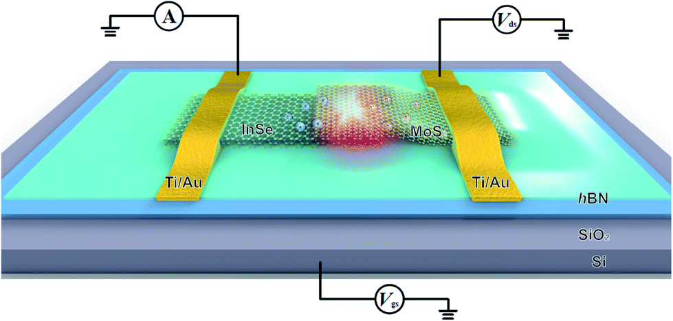 | ||
| Fig. 1 Schematic illustration of the p-MoS2/n-InSe vdWs heterostructure. | ||
Results and discussion
In this work, the p-type MoS2 and n-type InSe bulk crystals were grown via a chemical vapor transport (CVT) method. To p-type doping the MoS2, we used Nb as the dopant during the CVT process. To make a high-performance p-MoS2/n-InSe vdWs heterojunction, we first exfoliated the n-type InSe nanoflakes and p-type MoS2 nanoflakes on Si/SiO2 substrates in a glove box. Then, the heterostructure was stacked and encapsulated by top and bottom hBN nanoflakes using a spatially controlled dry transfer method,20 which guarantees the clean heterojunction interfaces and prevents contaminations from any polymers or solutions. After that, the top layer hBN was selectively etched and the Ti/Au (10/70 nm) contact electrodes were fabricated on both the InSe and MoS2 (Fig. 1) (see Method for details). hBN encapsulation avoids the degradation of InSe. To characterize the electrical properties of both p-MoS2 and n-InSe, as well as the contact behaviors of the Ti/Au electrodes, we fabricated field-effect transistors (FETs) of both p-MoS2 and n-InSe nanoflakes, with thickness of ∼15 nm and ∼15 nm, respectively (insets of Fig. 2b and d). The I–V curves of the few-layer InSe FET above turn-on back gate voltage (Vgs) show linear behavior at low source–drain bias (Vds) (Fig. 2a), confirming the ohmic contact characteristic between the low-work function Ti/Au (ΦTi = −4.33 eV) electrode and the n-type InSe. The source–drain current (Ids) saturates at a larger source–drain voltage (0.45 V). The channel current increases with increasing Vgs, indicating the n-type nature of the InSe. From the transfer curve (Fig. 2b), we can see that the threshold voltage and on/off ratio are about 22 V and >107 (see ESI S1†), respectively. The electron mobility (μe) and concentration (n2D) are estimated to be about 285 cm2 V−1 s−1 and ∼1012 cm−2, respectively, when the channel was turned on (see ESI S1†). Besides, the on-current of few-layer InSe increase by about two to three orders of magnitude compared with non-encapsulation ones (see ESI S3†). The I–V curves of the few-layer MoS2 FET show near-linear behaviors at different Vgs (Fig. 2c), because there exists kind of Schottky contact barrier at the interface of Ti/Au and the p-type MoS2. The channel current decreases with increasing Vgs, indicating the p-type nature of the MoS2. The channel cannot be fully depleted even when Vgs is as high as +80 V (Fig. 2d), indicating the heavily p-type doping nature of the MoS2. The hole mobility (μh) and concentration (p2D) is estimated to be about 1.7 cm2 V−1 s−1 and ∼3.03 × 1013 cm−2, respectively (see ESI S2†).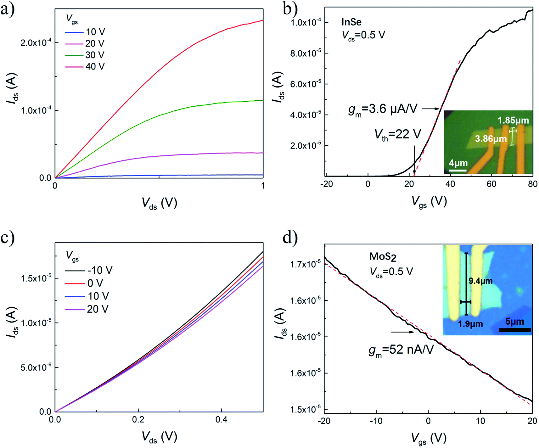 | ||
| Fig. 2 Electrical characterizations of the InSe and MoS2 nanoflakes. (a) The Ids versus Vds curves for the InSe FET under different Vgs. (b) The Ids versus Vgs curve of the InSe FET at Vds = 0.5 V. The red straight dash line shows the fitting result with channel transconductance (gm) of about 3.6 μA V−1 and turn-on threshold voltage (Vth) of 22 V. Inset: the optical image of the measured InSe FET with a channel length and width of 1.85 μm and 3.86 μm, respectively. (c) The Ids versus Vds curves for the MoS2 FET under different Vgs. (d) The Ids versus Vgs curve of the MoS2 FET at Vds = 0.5 V. The red straight dash line shows the fitting result with gm of about 52 nA V−1. Inset is the optical image of the measured MoS2 FET with a channel length and width of 1.9 μm and 9.4 μm, respectively. | ||
LED is a semiconductor device that converts electrical energy into light energy. The light emission mechanism from the p-MoS2/n-InSe LED can be qualitatively understood by studying the energy band diagram of the vdWs heterojunction, in which the Fermi levels of n-InSe and p-MoS2 coincide with each other in equilibrium state (Fig. 3a). Based on the depletion approximation, depletion layers with abrupt boundaries cause a built-in potential, while the semiconductors away from the depletion region boundaries are assumed to be electrically neutral. The determination of MoS2/InSe band alignment is based on the reported band gaps, affinities, and calculated work functions of MoS2 and InSe nanoflakes (see ESI S4†). Due to the difference in their band gaps (Eg) and electron affinities (χ), large conduction-band barrier (ΔEe ∼ 1.16 eV) and valence-band barrier (ΔEh ∼ 1.10 eV) are formed between MoS2 and InSe. Because the conduction band barrier is larger, with forward bias increasing, the valence band barrier will disappear first (Fig. 3b). At this stage, large amount holes will flow from the p-MoS2 to the n-InSe and recombine with the electrons at the InSe region. Therefore, the EL spectrum is determined by the band-edge emission of the InSe. Due to the degenerate p-doping nature of the MoS2, the EL intensity is limited by the electron concentration in InSe. The I–V curves of the vdWs heterojunction diode (Fig. 3d) show a clear rectifying behavior when the voltage changes from −2 V to 2 V. The turn-on voltage is ∼0.8 V. Due to the modest electron concentration of the InSe at zero gate voltage, the turn-on current of the diode is limited. When the back gate voltage increases from 0 V to 20 V, the on-current of the InSe/MoS2 heterojunction at Vds = 2 V increases from 2.78 μA to 19.56 μA, while the reverse current at Vds = −2 V increases from 4.71 nA to 78.23 nA, resulting the rectification ratio at ±2 V from 5.9 × 10² to 2.5 × 10². The I–V relationship of a p–n junction can be expressed as  , where I0 is the reverse saturation current, k is the Boltzmann constant, T is the temperature, q is the electron charge, and n is the ideality factor.21 For a p–n junction, the ideality factor n equals 2 when the recombination current dominates, and n equals 1 when the diffusion current dominates.21 By fitting the measured I–V curve at Vgs = 20 V with the above equation, we obtain n = 2.58. This ideality factor larger than 2 indicates that there exists recombination from other transport channels, which may be caused by the defects and impurities arising from the heavy doping.22 When the back-gate voltage is higher than 20 V and the source–drain bias is above the turn-on voltage, we can observe strong EL from the vdWs diode. Fig. 3e shows the room-temperature EL spectra under a forward bias of 9 V at various back-gate voltages. Under a positive back gate voltage, more electrons are injected from InSe and accumulated at the heterojunction interface to recombine with the injected holes, resulting in an enhanced EL emission. The EL spectra are dominated by an emission peaked around ∼1020 nm, coincident with the band-edge emission of the InSe nanoflake (see ESI S4†).
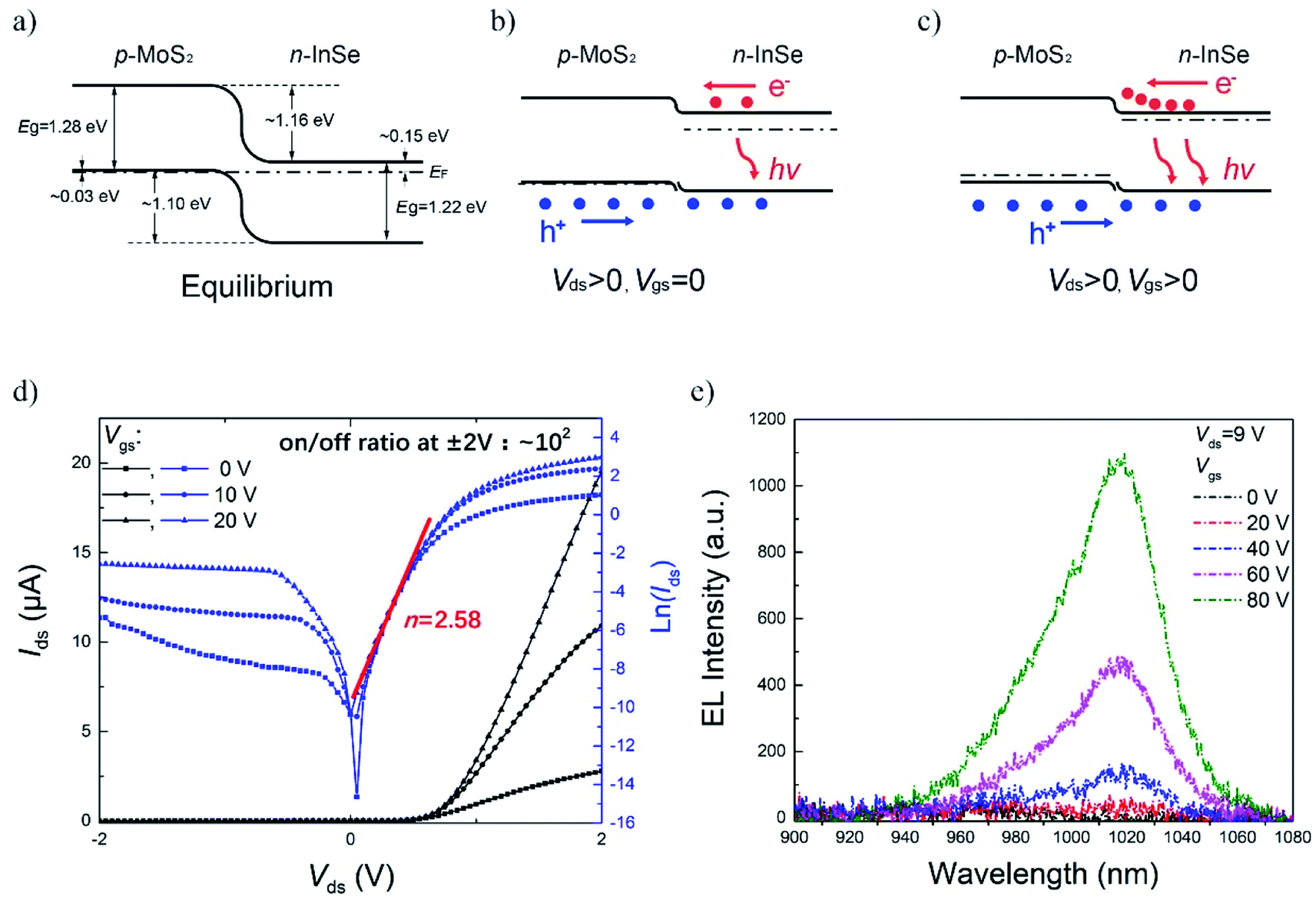 | ||
| Fig. 3 (a, b and c) The energy band diagrams of the p-MoS2/n-InSe heterojunction diode in equilibrium, under a forward bias and zero back gate voltage, and under a forward bias and positive back gate voltage, respectively. (d) Room-temperature I–V characteristics of the heterojunction diode depicted in the linear scale (black) and semi-log scale (blue), respectively. The red straight line shows the fitting result with an ideality factor n of about 2.58. (e) Room-temperature EL spectra under a forward source–drain bias of 9 V at various back-gate voltages. The EL intensity increases with the positive back-gate voltage, due to the increase of injected electrons from InSe. | ||
Photodetectors, which convert optical signals to electrical signals, are basic components in imaging techniques, optical communications, and future intra-chip optical interconnects.23 Herein, the p-MoS2/n-InSe heterojunction can serve as a photodiode, which can work without an external power supply. Upon light illumination, the photo-generated holes and electrons are driven towards the p-MoS2 and n-InSe, respectively, by the built-in field, resulting in a short-circuit current or a voltage drop on the external resistor. Under a standard solar illumination with a power density of 100 mW cm−2, the MoS2/InSe heterojunction exhibits good photovoltaic behavior (Fig. 4a), with a typical open-circuit voltage (Voc), short-circuit current density (Jsc), fill factor (FF), and energy conversion efficiency (η = FFJscVoc/Pin, where Pin is the illumination light power density) to be about 0.2 V, 1.17 mA cm−2, 50.4%, and 0.59%, respectively. The photosensitivity, defined as (Iphoto − Idark)/Idark, where Iphoto is the photocurrent and Idark is the dark current, is measured to be about 4.42 × 10³ at zero external bias. The photocurrent mapping at zero external bias under 633 nm laser excitation shows a uniform photoresponse at the heterostructure region (Fig. 4c), indicating the high-quality vdWs interface at the vertical stacked heterojunction.
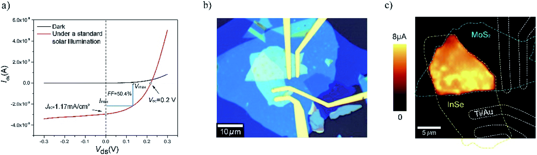 | ||
| Fig. 4 (a) The I–V curves of this p–n vdWs heterojunction diode in dark and under a standard solar illumination with a power density of 100 mW cm−2. (b) Optical image of the fabricated p–n vdWs heterojunction diode. (c) Photocurrent mapping of the p–n vdWs heterojunction under the excitation of a 633 nm laser with a power of 0.5 mW. | ||
Conclusion
In conclusion, we have fabricated all-2D vdWs hBN/p-MoS2/n-InSe/hBN vertical stacking heterostructure by the dry transfer method in a glove box. The type-II p-MoS2/n-InSe heterojunction diode exhibits a good rectification behavior and shows strong light emission at wavelength of ∼1020 nm under a forward bias exceeding the turn-on voltage and a positive back-gate voltage higher than 20 V. The EL intensity can be tuned by the back-gate voltage. Under simulated solar illumination, the vdWs p–n heterojunction exhibits a good photovoltaic behavior, with a typical Voc, Jsc, FF, and energy conversion of about 0.2 V, 1.17 mA cm−2, 50.4%, and 0.59%, respectively. The photosensitivity at zero external bias is about 4.42 × 10³. The photocurrent mapping shows a uniform photoresponse at the heterostructure region. The as-demonstrated all-2D vdWs heterojunction, which can work as both a light-emitting diode and a self-powered photodetector, may find applications in flexible wear, display, and optical communication fields, etc.Methods
Synthesis of p-type MoS2 bulk
To p-type dope the MoS2, we used Nb as the dopant during the CVT process. A horizontal three-zone furnace was utilized where the high (low) temperature zone was used as the reaction (growth) zone. Prior to the crystal growth, a quartz tube containing the iodine transport agent and the elements required for the doped crystals was evacuated to below 10−6 Torr and securely sealed. The purity of the source materials was Mo 99.99%, S 99.99%, and Nb 99.99%, with a molar ratio of Mo![[thin space (1/6-em)]](https://www.rsc.org/images/entities/char_2009.gif) :S:Nb equal to 1:2:0.005 for a nominal 0.5% Nb doping. The sealed quartz tube was then inserted into the three-zone furnace. In the beginning, the temperature of the growth zone was set to 1000 °C for 12 h to remove any possible residues. The process of the CVT was initiated with a temperature gradient varying from 1050 °C in the reaction zone to 935 °C in the growth zone over a distance of ∼30 cm, and the system was held in this condition over 500 h in order to provide sufficient diffusion and equilibration for the single-crystal synthesis.24
:S:Nb equal to 1:2:0.005 for a nominal 0.5% Nb doping. The sealed quartz tube was then inserted into the three-zone furnace. In the beginning, the temperature of the growth zone was set to 1000 °C for 12 h to remove any possible residues. The process of the CVT was initiated with a temperature gradient varying from 1050 °C in the reaction zone to 935 °C in the growth zone over a distance of ∼30 cm, and the system was held in this condition over 500 h in order to provide sufficient diffusion and equilibration for the single-crystal synthesis.24
Dry transfer method for assembly the hBN encapsulated p-MoS2/n-InSe heterostructures
The hBN/MoS2/InSe/hBN vertical stacked heterostructure was fabricated as follows: first, the hBN, MoS2, and InSe nanoflakes with appropriate thicknesses were exfoliated on Si/SiO2 substrates (the SiO2 layer was about 285 nm) (Fig. S3a–c in ESI S5†). Then the exfoliated hBN and MoS2 nanoflakes were picked up in sequence by a polydimethylsiloxane (PDMS) stamp covered by a layer of polypropylene carbonate (PPC) (Fig. S4a, b in ESI S6†). To avoid the degradation of InSe, the InSe related exfoliation and transfer processes were done in a glove box (O2, H2O < 0.1 ppm). The selected InSe nanoflake was picked up by the previously picked hBN/MoS2 heterostructure on PPC (Fig. S4c in ESI S6†) and transferred onto another hBN nanoflake on Si/SiO2 substrate (Fig. S4d in ESI S6†). The hBN encapsulated heterostructure was detached from PDMS/PPC at 60 °C and left on the device substrate (Fig. S4e in ESI S6†).Fabrication of the electrodes
The contact areas were patterned by electron-beam lithography, and the exposed top hBN layer was subsequently etched by reactive-ion etching using trifluoromethane and oxygen with flow rates of 20 sccm and 2 sccm for 2 min, respectively. Electron beam evaporation, and lift-off processes were used to fabricate the Ti/Au (10/70 nm) electrodes on both the InSe and MoS2 nanoflakes.Electrical measurements
All the electrical measurements were conducted with a semiconductor characterization system (Keithley 4200) under a probe station.PL and EL spectra characterizations
PL and EL spectra were recorded by a micro-zone confocal Raman spectroscope (HORIBA Jobin Yvon, LabRam HR 800) equipped with a color charge-coupled device (CCD) at room temperature. In the PL measurement, a 633 nm laser was used as the excitation and focused on the sample by a 50× objective (Olympus LMPlanFI IR). The EL and PL from devices were collected by the same objective.Photoresponse measurements
The photovoltaic measurements were conducted with a semiconductor characterization system (Keithley 4200) under a standard simulated solar illumination with a power density of 100 mW cm−2. The photocurrent mapping was recorded under the 633 nm laser illumination with a power of 0.5 mW using a micro-zone confocal Raman spectroscope (WITec alpha 300R). The photocurrent signal was collected and converted to a voltage signal by an amplifier with a magnification of 106, and recorded simultaneously with the scanning position information during the mapping process.Conflicts of interest
There are no conflicts to declare.Acknowledgements
This work was supported by the National Natural Science Foundation of China (No. 61521004, 61874003, and 61875001), and the National Key R&D Program of China (Grant No. 2018YFA0306900). D.-Y. L. acknowledges the financial support from the Ministry of Science and Technology of Taiwan, Republic of China under contract No. MOST 108-2221-E-018-010. K. W. and T. T. acknowledge support from the Elemental Strategy Initiative conducted by the MEXT, Japan and the CREST (JPMJCR15F3), JST.References
- K. S. Novoselov, V. Fal, L. Colombo, P. Gellert, M. Schwab and K. Kim, Nature, 2012, 490, 192 CrossRef CAS.
- N. O. Weiss, H. Zhou, L. Liao, Y. Liu, S. Jiang, Y. Huang and X. Duan, Adv. Mater., 2012, 24, 5782–5825 CrossRef CAS PubMed.
- F. Bonaccorso, Z. Sun, T. Hasan and A. Ferrari, Nat. Photonics, 2010, 4, 611 CrossRef CAS.
- F. Schwierz, Nat. Nanotechnol., 2010, 5, 487 CrossRef CAS.
- P. Avouris, Nano Lett., 2010, 10, 4285–4294 CrossRef CAS.
- L. Britnell, R. Ribeiro, A. Eckmann, R. Jalil, B. Belle, A. Mishchenko, Y.-J. Kim, R. Gorbachev, T. Georgiou and S. Morozov, Science, 2013, 340, 1311–1314 CrossRef CAS.
- H. Fang, S. Chuang, T. C. Chang, K. Takei, T. Takahashi and A. Javey, Nano Lett., 2012, 12, 3788–3792 CrossRef CAS.
- D. J. Groenendijk, M. Buscema, G. A. Steele, S. Michaelis de Vasconcellos, R. Bratschitsch, H. S. van der Zant and A. Castellanos-Gomez, Nano Lett., 2014, 14, 5846–5852 CrossRef CAS.
- J. S. Ross, P. Klement, A. M. Jones, N. J. Ghimire, J. Yan, D. Mandrus, T. Taniguchi, K. Watanabe, K. Kitamura and W. Yao, Nat. Nanotechnol., 2014, 9, 268 CrossRef CAS.
- Y. Zhang, T. Oka, R. Suzuki, J. Ye and Y. Iwasa, Science, 2014, 344, 725–728 CrossRef CAS.
- Y. Zhou, Y. Nie, Y. Liu, K. Yan, J. Hong, C. Jin, Y. Zhou, J. Yin, Z. Liu and H. Peng, ACS Nano, 2014, 8, 1485–1490 CrossRef CAS.
- J. Pu, Y. Yomogida, K.-K. Liu, L.-J. Li, Y. Iwasa and T. Takenobu, Nano Lett., 2012, 12, 4013–4017 CrossRef CAS.
- X. Hong, J. Kim, S.-F. Shi, Y. Zhang, C. Jin, Y. Sun, S. Tongay, J. Wu, Y. Zhang and F. Wang, Nat. Nanotechnol., 2014, 9, 682 CrossRef CAS.
- Y. Gong, J. Lin, X. Wang, G. Shi, S. Lei, Z. Lin, X. Zou, G. Ye, R. Vajtai and B. I. Yakobson, Nat. Mater., 2014, 13, 1135 CrossRef CAS.
- G. W. Mudd, S. A. Svatek, T. Ren, A. Patanè, O. Makarovsky, L. Eaves, P. H. Beton, Z. D. Kovalyuk, G. V. Lashkarev and Z. R. Kudrynskyi, Adv. Mater., 2013, 25, 5714–5718 CrossRef CAS.
- D. A. Bandurin, A. V. Tyurnina, L. Y. Geliang, A. Mishchenko, V. Zólyomi, S. V. Morozov, R. K. Kumar, R. V. Gorbachev, Z. R. Kudrynskyi and S. Pezzini, Nat. Nanotechnol., 2017, 12, 223 CrossRef CAS.
- Z. Chen, J. Biscaras and A. Shukla, Nanoscale, 2015, 7, 5981–5986 RSC.
- G. W. Mudd, S. A. Svatek, L. Hague, O. Makarovsky, Z. R. Kudrynskyi, C. J. Mellor, P. H. Beton, L. Eaves, K. S. Novoselov and Z. D. Kovalyuk, Adv. Mater., 2015, 27, 3760–3766 CrossRef CAS.
- S. R. Tamalampudi, Y.-Y. Lu, R. U. Kumar, R. Sankar, C.-D. Liao, K. B. Moorthy, C.-H. Cheng, F. C. Chou and Y.-T. Chen, Nano Lett., 2014, 14, 2800–2806 CrossRef CAS.
- L. Wang, I. Meric, P. Huang, Q. Gao, Y. Gao, H. Tran, T. Taniguchi, K. Watanabe, L. Campos and D. Muller, Science, 2013, 342, 614–617 CrossRef CAS.
- S. Sze and C. A. Mead, Analog VLSI and Neural Systems, Addison-Wesley, Reading, MA, 1989, p. 36 Search PubMed.
- P. Gehring, R. Urcuyo, D. L. Duong, M. Burghard and K. Kern, Appl. Phys. Lett., 2015, 106, 233110 CrossRef.
- Z. Gao, W. Jin, Y. Zhou, Y. Dai, B. Yu, C. Liu, W. Xu, Y. Li, H. Peng and Z. Liu, Nanoscale, 2013, 5, 5576–5581 RSC.
- J. Suh, T.-E. Park, D.-Y. Lin, D. Fu, J. Park, H. J. Jung, Y. Chen, C. Ko, C. Jang and Y. Sun, Nano Lett., 2014, 14, 6976–6982 CrossRef CAS PubMed.
Footnote |
| † Electronic supplementary information (ESI) available. See DOI: 10.1039/c9ra06667e |
| This journal is © The Royal Society of Chemistry 2019 |