 Open Access Article
The surface passivation of Ge(100) and Ge(111) anodes in Ge–air batteries with different doping types and concentrations†
Yingjian Yu *abc,
Danshuo Chena,
Shaoshuai Gaoa,
Jian Huanga,
Sujuan Hud,
Hai Yangab and
Guojun Jinab
aCollege of Physics Science and Technology, Kunming University, Kunming, Yunnan 650214, China. E-mail: yuyingjiankmu@163.com
bNational Laboratory of Solid State Microstructures, Nanjing University, Nanjing, 210093, China
cFujian Province Key Laboratory of Semiconductor Materials and Application, Xiamen University, Xiamen, Fujian 361005, China
dDepartment of Chemistry, Kunming University, Kunming, Yunnan 650214, China
First published on 2nd December 2019
Abstract
The surface passivation of Ge(100) and Ge(111) anodes in Ge–air batteries with different doping types and concentrations is analyzed by density function theory (DFT) calculations. Compared with Ge(111) anodes, the surface passivation is restrained on Ge(100) anodes as they have larger binding energies with GeO2 layers. Meanwhile, doping would hinder the formation of a GeO2 layer on Ge anodes, especially for p-type doping, like B. The dissimilarities of the electrostatic potential differences and projected local density of states between the p-type Ge(100)/GeO2 and Ge(111)/GeO2 also reveal the origins of their distinct performances in Ge–air batteries. Furthermore, the I–V curves show that the Ge(100)/GeO2/Ge(100) device has a higher current than the Ge(111)/GeO2/Ge(111) device. This work would help to fundamentally comprehend the different electrochemical properties of Ge–air batteries with different orientations and doping and provide guidelines for the design of Ge anodes in Ge–air batteries.
Introduction
In recent decades, the energy revolution has moved to the top of the agenda around the world due to the shortage of fossil fuels and severe climate change. Nowadays, green energy systems, e.g. lithium ion batteries,1 fuel cells,2 and solar cells,3 are playing a critical role in human life. Among them, air batteries, with high energy/power densities and widely distributed raw materials, can be potentially applied to automotive vehicles, traffic signal systems, offshore power facilities and portable power supplies.4,5 What makes air batteries distinctive is their negligible cathode volumes since the oxidant (oxygen) can be directly obtained from the air. Metal–air batteries have been extensively studied, such as Li–air batteries,6 Al–air batteries7 and Zn–air batteries;8 however, challenges like dendrite formation still exist.9 Germanium has been introduced as the anode material in semiconductor air batteries, and exhibits high capacities and ideal safety.10–12 During the discharge process, the germanium oxidation reaction and the oxygen reduction reaction (ORR) occur in the anode and cathode. Meanwhile, the germanium hydroxide dehydrates to its oxide, which would passivate the Ge anode surface and prevent further discharging. Eventually, the Ge/GeO2 interface forms.10–12Anode discharge:
| Ge + 4OH− → Ge(OH)4 + 4e− | (1) |
ORR:
| O2 + 2H2O + 4e− → 4OH− | (2) |
Surface passivation:
| Ge(OH)4 → GeO2 + 2H2O | (3) |
Experiments have shown that the performances of Ge–air batteries are significantly affected by the doping and crystal orientations of Ge anodes.11,12 In general, p-type Ge anodes with the (100) crystal indice show better discharge properties. To further improve the fundamental understanding of the physics and chemistry of the Ge–air batteries, theoretical investigations on the surface passivation and properties of the Ge/GeO2 interface in the cell become the urgent demands, which may provide guidelines to design the Ge anode.
In this work, atomic model structures of the Ge/GeO2 interfaces with different Ge crystal orientations, doping types and concentrations were constructed and density functional theory (DFT) calculations were conducted. It was found that the GeO2 layer prefer to form on the Ge(111) rather than Ge(100), and p-doped Ge may resist the surface passivation more obviously. The electrostatic difference potentials and projected local density of states of the Ge(100)/GeO2 and Ge(111)/GeO2 interfaces were also calculated. Moreover, the I–V curves show that the Ge(100)/GeO2/Ge(100) device has a higher current than the Ge(111)/GeO2/Ge(111) device. This work would help to understand the different electrochemical properties of Ge–air batteries with different orientations and doping fundamentally.
Method
DFT calculations13,14 within the generalized gradient approximation (GGA) were performed using the Atomistix ToolKit (ATK) code from QuantumWise.15 The exchange–correlation functional of Perdew–Burke–Ernzerhof (PBE) was used for the GGA calculations.16,17 In the calculations of the models of Ge/GeO2 interfaces, a 4 × 4 × 1 k-point mesh was used. The presented models were structurally relaxed within the force tolerance of 0.01 eV Å−1. The thickness of the vacuum layer is 10 Å. The convergence tests of the k-point mesh and the thickness of the vacuum layer are shown in Fig. S1 and S2 in the ESI.† The methodology on the electrostatic potential difference, projected local density of states (PLDOS), transmission spectra and IV curves are detailed in ESI.†Results and discussion
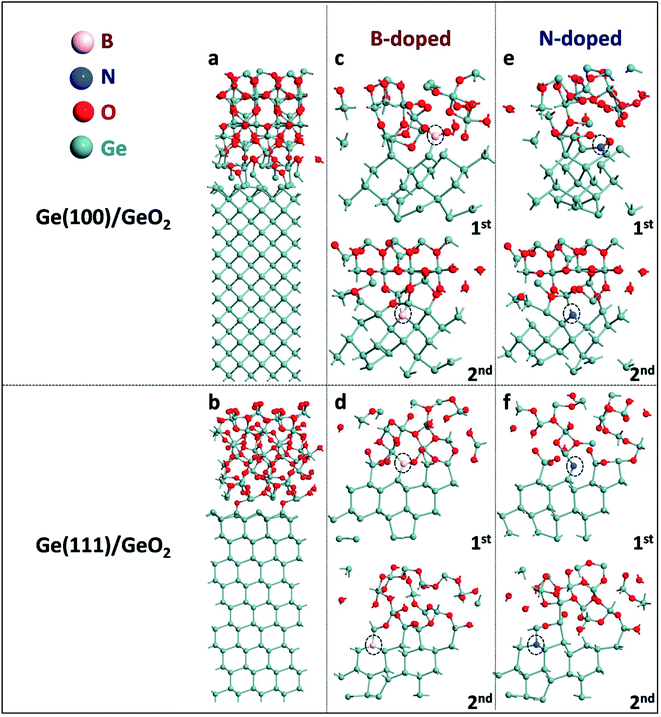
Atomic configurations of Ge(100)/GeO2 and Ge(111)/GeO2 models are shown in Fig. 1a and b. In the Ge(100)/GeO2 model, the 3-fold bonded Ge and 3-fold O can be visualized at the interface, with the average Ge–O bond length of ∼2.02 Å and average Ge–O–Ge bond angle of ∼116.84°. For comparison, in the Ge(111)/GeO2 model, the Ge slabs and GeO2 layer are linked by the 2-fold O. The average Ge–O bond length is ∼1.97 Å and average Ge–O–Ge bond angle is ∼110.27°, which are both smaller than those in the Ge(100)/GeO2 model, indicating the stronger coalescent of the Ge(111)/GeO2 interface. To describe it quantitatively, the binding energy of Ge/GeO2 interfaces is calculated by the definition of| Eb,Ge/GeO2 = (EGe/GeO2 − EGe − EGeO2)/n, | (4) |
| Ge(100)/GeO2 | Ge(111)/GeO2 | |||
|---|---|---|---|---|
| None | 1.61 | 0.53 | ||
| Doped | B | N | B | N |
| 1st | 5.82 | 5.39 | 5.39 | 5.38 |
| 2nd | 5.63 | 5.38 | 5.32 | 5.11 |
In experiments, Ge anodes in Ge–air batteries are usually doped, thus the effects of the doping types on the binding energies are also explored in the Ge(100)/GeO2 and Ge(111)/GeO2 models. As exhibited in Fig. 1c and d, one Ge atom in the first and second slab is substituted by one B atom, respectively. In the Ge(100)–B/GeO2 model in Fig. 1c, the B atom in the first slab forms two B–O bonds with lengths of 1.38 and 1.31 Å and one B–Ge bond with the length of 2.14 Å. The binding energy increases to 5.82 eV dramatically compared with that of Ge(100)/GeO2 model without doping, suggesting that the B-doped Ge(100) anode has a positive effect to avoid the surface passivation.11 In the case of the substitution in the second slab, the fourfold coordinated B atom has four bonds with Ge with an average length of 2.13 Å. The binding energy also increases to 5.63 eV, evidencing the conclusion above. Moreover, it can be concluded that the binding energy is more sensitive to the doping closer to the Ge(100)/GeO2 interface with a larger binding energy. Similar phenomena can be found in the case of Ge(111)/GeO2 interface as shown in Fig. 1d. The B atom in the first slab forms two B–Ge bonds with lengths of 2.09 and 2.16 Å and one B–O bond with the length of 1.31 Å. For B doped in the second slab, the fourfold coordinated B atom can be visualized which has four bonds with Ge with an average length of 2.16 Å. In both cases of Ge(111)–B/GeO2, the binding energies increase apparently compared with those of Ge(111)/GeO2 without doping, suggesting that the B-doped Ge(111) anode is also beneficial to prevent the severe passivation on the surface of anode. It is deserved to mention that the binding energies in the Ge(100)–B/GeO2 interfaces are both larger than those in the corresponding Ge(111)–B/GeO2, which conform to the comparison between Ge(100)/GeO2 and Ge(111)/GeO2 models, theoretically illustrating the better experimental electrochemical properties of Ge(100) anodes.
Besides doping by the B atom, various kinds of doping by the N atom are also analyzed in the Ge(100)/GeO2 and Ge(111)/GeO2 models as exhibited in Fig. 1e and f. In Fig. 1e, the N atom in the first slab forms one N–O bond (1.24 Å) and two N–Ge bonds with lengths of 2.07 and 2.12 Å after relaxation; the N atom in the second slab has three N–Ge bonds with an average length of 1.98 Å. In Fig. 1f, the N atom in the first slab forms two N–Ge bonds (1.84 Å and 1.83 Å); the fourfold coordinated N atom in the second slab has four N–Ge bonds with an average length of 2.10 Å.
According to the corresponding binding energies of those models in Table 1, reasonable conclusions can be concluded: (i) doping by the N atom also helps to alleviate the passivation on the Ge(100) and (111) surfaces; (ii) the binding energies are more sensitive to the N/B atom closer to the Ge/GeO2 interface; (iii) the B-doped Ge anode is a better candidate for Ge–air batteries than the N-doped Ge anode. Furthermore, all the Ge(100) substrates exhibit larger binding energies than corresponding Ge(111) substrates, theoretically revealing that Ge(100) anodes would show better electrochemical properties than Ge(111) anodes. That phenomenon has already been found in experiments by Ocon.12
The bonds formed by heteroatoms in the first slab are analyzed by charge density difference as shown in Fig. 2. Both in the Ge(100)/GeO2 and Ge(111)/GeO2 models, there are charge transfer of ∼0.2 eÅ−3 to form the B–Ge bonds and N–Ge bonds. The charge transfer between the N and O atom is more distinct (∼0.3 eÅ−3), indicating the stronger binding of the interface induced by the N doping. It can be found that the dopants like B and N near the Ge/GeO2 interface would affect the configuration of the interface obviously by forming the B–O, B–Ge, N–O and N–Ge bonds. Also, the charge transfer would be affected by the introducing of dopants. As a result, the binding energy would be significantly impacted by the dopant in the first or second slab for both Ge(100) and Ge(111) orientations.
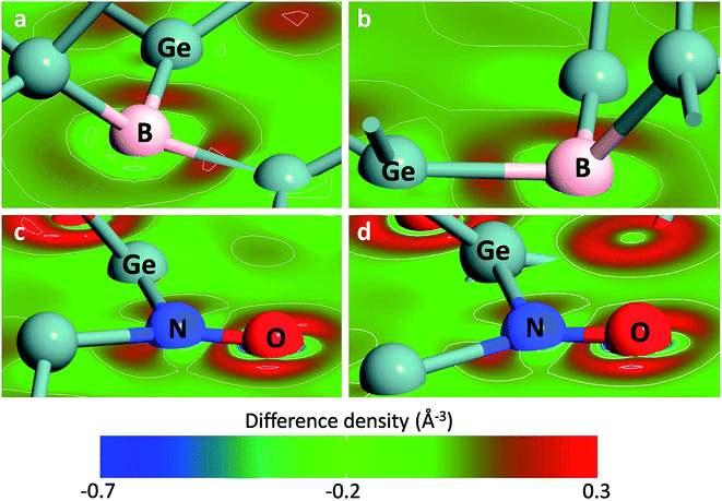 | ||
| Fig. 2 The charge density difference of B-doped (a) Ge(100)/GeO2 and (b) Ge(111)/GeO2 interfaces and N-doped in the (c) Ge(100)/GeO2 and (d) Ge(111)/GeO2 interfaces. | ||
Since doping by B leads to better performances, for simplicity, the binding energies of p-type Ge(100)/GeO2 and p-type Ge(111)/GeO2 models with various doping concentrations are calculated to strength the viewpoint, as shown in Fig. 3. In experiments, the Ge wafers with doping concentrations of 1014, 1016 and 1018 are usually considered to be slightly, medium and heavily doped; so the doping concentrations larger than 1014 are investigated. Using the ATK code, different doping concentrations can be modeled by doping charge to the selected Ge atoms without explicitly introducing dopant atoms (detailed in Fig. S4†). In the full range of 1014 to 1021, the p-type Ge(100)/GeO2 models have larger binding energies than those of p-type Ge(111)/GeO2 models and Ge(100)/GeO2 models without doping, which verify the conclusion above. It cannot be neglected that the binding energies decrease markedly when the Ge substrates are doped with the concentration of 1021. Those relaxed models have the elongation of ∼2% along the c axis than the models with the doping concentration of 1016. Meanwhile, the p-type Ge(111) with the doping concentration of 1021 are linked with GeO2 layer by only twofold O atoms; however, both twofold and threefold O atoms can be seen across the interface in Fig. 4b (1016). Those differences between the models with doping concentrations of 1016 and 1021 may lead to the variations of the binding energies.
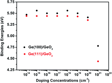 | ||
| Fig. 3 The binding energies of p-type Ge(100)/GeO2 and p-type Ge(111)/GeO2 with various doping concentrations. | ||
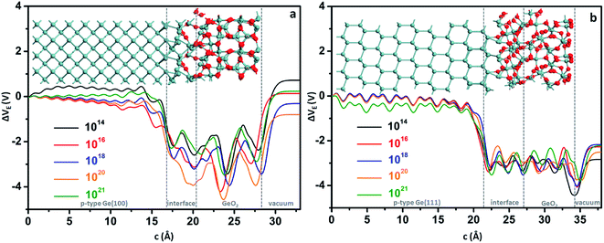
Besides the binding energies, the electrostatic difference potentials are analyzed to disclose the differences between the p-type Ge(100)/GeO2 and p-type Ge(111)/GeO2 interfaces as shown in Fig. 4. Similar offsets of 3–4 V can be found across the p-type Ge/GeO2 interfaces in Fig. 4a and b, which result from the differences in electronegativities between Ge and O.19 It is worth mentioning that the electrostatic difference potentials rise apparently across the GeO2/vacuum in Fig. 4a; however, the rising in Fig. 4b is not that obvious. The differences in the electrostatic difference potentials imply that it would be favourable for the electrons to transfer from the Ge(100) anode to the air cathode via the GeO2 passivation layer in discharge processes.
The projected local density of states (PLDOS) of the p-type Ge(100)/GeO2 and p-type Ge(111)/GeO2 with the doping concentration of 1016 are displayed in Fig. 5a and b. The PLDOS offers a highly useful visualization of the band diagram of the interface. It nicely shows the electronic structure across the full length of the interface and the band gaps of the left and right side of the Ge/GeO2 interface can be visualized clearly. The similar band gap of ∼0.55 eV can be found in the regions of Ge(100) and Ge(111) substrate; however, a more distinct valence band demarcation can be visualized in the Ge(111)/GeO2 model with a larger band gap of ∼2.58 eV in the region of GeO2 layer than that of ∼2.40 eV in the Ge(100)/GeO2 model. The larger band gap would probably hinder the electron transfer and result in a higher resistivity.12 The band gap of Ge measured at 300 K is 0.66 eV (ref. 20) and that of GeO2 is 4.68 eV.21 Our values are smaller than the experimental data due to the well-known underestimation of conduction band state energies in DFT calculations. The PBE has been widely used in the theoretical investigation of the Ge/GeO2 interface.17,22,23 In this work, the calculated band gap of Ge is only 0.11 eV smaller than the experimental value, and this band gap is larger than that in the previous work (0.4 eV).17 Given the well-known underestimation of the band gap with PBE, the calculated value in this work is acceptable and reasonable.
 | ||
| Fig. 5 The projected local density of states of the (a) p-type Ge(100)/GeO2 and (b) p-type Ge(111)/GeO2 with the doping concentration of 1016. | ||
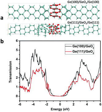
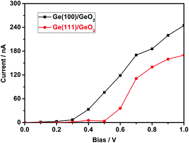
To investigate the transmission spectra and I–V characteristics of the Ge(100)/GeO2 and Ge(111)/GeO2 interfaces, the devices of Ge(100)/GeO2/Ge(100) and Ge(111)/GeO2/Ge(111) are constructed as shown in Fig. 6a. Smaller models are used here because the calculations of the transmission spectra and I–V curves need much more time than the preceding DFT analysis. The energy gaps of the two models are ∼2.0 eV as exhibited in Fig. 6b. Generally, the transmission of the Ge(100)/GeO2 interface is higher than that of the Ge(111)/GeO2. For the Ge(100)/GeO2 interface, the transmission is higher than 2 mainly at the energy ranges of approximately −4.3 to −2.0 eV and 2.2–4.6 eV. For the Ge(111)/GeO2 interface, the corresponding energy range is about −4.2 to −2.2 eV. Furthermore, the I–V curves are calculated as exhibited in Fig. 7. Since the operating voltages of Ge(100) and Ge(111) anodes were 0.92 and 0.87 V in a previous work,12 the voltage bias of 0–1 V was calculated. The current is relatively low when the voltage bias is smaller than 0.3 V, which is corresponded to the half of the band gap of Ge. When the voltage bias comes to 1 V, the current of Ge(100)/GeO2/Ge(100) device reaches to 245 nA, which is much higher than that of Ge(111)/GeO2/Ge(111) device (170 nA), evidencing that the flow of electrons is affected by the crystal structure of the anode.12 Furthermore, the configurations, transmission and I–V curves of Ge(100)/GeO2 with oxygen vacancies are shown in Fig. S5.† As shown in Fig. S5b,† the transmission spectrum is similar to that of the Ge(100)/GeO2 model without O vacancies. In Fig. S5c,† the current is 211 nA at the voltage bias of 1 V, which is a little smaller than that of the Ge(100)/GeO2 interface.
Conclusions
In conclusion, the Ge(100)/GeO2 and Ge(111)/GeO2 models are constructed to analyze the properties of the anodes interfaces in Ge–air batteries. By calculating the binding energies with the density function theory, Ge(100) anodes are found to be better candidates for Ge–air batteries than Ge(111) anodes. Meanwhile, doping, especially the p-type doping like B, would result in larger binding energies and relieve the surface passivation caused by the formation of GeO2 layers on Ge surfaces. Moreover, the band gap of GeO2 in the p-type Ge(100)/GeO2 model is smaller than that in the p-type Ge(111)/GeO2 model, which would improve the electron transfer from anodes to cathodes in discharge processes. Finally, the Ge(100)/GeO2/Ge(100) device exhibits a higher current than the Ge(111)/GeO2/Ge(111) device. This work would help to explore the origins of the different electrochemical properties of Ge–air batteries with different orientations and doping fundamentally and provide guidelines for the design of Ge anodes in Ge–air batteries.Conflicts of interest
There are no conflicts to declare.Acknowledgements
This work is financially supported by the National Nature Science Foundation of China (Grant No. 61904073 and No. 11264022), the Science Foundation of Yunnan Provincial Education Department (2018JS392), the Spring City Plan – Special Program for Young Talents, the Science Foundation of National Laboratory of Solid State Microstructures (M31036 and M31020), the Talents Introduction Project of Kunming University (YJL18008 and YJL16003), the Open Project Program of the Fujian Province Key Laboratory of Semiconductor Materials and Application, the Yunnan Local College Applied Basic Research Projects (Grant No. 2017FH001-001), and the Applied Basic Research Programs of Yunnan Science and Technology Department (2017FD085).References
- M. Li, J. Lu, Z. Chen and K. Amine, 30 years of lithium-ion batteries, Adv. Mater., 2018, 30(33), 1800561 CrossRef PubMed.
- D. R. Dekel, Review of cell performance in anion exchange membrane fuel cells, J. Power Sources, 2018, 375, 158–169 CrossRef CAS.
- B. Salhi, Review of recent developments and persistent challenges in stability of perovskite solar cells, Renewable Sustainable Energy Rev., 2018, 90, 210–222 CrossRef CAS.
- X. Zhang, X. Wang, Z. Xie and Z. Zhou, Recent progress in rechargeable alkali metal-air batteries, Green Energy & Environment, 2016, 1, 4–17 Search PubMed.
- Y. Li and J. Lu, Metal-air batteries: will they be the future electrochemical energy storage device of choice?, ACS Energy Lett., 2017, 2, 1370–1377 CrossRef CAS.
- M. Asadi, B. Sayahpour, P. Abbasi, A. Ngo, K. Karis, J. Josiaari, C. Liu, B. Narayanan, M. Gerard, P. Yaeael, X. Hu, A. Mukherjee, K. Lau, R. Assary, F. Khalili-Araghi, R. Klie, L. Crutiss and A. Salehi-Khojin, A lithium-oxygen battery with a long cycle life in an air-like atmosphere, Nature, 2018, 555, 502–506 CrossRef CAS PubMed.
- J. Ryu, M. Park and J. Cho, Advanced technologies for high-energy aluminum-air batteries, Adv. Mater., 2018, 1804784 Search PubMed.
- X. Fan, J. Liu, Z. Song, X. Han, Y. Deng, C. Zhong and W. Hu, Porous nanocomposite gel polymer electrolyte with high ionic conductivity and superior electrolyte retention capability for long-cycle-life flexible zinc-air batteries, Nano Energy, 2019, 56, 454–462 CrossRef CAS.
- D. Lin, Y. Liu and Y. Cui, Reviving the lithium metal anode for high-energy batteries, Nat. Nanotechnol., 2017, 12, 194–206 CrossRef CAS PubMed.
- J. Ocon, J. Kim, S. Uhm, B. Mun and J. Lee, An etched nanoporous Ge anode in a novel metal-air energy conversion cell, Phys. Chem. Chem. Phys., 2013, 15, 6333–6338 RSC.
- J. Ocon, J. Kim, G. Abrenica, J. Lee and J. Lee, Quasi-perpetual discharge behavior in p-type Ge-air batteries, Phys. Chem. Chem. Phys., 2014, 16, 22487–22494 RSC.
- J. Ocon, G. Abrenica and J. Lee, High-power-density semiconductor-air batteries based on p-type germanium with different crystal orientations, ChemElectroChem, 2016, 3, 242–246 CrossRef CAS.
- M. C. Payne, M. P. Teter, D. C. Allan, T. A. Arias and J. D. Joannopoulos, Iterative minimization techniques for ab initio total-energy calculations: molecular dynamics and conjugate gradients, Rev. Mod. Phys., 1992, 64, 1045–1097 CrossRef CAS.
- M. Houssa, G. Pourtois, M. Caymax, M. Meuris, M. M. Heyns, V. V. Afanas’ev and A. Stesmans, Ge dangling bonds at the (100) Ge/GeO2 interface and the viscoelastic properties of GeO2, Appl. Phys. Lett., 2008, 93, 161909 CrossRef.
- Atomistix Toolkit (ATK), http://www.quantumwise.com.
- J. P. Perdew, K. Burke and M. Ernzerhof, Generalized Gradient Approximation Made Simple, Phys. Rev. Lett., 1996, 77, 3865–3868 CrossRef CAS PubMed.
- P. Broqvist, J. Binder and A. Pasquarello, Atomistic model structure of the Ge(100)-GeO2 interface, Microelectron. Eng., 2009, 86, 1589–1591 CrossRef CAS.
- S. D. Elliott and J. C. Greer, Structural and energetic origin of defects at the interface between germanium and a high-k dielectric from first principles, Appl. Phys. Lett., 2011, 98, 082904 CrossRef.
- P. Broqvist, J. Binder and A. Pasquarello, Band offsets at Ge/GeO2 interfaces: Effect of different interfacial bonding patterns, Microelectron. Eng., 2011, 88, 1467–1470 CrossRef CAS.
- W. L. Hansen and E. E. Haller, Germanium, Encyclopedia of Applied Physics, 1993, vol. 7 Search PubMed.
- M. Stapelbroek and B. D. Evans, Exciton structure in the U.V.-absorption edge of tetragonal GeO2, Solid State Commun., 1978, 25, 959–962 CrossRef CAS.
- P. Broqvist, A. Alkauskas and A. Pasquarello, Defect levels of dangling bonds in silicon and germanium through hybrid functional, Phys. Rev. B: Condens. Matter Mater. Phys., 2008, 78, 075203 CrossRef.
- J. F. Binder, P. Broqvist and A. Pasquarello, First principles study of substoichiometric germanium oxides, Microelectron. Eng., 2009, 86, 1760–1762 CrossRef CAS.
Footnote |
| † Electronic supplementary information (ESI) available. See DOI: 10.1039/c9ra06725f |
| This journal is © The Royal Society of Chemistry 2019 |

