Disordered layers on WO3 nanoparticles enable photochemical generation of hydrogen from water†
Luyang
Wang
a,
Chui-Shan
Tsang
a,
Wei
Liu
a,
Xiandi
Zhang
a,
Kan
Zhang
b,
Enna
Ha
a,
Wai-Ming
Kwok
 a,
Jong Hyeok
Park
 b,
Lawrence Yoon
Suk Lee
 *a and
Kwok-Yin
Wong
 *a
*a
aDepartment of Applied Biology and Chemical Technology, The State Key Laboratory of Chemical Biology and Drug Discovery, The Hong Kong Polytechnic University, Hung Hom, Hong Kong SAR, China. E-mail: lawrence.ys.lee@polyu.edu.hk; kwok-yin.wong@polyu.edu.hk
bDepartment of Chemical and Biomolecular Engineering, Yonsei University, 50 Yonsei-ro, Seodaemun-gu, Seoul 120-749, Republic of Korea
First published on 23rd November 2018
Abstract
Tailored defects on a semiconductor surface can provide active catalytic sites and effectively tune the electronic structure for suitable optical properties. Herein, we report that surface modification of WO3 with a disordered layer enables the photochemical hydrogen production from water. A simple room temperature solution process with lithium-ethylenediamine (Li-EDA) alters the surface of WO3 with localized defects that form a thin disordered layer. Both structural and optical characterization reveal that such a disordered layer induces an upshift in the Fermi level and the elevation of the conduction band of WO3 above the hydrogen reduction potential. Using an alkaline sacrificial agent, Li-EDA treated WO3 shows a co-catalyst-free photochemical hydrogen evolution rate of 94.2 μmol g−1 h−1 under simulated sunlight. To the best of our knowledge, this is the first example of using WO3 as a direct photocatalyst for hydrogen generation from water via simple surface defect engineering.
Introduction
Solar energy-driven hydrogen generation from water can offer a clean and sustainable solution to address the growing energy demand with reduced fossil fuel dependence and associated environmental issues.1–3 In recent years, much effort has been made to develop effective photocatalysts based on abundant and economical elements.4–7 However, their overall photocatalytic efficiencies are insufficient to replace those made of noble metals. Tuning the light absorption, charge kinetics, and surface activity of catalysts can elevate the photocatalytic performance, but it is still challenging to achieve the activity of noble metal-based ones.Semiconductor metal oxides, with advantages of natural abundance, chemical stability, and low cost, have been widely used as photocatalysts and electrode materials for energy conversion and storage devices.8 Both electronic and optical properties of metal oxides can be regulated by the type and population of defect introduced. The creation of intrinsic defects, such as oxygen vacancies, and doping of low valence metal centers or non-metal atoms are the most commonly used defect engineering methods for tailoring the photocatalytic activity.9–12 In particular, oxygen vacancies are known to serve as shallow donors for metal oxides, such as TiO2,13 WO3,14 and SnO2.15 It is generally accepted that the increased carrier density improves the electrical conductivity and facilitates the charge transfer at the interface between the metal oxide and substrate.
The introduced defects can be extended to form an internal boundary7 or even a disordered layer,10 and are relatively less studied than atomic point defects. A surface disordered layer arises from the large amount of lattice disorder on the crystalline surface after being treated under reducing conditions. Such layers usually contain a significant amount of oxygen vacancies and low valence metal centers (self-doped), which may create mid-gap states below the Fermi level of the metal oxide.16 The mid-gap states form a continuum that extends to and overlaps with the conduction band (CB) or merges with the valence band (VB). This can effectively reduce the band gap and enhance the light absorption in the visible and near-IR regions.17,18 These extended energy states and the newly produced energy levels may become dominant for optical excitation and relaxation, and thus new applications may be obtained. Furthermore, the localized holes generated in the mid-gap state of the disordered layer efficiently inhibit the charge recombination,16,19–22 where the low valence metal centers act as trapping sites for photogenerated carriers.
The pioneering work on black TiO2 with disordered surface layers16 demonstrated a significant enhancement in the photocatalytic hydrogen evolution reaction (HER) rate and has sparked the investigations on creating disordered layers in other metal oxides, including Fe2O3,23 ZnO,24 BiVO4,25 and WO3.26,27 Among them, tungsten oxide (WO3) is an important n-type semiconductor with various applications ranging from dye-sensitized solar cells28 to electrochromic devices,29 gas sensors,30 and photoelectrochemical water splitting,31 owing to its low cost and good conductivity. With a desirable bandgap energy (2.5–2.8 eV) for capturing visible light and a number of stable oxygen-deficient sub-stoichiometric structures (WO3−x, where 0 < x ≤ 0.28) available, WO3 is one of the most attractive candidates for photocatalytic water splitting.32 Nonetheless, restricted by its intrinsic electronic structure, WO3 is only suitable for water oxidation.33 The position of the valence band maximum (VBM) of WO3 is located at a relatively high energy level (3.0 eV vs. reversible hydrogen electrode, RHE), whereas the conduction band minimum (CBM) lies at a position lower than the hydrogen reduction potential (0 V vs. RHE).
Recently, a thin disordered layer on the WO3 surface has been reported to significantly increase the charge carrier density and facilitate the interface charge transfer, thus improving the charge separation efficiency and conductivity in photoelectrocatalytic water oxidation.26,27 Localized surface atomic disorder was also engaged in turning the inert WO3 into an active electrocatalyst for hydrogen generation from acidic water.34 Nevertheless, it is still challenging to trigger solar water reduction using WO3 and the effect of the surface disordered layer on the band structure of WO3 has not been clearly understood yet. Herein, we demonstrate that a simple room-temperature solution processing method can modify the surface morphology and electronic structure of WO3 to enable the unprecedented capability of facilitating the photocatalytic HER without a co-catalyst. Using Li-ethylenediamine (Li-EDA) as a disordering agent, a surface disordered layer was successfully created on the crystalline WO3 nanoplates (see Scheme 1 for synthetic schematics). Experimental results confirm the formation of a mid-gap state that causes a blue-shift in both the CBM and Fermi level (Ef) with respect to those of pristine WO3. The reformed band structure of Li-EDA treated WO3 (LT-WO3) allows the photocatalytic hydrogen evolution without the assistance of a co-catalyst at a steady rate of 94.2 μmol g−1 h−1 under simulated sunlight. With the first example of using WO3 as a co-catalyst-free photocatalyst for the HER, we demonstrate that Li-EDA treatment can be applied as a simple yet effective strategy to tailor the optical band structure of metal oxides via the formation of a thin disordered surface layer.
 | ||
| Scheme 1 Schematic illustration of the synthetic procedure for WO3 with a surface disordered layer (LT-WO3). | ||
Experimental section
Synthesis of WO3 nanoplates
Sodium tungstate solution (0.4 mol L−1) was added to excess hydrochloric acid solution (1 mol L−1) under vigorous stirring to obtain the tungstic acid nanoparticle precipitate. The yellow precipitate was collected after centrifugation, and washed with water 3 times. Afterwards, the as-prepared solids were calcined at 550 °C under an Ar atmosphere for 3 h. The product was collected after the furnace cooled down to room temperature.Synthesis of LT-WO3 nanoplates
The as-synthesized WO3 nanoplates were immersed in solvated electron solution, Li-EDA (1 mol L−1), at room temperature with continuous stirring for 4 hours. After quenching the reaction with deionized water, the resulting dark blue precipitate was collected using centrifugation. The solids were washed with HCl solution (0.5 mol L−1) and ethanol alternately in order to remove any physically adsorbed Li and EDA. It was then dried under vacuum at room temperature overnight.Photocatalytic H2 production
In a typical run, a 5 mg sample was suspended in a 25 mL mixed solution of Na2S (0.35 M) and Na2SO3 (0.25 M). The solution was degassed with N2 for 30 minutes. Afterwards, the as-prepared solution was irradiated with a Newport solar simulator (150 W Xe lamp, ozone free, Air Mass Filter, AM 1.5 Global) with 100 mW cm−2 light intensity under stirring. The amount of generated H2 was analyzed using an Agilent 7890B gas chromatograph system equipped with a TCD detector using N2 as the carrier gas.Sample characterization
The crystal structure of samples was identified using an X-ray diffractometer (XRD, Rigaku SmartLab, 9 kW) with a diffraction angle (2θ) ranging from 10 to 70°. TEM images were obtained using a STEM (JEOL JEM-2100F) operated with a field emission gun at 200 kV. The samples were first dispersed in ethanol and drop-cast onto holey carbon-coated 400 mesh copper grids. The UV-vis diffuse reflectance spectroscopy was performed using a UV-vis spectrophotometer (Cary 4000) with ultrapure BaSO4 as the reference. Raman spectra were obtained using a Raman spectrometer (Renishaw inVia) with an excitation wavelength of 785 nm at room temperature. XPS measurements were performed using a K-alpha X-ray photoelectron spectrometer (Thermo Fisher Scientific, UK) with a monochromatic Al Kα X-ray source (excitation energy = 1468.6 eV) and a base pressure of 3 × 10⁻⁹ torr in the analytical chamber, and with an internal reference of C 1s at 284.0 eV. EPR measurements were performed on an EPR spectrometer (SPINSCAN X, ADANI) operating at 9.3 GHz (X band) using a 100 kHz field modulation. All the spectra were recorded at 298 K using a microwave power of 10 mW and accumulated three times.Electrochemical measurements
All the measurements were performed on a CHI1030A electrochemical workstation. 4 mg of catalyst and 200 μL of 5 wt% Nafion solution were dispersed in 4 mL of water/ethanol (3![[thin space (1/6-em)]](https://www.rsc.org/images/entities/char_2009.gif) :
:![[thin space (1/6-em)]](https://www.rsc.org/images/entities/char_2009.gif) 1 v/v) by 10 min sonication to form a homogeneous suspension. Then, 10 μL of catalyst ink was drop-cast onto a glassy carbon electrode of 3 mm diameter (surface area = 7.07 mm2) as the working electrode with a constant mass loading of 0.14 mg cm−2. A linear sweep voltammogram from 0 to −0.6 V was measured at a scan rate of 1 mV s−1 in 0.5 M H2SO4 using a saturated calomel electrode and a Pt wire as the reference electrode and counter electrode, respectively. Pt/C (20 wt% platinum on graphitized carbon) is commercially available from Sigma-Aldrich. The Mott–Schottky plot was constructed based on the electrochemical data obtained using a typical three electrode system in phosphate buffer solution of pH 7.4. The Ag/AgCl (in 3 M NaCl solution) electrode and graphite were used as a reference and counter electrode, respectively. The data were collected by measuring the space-charge layer capacitance over a range of applied potentials (from −1.0 to 1.0 V) at 1000 Hz using a CHI760E electrochemical station. The recorded potential was referenced to the reversible hydrogen electrode (RHE) according to the following equation: E (vs. RHE) = E (vs. Ag/AgCl) + 0.197 V + 0.0592 × pH.
1 v/v) by 10 min sonication to form a homogeneous suspension. Then, 10 μL of catalyst ink was drop-cast onto a glassy carbon electrode of 3 mm diameter (surface area = 7.07 mm2) as the working electrode with a constant mass loading of 0.14 mg cm−2. A linear sweep voltammogram from 0 to −0.6 V was measured at a scan rate of 1 mV s−1 in 0.5 M H2SO4 using a saturated calomel electrode and a Pt wire as the reference electrode and counter electrode, respectively. Pt/C (20 wt% platinum on graphitized carbon) is commercially available from Sigma-Aldrich. The Mott–Schottky plot was constructed based on the electrochemical data obtained using a typical three electrode system in phosphate buffer solution of pH 7.4. The Ag/AgCl (in 3 M NaCl solution) electrode and graphite were used as a reference and counter electrode, respectively. The data were collected by measuring the space-charge layer capacitance over a range of applied potentials (from −1.0 to 1.0 V) at 1000 Hz using a CHI760E electrochemical station. The recorded potential was referenced to the reversible hydrogen electrode (RHE) according to the following equation: E (vs. RHE) = E (vs. Ag/AgCl) + 0.197 V + 0.0592 × pH.
Results and discussion
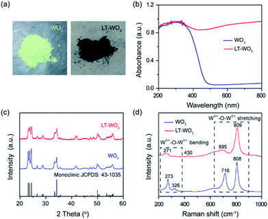
Monoclinic WO3 nanoplates were first synthesized by directly annealing tungstic acid at 550 °C, which was afforded by a simple co-precipitation of sodium tungstate solution with HCl. To introduce a disordered layer, the as-prepared WO3 nanoplates were dispersed and stirred in Li-EDA solution35 at room temperature for 4 h. During the Li-EDA treatment, a distinct color change from pale yellow to dark blue was observed (Fig. 1a). The UV-vis diffuse reflectance spectra (UV-vis DRS, Fig. 1b) reveal that the light response of Li-EDA treated WO3 (LT-WO3) has been extended, as evident from a significant absorption tail in the visible region (450 to 800 nm).Such a change in optical properties can arise from the oxygen vacancies created on the surface or modified crystal phase.36,37 X-ray diffraction (XRD) analysis was conducted to investigate the structural changes induced by Li-EDA treatment. As shown in Fig. 1c, the XRD pattern of pristine WO3 matches well with that of the monoclinic phase of WO3 (JCPDS no. 43-1035) where the sharp diffraction peaks indicate its crystalline nature. LT-WO3 also shows a similar pattern of diffraction peaks, indicating that the crystal structure is retained. However, the peaks are broader with much weaker intensities compared to those observed for pristine WO3, suggesting reduced crystallinity due to the localized modification of the crystal structure.36
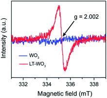
A similar change was observed in the Raman spectra (Fig. 1d), where the characteristic Raman peaks of WO3 are broadened after the Li-EDA treatment. The two peaks at 273 and 326 cm−1, which are assigned to the W6+–O–W6+ bending vibration mode of bridging oxygen in the WO3 crystal lattice,38 almost disappeared in the LT-WO3 spectrum, suggesting the partial removal of oxygen atoms. The peak at 716 cm−1 that is attributed to the long W6+–O–W6+ bond stretching mode was also markedly reduced with a slight shift. In addition, the peak for the short W6+–O–W6+ bond stretching at 808 cm−1 shows an appreciable broadening that is correlated to the weakening of the W–O bond.38 Furthermore, a small peak at 430 cm−1 appeared after the Li-EDA treatment, indicating the presence of W species at lower oxidation states.38–40 The reduction of W6+ to a lower oxidation state by Li-EDA is believed to weaken the W–O bond, which in turn leads to the partial loss of oxygen from the lattice. This is supported by the electron paramagnetic resonance (EPR) studies where only LT-WO3 shows a signal at a g-value of 2.002, an indication of oxygen vacancies (Fig. 2).14 Both Raman and EPR results are in good agreement with the observations from XRD measurements.
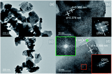
Fig. 3 compares the transmission electron microscopy (TEM) images of the as-prepared WO3 and LT-WO3 nanoplates. The typical morphology of WO3 is rectangular nanoplates (with a mean side length of ca. 130 nm) with some smaller nanoplates of irregular shapes (Fig. 3a). A high resolution TEM (HR-TEM) image shown in Fig. 3b clearly reveals well-ordered lattice fringes of 0.366 and 0.378 nm that can be indexed to the (200) and (020) planes of monoclinic phase WO3, respectively. The corresponding selected area electron diffraction (SAED) pattern (inset in Fig. 3b) shows the single-crystal spots that are in good agreement with the (200) and (020) planes. On the other hand, the TEM image of LT-WO3 (Fig. 3c) shows a similar but more round-shaped morphology with a slightly reduced average side length (ca. 77 nm). Moreover, in the HR-TEM image (Fig. 3d), a thin disordered layer (average thickness = ca. 2 nm) is evident along the edge, which is supported by the disappearance of lattice fringes and the corresponding SAED pattern (inset in Fig. 3d). The formation of the disordered layer is attributed to the removal of surface lattice oxygen by solvated electrons during the treatment with Li-EDA, which is a strong reducing agent.41 By reacting with Li-EDA, W6+ is reduced to a lower oxidation state, and oxygen atoms are removed from the surface lattice.18,35,42 The removal of oxygen atoms would lead to the crystal lattice deformation on the surface, leading to the decrease in both crystallinity and size of the nanoplates as observed from the XRD, TEM, and Raman spectroscopic studies.
It is interesting that the core part of LT-WO3 still retained the crystallinity as manifested by the clear lattice fringes (Fig. 3d). We have conducted a series of time-resolved Li-EDA treatments to investigate the formation of the disordered layer and control its thickness (Fig. 4). The disordered layer starts to form on the edges after 2 h of reaction and gradually grows thicker with treatment time. The thickness of the disordered layer reached up to 5 nm after 7 h; however, further prolonged reaction did not change the thickness, but only reduced the nanoplate size. The reaction between Li-EDA and WO3 initially occurs at the Li-EDA/WO3 interface. In the early stage, solvated electrons can diffuse through the thin disordered layer formed on the surface to reduce the W6+ ions in the inner crystal lattice. As the disordered layer becomes thicker, it acts as a passivation layer that hinders the diffusion of the electrons into the inner part. With further extended reaction time, the size of the core shrinks, as the outer layer is lost. These results suggest that the surface disordered layer is closely associated with the formation of oxygen vacancies.
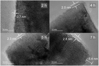 | ||
| Fig. 4 Time-resolved TEM analysis of the thickness of the disordered layer in LT-WO3 nanoplates treated for 2, 4, 5, and 7 h. | ||
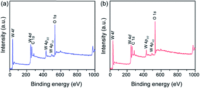
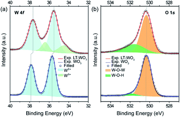
To confirm the formation of the disordered layer, the surface species was characterized using X-ray photoelectron spectroscopy (XPS). Similar survey XPS spectra were obtained from pristine WO3 and LT-WO3, where only W and O were identified, with a small C 1s peak due to the adsorbed carbon-containing species, eliminating the possibility of Li contamination (binding energy of Li 1s is ca. 55.0 eV), especially in LT-WO3 (Fig. 5). In the normalized W 4f core level spectra (Fig. 6a), only W6+ ions are detected for pristine WO3, with the peaks at binding energies of 35.7 and 37.8 eV assigned to W 4f5/2 and W 4f7/2, respectively.14 In contrast, the W 4f spectrum of LT-WO3 shifts to a lower binding energy and becomes broader, indicating the presence of lower oxidation states. In addition to the W6+ state, W5+ ions appear as a shoulder at binding energies of 34.5 and 36.4 eV. This is in good accordance with the Raman studies and further validates the reduction of W6+ to a lower oxidation state by Li-EDA. Additionally, a broad peak was seen in the O 1s spectrum of LT-WO3 (Fig. 6b), which can be deconvoluted into two peaks. The peak centered at 530.4 eV is ascribed to the lattice O2− species (W–O–W),14 while the other peak centered at 531.6 eV is assigned to O2− in the vicinity of oxygen vacancies.43 Meanwhile, the O 1s spectrum of pristine WO3 shows a major peak for lattice oxygen atoms at 530.3 eV with a small peak at 531.6 eV, presumably due to the surface contamination during sample preparation. It is noted that both W 4f and O 1s peaks of LT-WO3 exhibit binding energies slightly shifted to the lower values, ca. 0.2 and 0.1 eV, respectively. Similar shifts were observed for WO3 after the chemical treatment as a result of the change in the electronic structure.26,44
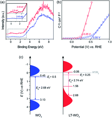
A disordered atomic arrangement is known to affect the electronic structure, and thus the physicochemical properties of WO3.16,25,26 The observed change in the optical absorption of LT-WO3 is related to the surface disordered layer. The band gap energies calculated by fitting the UV-vis DRS to the Tauc equation are 2.68 and 2.74 eV for WO3 and LT-WO3, respectively (Fig. S1†). Despite the obvious color change, the optical band gap energies (Eg) did not show much difference. However, the valence band XPS (VB-XPS) spectra reveal the changes in the electronic structure and band offset (Fig. 7a). The position of the VB maximum (VBM) was first evaluated by linearly extrapolating the onset of XPS valence band spectra to the baseline, which reflects a band edge position with respect to the Fermi level (Ef). The VBM edge levels of WO3 and LT-WO3 were determined to be 2.63 and 2.43 eV, respectively, indicating the upshift of the VBM by the induced oxygen vacancies. Interestingly, the VB-XPS spectrum of LT-WO3 also exhibits the VB tail state (1.31 eV with respect to Ef), suggesting the formation of an additional electronic state. This mid-gap state would essentially broaden the VB width to create a reduced band gap  and consequently allows the wider visible light absorption and change in sample color to dark blue.45 We also used the Mott–Schottky plots to determine the Ef levels and thus obtain the band structures of samples.46,47Fig. 7b shows the flat band potentials, which shifted from 0.5 to 0.25 V after Li-EDA treatment. The flat band potential reflects the difference between the Ef level and the water reduction potential of the sample. This shift of Ef confirms again that the surface disordered layer reconstructs the electronic structure of WO3 by introducing oxygen vacancies. The formation of the mid-gap is closely related to the disordered surface layer on LT-WO3, which contains W5+ ions and oxygen vacancies (Fig. 6). The self-doping of W5+ ions also modifies the electronic structure by creating a mid-gap and enhances the surface electron density, contributing to the upshift of the Ef.16,48,49
Combining the results from UV-vis DRS, VB-XPS, and Mott–Schottky plots, we have constructed an energy level diagram qualitatively representing the changes in the band structure of LT-WO3, and presented in Fig. 7c. The conduction band minimum (CBM) was estimated according to the equation ECBM = EVBM − Eg. The upshift of the Ef induced by the disordered layer on LT-WO3 caused the VBM shift from 3.13 to 2.68 V. With an Eg of 2.74 eV, the CBM in LT-WO3 is determined to be −0.06 V, which satisfies the thermodynamic requirement for H2 generation.
To verify this reformed band structure of LT-WO3, we have carried out the photocatalytic HER using a mixed solution of Na2S and Na2SO3 as a sacrificial agent under one sun illumination. LT-WO3 indeed shows a remarkable performance in the photocatalytic HER with an average rate of 94.2 μmol g−1 h−1 (Fig. 8). The H2 generation rate was stable during the continuous 25 h reaction, showing no discernable degradation in the catalytic activity. The control experiment conducted in the dark generated no detectable H2. To the best of our knowledge, this is the first report of photocatalytic H2 evolution using WO3 without any co-catalysts. The creation of a disordered surface layer on WO3 is demonstrated to modify its electronic structure, thus endowing it with a new capability of photocatalytic H2 generation. It also seems to affect the generation and lifetime of charge carriers. The steady state photoluminescence (PL) spectra (Fig. S2a†) recorded at room temperature show a much enhanced PL emission intensity, attributed to the higher concentration of photogenerated excitons. The time-resolved PL spectra (Fig. S2b†) indicate that the charge carriers in LT-WO3 have more than 4 times longer lifetime (1.05 ± 0.05 ns) than those in WO3 (0.25 ± 0.05 ns).
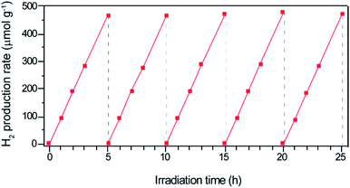 | ||
| Fig. 8 Photocatalytic H2 production using LT-WO3 as a photocatalyst for 25 h reaction of five cycles. | ||
In order to gain further insight on the disordered surface layer of LT-WO3, the surface reactivity was studied by examining the electrocatalytic activity in H2 production. Fig. 9a shows the polarization curves where the normalized current densities are plotted against applied potential without iR correction. LT-WO3 shows a much lower overpotential (η) of −176 mV (vs. RHE, the same below) at a current density of 10 mA cm−2 compared with that of pristine WO3 (−667 mV). The corresponding Tafel slope of LT-WO3 is 59 mV dec−1 (Fig. 9b), lower than that of WO3 (88 mV dec−1), implying its higher activities towards H2 production. These results indicate that the disordered layer on the WO3 surface can significantly improve the surface reactivity towards H2 production. The increased population of trapping sites for electron carriers (i.e., oxygen vacancies) is believed to promote the electron transfer, which effectively reduces the energy barrier for proton reduction, and activates the surface reactivity towards H2 production.26,27
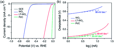 | ||
| Fig. 9 (a) Polarization curves and (b) Tafel plots of WO3 and LT-WO3, with Pt/C electrodes included for comparison. | ||
Conclusions
In conclusion, the band structure of WO3 has been successfully tuned by a simple surface defect engineering method, Li-EDA treatment. The formation of oxygen vacancies and self-doping of W5+ onto the surface of WO3 through the generation of a disordered surface layer create a mid-gap level in the electronic structure and shift the CBM above the H2 reduction potential. This is the first example of tuning the band structure of WO3 to realize co-catalyst-free photocatalytic H2 evolution. Electrochemical investigations also reveal that the oxygen vacancy-rich disordered layer can provide efficient electron trapping sites that promote the surface activity for the HER. Our work demonstrates that a disordered layer on a semiconductor surface can be utilized to effectively tune the band structure and extend its catalytic applications.Conflicts of interest
There are no conflicts to declare.Acknowledgements
This work was supported by the Innovation and Technology Commission, The Hong Kong Polytechnic University (Grant No. G-YBSZ and 1-BE0Y), and the National Natural Science Foundation of China (Grants No. 21701135). L. W. acknowledges the award of a postdoctoral fellowship by The Hong Kong Polytechnic University. K. Y. W. acknowledges the support by the Patrick S. C. Poon endowed professorship.Notes and references
- T. Hisatomi, J. Kubota and K. Domen, Chem. Soc. Rev., 2014, 43, 7520–7535 RSC.
- J. H. Montoya, L. C. Seitz, P. Chakthranont, A. Vojvodic, T. F. Jaramillo and J. K. Nørskov, Nat. Mater., 2016, 16, 70 CrossRef.
- Y. Wang, H. Suzuki, J. Xie, O. Tomita, D. J. Martin, M. Higashi, D. Kong, R. Abe and J. Tang, Chem. Rev., 2018, 118, 5201–5241 CrossRef CAS.
- S. Fukuzumi, Y.-M. Lee and W. Nam, Coord. Chem. Rev., 2018, 355, 54–73 CrossRef CAS.
- E. Ha, L. Y. S. Lee, J. Wang, F. Li, K.-Y. Wong and S. C. E. Tsang, Adv. Mater., 2014, 26, 3496–3500 CrossRef CAS.
- J. Zhang, W. Yao, C. Huang, P. Shi and Q. Xu, J. Mater. Chem. A, 2017, 5, 12513–12519 RSC.
- W. Liu, E. Ha, L. Wang, L. Hu, L. Y. S. Lee and K.-Y. Wong, Adv. Mater. Interfaces, 2018, 5, 1800611 CrossRef.
- I. Concina, Z. H. Ibupoto and A. Vomiero, Adv. Energy Mater., 2017, 7, 1700706 CrossRef.
- G. Wang, Y. Yang, D. Han and Y. Li, Nano Today, 2017, 13, 23–39 CrossRef CAS.
- P. Kofstad, Phase Transitions, 1996, 58, 75–93 CrossRef CAS.
- J. Nowotny, M. A. Alim, T. Bak, M. A. Idris, M. Ionescu, K. Prince, M. Z. Sahdan, K. Sopian, M. A. Mat Teridi and W. Sigmund, Chem. Soc. Rev., 2015, 44, 8424–8442 RSC.
- J. Jia, C. Qian, Y. Dong, Y. F. Li, H. Wang, M. Ghoussoub, K. T. Butler, A. Walsh and G. A. Ozin, Chem. Soc. Rev., 2017, 46, 4631–4644 RSC.
- X. Pan, M.-Q. Yang, X. Fu, N. Zhang and Y.-J. Xu, Nanoscale, 2013, 5, 3601–3614 RSC.
- J. Meng, Q. Lin, T. Chen, X. Wei, J. Li and Z. Zhang, Nanoscale, 2018, 10, 2908–2915 RSC.
- Y. Yang, Y. Wang and S. Yin, Appl. Surf. Sci., 2017, 420, 399–406 CrossRef CAS.
- X. Chen, L. Liu, P. Y. Yu and S. S. Mao, Science, 2011, 331, 746–750 CrossRef CAS.
- Y. Liu, Y. Li, S. Yang, Y. Lin, J. Zuo, H. Liang and F. Peng, ChemSusChem, 2018, 11, 2766 CrossRef CAS.
- G. Yin, X. Huang, T. Chen, W. Zhao, Q. Bi, J. Xu, Y. Han and F. Huang, ACS Catal., 2018, 8, 1009–1017 CrossRef CAS.
- P. Yan, G. Liu, C. Ding, H. Han, J. Shi, Y. Gan and C. Li, ACS Appl. Mater. Interfaces, 2015, 7, 3791–3796 CrossRef CAS.
- G. Wang, H. Wang, Y. Ling, Y. Tang, X. Yang, R. C. Fitzmorris, C. Wang, J. Z. Zhang and Y. Li, Nano Lett., 2011, 11, 3026–3033 CrossRef CAS.
- S. W. Kwon, M. Ma, M. J. Jeong, K. Zhang, S. J. Kim and J. H. Park, Chem. Commun., 2016, 52, 13807–13810 RSC.
- Y. Cho, S. Kim, B. Park, C. L. Lee, J. K. Kim, K. S. Lee, I. Y. Choi, J. K. Kim, K. Zhang, S. H. Oh and J. H. Park, Nano Lett., 2018, 18, 4257–4262 CrossRef CAS.
- S. Sun, T. Zhai, C. Liang, S. V. Savilov and H. Xia, Nano Energy, 2018, 45, 390–397 CrossRef CAS.
- T. Xia, P. Wallenmeyer, A. Anderson, J. Murowchick, L. Liu and X. Chen, RSC Adv., 2014, 4, 41654–41658 RSC.
- K. J. Kyu, C. Yoonjun, J. M. Jin, L.-W. Ben, S. Dongguen, Y. Yeonjin, W. D. Hwan, Z. Xiaolin and P. J. Hyeok, ChemSusChem, 2018, 11, 933–940 CrossRef.
- M. Ma, K. Zhang, P. Li, M. S. Jung, M. J. Jeong and J. H. Park, Angew. Chem., Int. Ed., 2016, 55, 11819–11823 CrossRef CAS.
- R. Zhang, F. Ning, S. Xu, L. Zhou, M. Shao and M. Wei, Electrochim. Acta, 2018, 274, 217–223 CrossRef CAS.
- H. Zheng, Y. Tachibana and K. Kalantar-zadeh, Langmuir, 2010, 26, 19148–19152 CrossRef CAS.
- S.-H. Lee, R. Deshpande, P. A. Parilla, K. M. Jones, B. To, A. H. Mahan and A. C. Dillon, Adv. Mater., 2006, 18, 763–766 CrossRef CAS.
- R. Xing, Y. Du, X. Zhao and X. Zhang, Sensors, 2017, 17, 710 CrossRef.
- X. Shi, I. Y. Choi, K. Zhang, J. Kwon, D. Y. Kim, J. K. Lee, S. H. Oh, J. K. Kim and J. H. Park, Nat. Commun., 2014, 5, 4775 CrossRef CAS.
- H. Zhen-Feng, S. Jiajia, P. Lun, Z. Xiangwen, W. Li and Z. Ji-Jun, Adv. Mater., 2015, 27, 5309–5327 CrossRef.
- C. A. Bignozzi, S. Caramori, V. Cristino, R. Argazzi, L. Meda and A. Tacca, Chem. Soc. Rev., 2013, 42, 2228–2246 RSC.
- Y. H. Li, P. F. Liu, L. F. Pan, H. F. Wang, Z. Z. Yang, L. R. Zheng, P. Hu, H. J. Zhao, L. Gu and H. G. Yang, Nat. Commun., 2015, 6, 8064 CrossRef CAS.
- K. Zhang, L. Wang, J. K. Kim, M. Ma, G. Veerappan, C.-L. Lee, K.-j. Kong, H. Lee and J. H. Park, Energy Environ. Sci., 2016, 9, 499–503 RSC.
- G. Wang, Y. Ling, H. Wang, X. Yang, C. Wang, J. Z. Zhang and Y. Li, Energy Environ. Sci., 2012, 5, 6180–6187 RSC.
- J. Song, Z.-F. Huang, L. Pan, J.-J. Zou, X. Zhang and L. Wang, ACS Catal., 2015, 5, 6594–6599 CrossRef CAS.
- S. Bai, K. Zhang, L. Wang, J. Sun, R. Luo, D. Li and A. Chen, J. Mater. Chem. A, 2014, 2, 7927–7934 RSC.
- S.-H. Lee, H. M. Cheong, J.-G. Zhang, A. Mascarenhas, D. K. Benson and S. K. Deb, Appl. Phys. Lett., 1999, 74, 242–244 CrossRef CAS.
- W. Chun-Kai, D. R. Sahu, W. Sheng-Chang, L. Chung-Kwei and H. Jow-Lay, J. Phys. D: Appl. Phys., 2012, 45, 225303 CrossRef.
- R. S. Monson, in Advanced Organic Synthesis, ed. R. S. Monson, Academic Press, 1971, pp. 25–30, DOI:10.1016/B978-0-12-504950-4.50006-X.
- M. Ming, Z. Kan, L. Ping, J. M. Sun, J. M. Jin and P. J. Hyeok, Angew. Chem., Int. Ed., 2016, 55, 11819–11823 CrossRef.
- Y. Sun, W. Wang, J. Qin, D. Zhao, B. Mao, Y. Xiao and M. Cao, Electrochim. Acta, 2016, 187, 329–339 CrossRef CAS.
- H. Cheng, M. Klapproth, A. Sagaltchik, S. Li and A. Thomas, J. Mater. Chem. A, 2018, 6, 2249–2256 RSC.
- J. Liu, L. Han, N. An, L. Xing, H. Ma, L. Cheng, J. Yang and Q. Zhang, Appl. Catal., B, 2017, 202, 642–652 CrossRef CAS.
- J. Liu, J. Ke, D. Li, H. Sun, P. Liang, X. Duan, W. Tian, M. O. Tadé, S. Liu and S. Wang, ACS Appl. Mater. Interfaces, 2017, 9, 11678–11688 CrossRef CAS.
- L. Liao, Q. Zhang, Z. Su, Z. Zhao, Y. Wang, Y. Li, X. Lu, D. Wei, G. Feng, Q. Yu, X. Cai, J. Zhao, Z. Ren, H. Fang, F. Robles-Hernandez, S. Baldelli and J. Bao, Nat. Nanotechnol., 2013, 9, 69 CrossRef.
- F. Zuo, L. Wang, T. Wu, Z. Zhang, D. Borchardt and P. Feng, J. Am. Chem. Soc., 2010, 132, 11856–11857 CrossRef CAS PubMed.
- W. Huang, J. Wang, L. Bian, C. Zhao, D. Liu, C. Guo, B. Yang and W. Cao, Phys. Chem. Chem. Phys., 2018, 20, 17268–17278 RSC.
Footnote |
| † Electronic supplementary information (ESI) available. See DOI: 10.1039/c8ta09446b |
| This journal is © The Royal Society of Chemistry 2019 |

