 Open Access Article
Nucleation density and pore size tunable growth of ZnO nanowalls by a facile solution approach: growth mechanism and NO2 gas sensing properties†
Chun Li ab,
Lingmin Yu*a,
Xinhui Fan*ab,
Mingli Yina,
Ning Nana,
Le Cuia,
Shuai Maa,
Yuan Lia and
Bo Zhanga
aSchool of Materials and Chemical Engineering, Xi'an Technological University, Xi'an 710021, P. R. China. E-mail: ylmyl@163.com; fxh_slxy@163.com
bShaanxi Key Laboratory of Comprehensive Utilization of Tailings Resources, Shangluo University, Shangluo 72600, China
First published on 20th January 2020
Abstract
Nanowalls are novel nanostructures whose 3D porous network morphology holds great potential for applications as gas sensors. The realization of such a nanowall-based gas sensor depends directly on the comprehensive understanding of the growth mechanism of the nanowalls. We induced nucleation density and pore size evolution by increasing the dipping and growth times. The investigation indicates that the 3D porous ZnO nanowalls consist of a seed layer of ZnO nanoparticles and a growth layer of the vertically grown ZnO nanosheets. The seed layer nucleation density dominance is driven by the dipping time. The pore size and the height of the as-grown ZnO nanowalls are determined by varying the growth time. Possible growth mechanisms governing the physical characteristics of the synthesized ZnO nanostructures in the solution process are proposed and discussed. The gas sensor that was fabricated from the ZnO nanowall structure exhibited strong dependence on the microstructure, which was mainly determined by the preparation conditions.
1 Introduction
The ever-increasing human health protection and air quality monitoring demands have become some of the key issues that have led to the development of gas sensing technologies for efficient gas detection.1–7 The surface reaction kinetics between the physisorbed oxygen species and the target gas molecules involved in these gas sensing systems are one of the key points to be tackled.8–10 It is well-known that these reactions usually involve a complicated multi-electron transfer process, which is limited greatly by the electron transportation channels and active sites. To address these problems, the design and control of novel materials with a tuned structure and high performance are thus crucial for fundamental studies and applications as the building blocks of gas sensors. In the continual research efforts for the miniaturization of gas sensors, quasi two-dimensional (2D) ZnO nanowalls have been proven to be potential candidates due to their unique properties such as the 2D layers of atomic planes grown perpendicular to the substrate, a huge surface-to-volume ratio supplying numerous active sites for gas adsorption, and numerous hierarchical porous structures and channels for electron transportation, thus further leading to enhanced gas properties.11–15In recent years, the synthesis of ZnO nanowalls by a solution-based process has become the focus of researchers due to its low temperature and cost, which is especially suitable for large-area production.16–19 Nevertheless, the perfect control of the ZnO nanowall nucleation, density, aspect ratio, and alignment with controlled gas sensing properties still needs to be tuned precisely and conveniently to ensure that the gas molecules can get access to the surface and pores in the ZnO nanowalls with tuned thickness. Moreover, it is still a major challenge to comprehensively understand the ZnO nanowall growth mechanisms and the corresponding gas sensing mechanisms.
In this study, we report a simple strategy for the in situ assembly of ZnO nanowalls with enriched surface-active sites by employing a two-stage solution method. Material analysis was conducted to clarify the effect of the dipping time in the first growth stage and the growth time in the second growth stage on the morphologies of the ZnO nanowalls. The growth mechanism was found to cause variations in nucleation density, nanowall height, and nanopore size, which locally affected the gas sensing properties of the nanowalls.
2 Results and discussion
2.1 Growth process of ZnO nanowalls
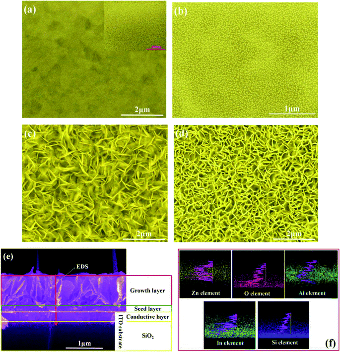
Fig. 1 shows the SEM images of the ZnO nanowalls prepared by the solution method on the ITO glass substrate at different steps. Fig. 1(a) presents a surface view of the precursor on the ITO substrate in Step 1. A more continuous network of the uniformly distributed precursor on the ITO substrate is clearly visible in the high-magnification image provided as an inset in Fig. 1(a). After the annealing treatment (Step 2), the continuous network structure evolved into granular grains (see Fig. 1(b)), and the average grain size was about 13 nm. These granular grains were fundamental for obtaining the ZnO nanowall structure. The as-prepared ZnO film, grown using aqueous Zn(NO3)2·6H2O and (CH2)6N4 at 80 °C (Step 3), exhibited a 3D porous structure composed of cross-linked porous walls with a thickness of ∼18 nm (see Fig. 1(c)). However, the nanowalls and pores were not distributed uniformly. After the annealing treatment at 450 °C for 1 h (Step 4), the large-scale and high-density 3D ZnO nanowalls were uniformly distributed on the ITO glass substrate surface (see Fig. 1(d)).From the cross-sectional FE-SEM images shown in Fig. 1(e), we can observe that the ZnO nanowall film consists of two layers: (i) a seed layer composed of ZnO nanoparticles with a thickness of 155 nm and (ii) a growth layer composed of vertically grown ZnO nanosheets with a height of 743 nm. The side elemental distribution along the growth direction, shown as a defined red line in Fig. 1(e), was analyzed by the EDS technique and the results are shown in Fig. 1(f). It can be seen from Fig. 1(f) that zinc and oxygen are homogeneously distributed in the ZnO film and indium and silicon are from the ITO glass substrate. Aluminum was mainly concentrated in the seed layer and a few Al species diffused into the growth layer. Yu20 et al. believed that Al3+ plays a critical role in synthesizing the ZnO nanowalls, and ZnAl2O4 may support easy nucleation for ZnO due to the reduced surface energy of the ITO glass substrate. The binding of Al(OH)4− to Zn2+ in the seed layer surface played a critical role in blocking the ZnO growth along the c-axis direction and promoting the lateral growth.21,22
TEM was used to further clarify the morphology and crystal structure of the ZnO nanowalls. It can be seen from the TEM images (see Fig. S1(a)†) that the ZnO nanowalls appear to be a single layer that is very smooth. As shown in Fig. S1(b)† (HR-TEM image), a well-ordered crystal lattice array without defects is observed. The lattice spacing between the adjacent planes was about 0.28 nm, which corresponded to the interplanar spacing of ZnO (0002). It was further confirmed that the ZnO nanowalls grew preferentially along the [0001] direction.
Fig. S2 in the ESI† shows the XRD patterns of the ZnO nanowalls at (a) Step 1, (b) Step 2, (c) Step 3, and (d) Step 4. In Fig. S2(a),† two diffractive peaks (2θ = 9.8° and 19.4°) probably originating from Zn5(OH)8(Ac)2·2H2O and Zn5(OH)8(NO3)2·2H2O, respectively, can be observed. Zn5(OH)8(Ac)2·2H2O and Zn5(OH)8(NO3)2·2H2O belong to Zn-based hydroxide double salts (so-called Zn-HDS). Tokumoto23 et al. thought that the layered Zn-HDS structures presented a characteristic peak at a low angle (2θ < 10°) due to the (001) reflection, corresponding to the interlayer distances. A small peak (21.4°) for the Al(OH)3 phase was also observed. Fig. S2(b)† shows that the diffraction peaks at 31.88°, 34.54°, and 36.38° can be indexed to the (100), (002) and (101) planes, respectively, of ZnO with a hexagonal phase (PDF#36-1451). Meanwhile, the peak (21.4°) of the Al(OH)3 phase was also observed. Fig. S2(c) and (d)† show the XRD patterns of the hydrothermal growth (Step 3) and annealing treatment (Step 4) of the ZnO nanowalls, respectively. The samples obtained at different stages also revealed diffraction peaks for the ZnO phase, which were around 31.88°, 34.54°, 36.38°, 47.64°, 56.62°and 63.06°.
To further determine the nature of the precursor, FT-IR transmittance spectra of the films were recorded (Fig. S3(a)†). The bands at about 1568 and 1376 cm−1 were from the –COO– group. The weak band at 1043 cm−1 was attributed to the N–O stretching of the free nitrate group, and the nitrate absorption band was the weak band at 832 cm−1.24 The band at 683 cm−1 was due to the vibrational absorption of the hydroxyl (–OH–) group from Zn(OH)2. Combined with ref. 25 and 26, the bands at about 1568 and 1376 cm−1 belonged to the absorption bands of Zn5(OH)8(Ac)2·2H2O. Meanwhile, Zn5(OH)8(NO3)2·2H2O was formed by an exchange between the Ac− and NO3− ions. Compared with the observations reported by Lee26 et al. where the peaks at 1551 and 1344 cm−1 corresponded to Zn5(OH)8(Ac)2·2H2O, in this work, the red shift in the peaks at 1568 and 1376 cm−1 was probably due to Zn5(OH)8(NO3)2·2H2O. Hence, we could determine that the main phase of the precursor was Zn-HDS (including Zn5(OH)8(Ac)2·2H2O + Zn5(OH)8(NO3)2·2H2O) in Step 1. After the annealing treatment (see Fig. S3(b)†), the bands at 1568, 1376, and 1043 cm−1 weakened or disappeared due to the decomposition of Zn-HDS. ZnO was generated, and this was indicated by the much stronger Zn–O band at 490 cm−1.
2.2 Effect of the dipping times on nucleation density
The morphology of the ZnO nanowalls was easily controlled by varying the dipping times or the density of the ZnO nucleus on the ITO substrate. As a result, we successfully controlled the ZnO nanowall morphology by manipulating the ZnO nucleus density, as shown in Fig. 2. The FE-SEM images in Fig. 2(a)–(c) and 1(b) show that as the dipping times increase from 2 to 8 times, the density of the ZnO nucleus also increases. When the dipping times increased to 8, the ZnO nucleation in the seed layer evolved into a semi-continuous network structure (see Fig. 2(c)). Meanwhile, from the FE-SEM images in Fig. 2(e), (f) and 1(d), we can infer that the number of ZnO nanowalls increases and the size of the pores, which are surrounded by the ZnO nanowalls, decreases and they are distributed uniformly.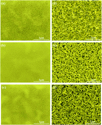 | ||
| Fig. 2 ZnO nucleation at different dipping times: (a) 2, (b) 6, and (c) 8. Tilted-view FE-SEM images of the ZnO nanowalls at different dipping times: (d) 2, (e) 6, and (f) 8. | ||
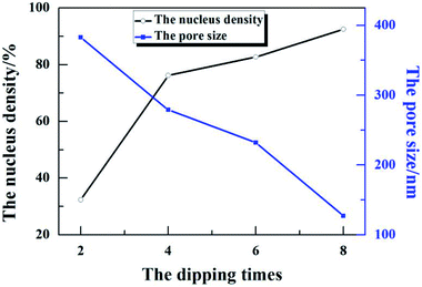
According to the surface morphology of the ZnO nanostructures shown in Fig. 2, 1(b) and (d), the density of the ZnO nucleus and pore size were measured by Image-Pro Plus 6.0, as shown in Fig. 3. After dipping for 2 times, the density of the ZnO nucleus was ∼32% and the pore size was ∼383 nm. After further increasing the dipping times to 4–6, the density was 76–82% (see Fig. 2(b) and 7(b)) and the pore size was 279–232 nm. With the further increase in the dipping times to 8, the density of the ZnO nucleus continued to increase to 92% (see Fig. 2(c)) and the ZnO nanowalls could fill the air gap and even stack together, leading to a decrease in the pore size to 127 nm. As the dipping times increased, additional nucleation was observed, which provided more growth sites for the ZnO nanowalls and led to a decrease in the 3D pore size (see Fig. 3). This study suggests that the dipping times play an important role in the formation of the ZnO nanowalls.
Fig. S4† shows the X-ray diffraction (XRD) patterns of the ZnO nanowalls at different dipping times. It could be seen that all samples showed characteristic peaks of the ZnO phase. The diffraction peaks corresponding to the (100), (002), and (004) planes indicated that the nanowall structure grew vertically along the c-axis. However, after dipping 4 times, it was very difficult to observe the diffraction peaks related to the (004) plane. When the dipping times increased to 8, the diffraction peaks for the (002), (101), (102), and (103) planes were barely observed. The increase in the nucleus supplied more growth sites for the ZnO nanowalls, which lead to grow incompletely for some planes due to the competition in the growth.
2.3 Effect of the growth time on the pore size of ZnO nanowalls
Different ZnO nanowall morphologies were obtained by controlling the growth time, as shown in Fig. 4. The tilted-view FE-SEM images in Fig. 4(a)–(e) show the morphologies of the vertically aligned ZnO nanowalls on the ITO substrates grown with different growth times of 1 h, 2 h, 3 h, 4 h and 8 h at 80 °C. It could be seen that on increasing the growth time, the numbers of nanowalls increased and the size of the pores, which were surrounded by the nanowalls, decreased. From the cross-sectional FE-SEM images shown in Fig. 4(f)–(j), the height of the ZnO nanowalls was estimated. The isolated nanowalls started to grow along the c-axis and evolved into a nanowall structure on increasing the growth time.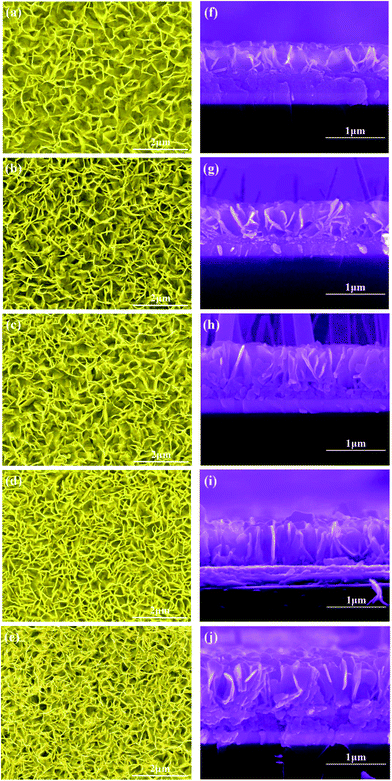 | ||
| Fig. 4 Tilted-view and cross-sectional FE-SEM images of the ZnO nanowalls at different growth times: (a) and (f) 1 h, (b) and (g) 2 h, (c) and (h) 3 h, (d) and (i) 4 h, (e) and (j) 8 h. | ||
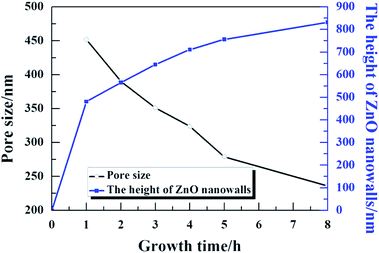
Fig. 5 presents the pore size and height of the ZnO nanowalls at different growth times. The pore size of the nanowalls decreased on increasing the growth time (see the black line); the blue line indicates the height of the ZnO nanowalls. Within one hour, the ZnO nanowalls grew quickly (∼8 nm min−1), and the size of the nanowalls increased from 0 to 481 nm. On increasing the growth time, the growth rate slowed down. However, the ZnO nanowalls maintained a linear growth rate of about 1.37 nm min−1 and within 3 h, nanowalls of about 645 nm height were realized. After 3 h, a gradual decrease in the growth rate of the nanowalls was observed. Furthermore, with an increase in the growth time to 5 h and 8 h, the heights of the ZnO nanowalls increased to about 711 nm and 756 nm, respectively. Hence, the synthesis of solution-grown ZnO nanowalls included 3 stages: (i) a quick growth stage, (ii) a slow growth stage, and (iii) an exponential decay growth stage.
Fig. S5† shows the X-ray diffraction (XRD) patterns of the ZnO nanowalls at different growth times. The diffraction peak related to the (100) plane indicated that the nanowalls grew vertically and oriented along the c-axis in all the samples. When the growth time was below 3 h, only the diffraction peak of the (100) plane was observed. This indicated that the ZnO phase of the (100) plane grew first during the solution synthesis of the ZnO nanowalls. After 4 h, the diffraction peaks related to the (002), (101), and (103) planes were observed. When the growth time reached 5 h, the diffraction peaks related to the (102) and (110) planes were found. With the increase in the growth time, the height of the ZnO nanowalls increased, resulting in the extrusion of some of them. Kim27 et al. also observed that the (101), (102), and (103) planes were from the bent nanowalls.
2.4 Growth mechanism of ZnO nanowalls
The above-mentioned results provide detailed features of the growth process of the ZnO nanowalls. The growth mechanism of the 3D ZnO nanowalls prepared by the solution method is shown in Fig. 6. First, the precursors were used as the reaction products of Zn(CH3COO)2·2H2O and Al(NO3)3·9H2O in absolute alcohol. The experimental results (see Fig. S2 and S3†) confirmed that the acetate derivative zinc hydroxide double salt Zn5(OH)8(Ac)2·2H2O was formed in Step 1. Meanwhile, due to the NO3− ions being supplied by Al(NO3)3·9H2O, Zn5(OH)8(NO3)2·2H2O was formed. Grasset28 et al. reported that Zn5(OH)8(Ac)2·2H2O and Zn5(OH)8(NO3)2·2H2O belonged to the same layered materials of Zn-HDS. Hence, we could determine that the precursor of the main phase was Zn-HDS (including Zn5(OH)8(Ac)2·2H2O and Zn5(OH)8(NO3)2·2H2O) in Step 1. Zn-HDS was then coated on the substrate by the dip coating process. Meanwhile, a small amount of Al(OH)3 was also introduced in the film. The detailed chemical reactions are as follows (eqn (1)–(4)):| Zn(Ac)2·2H2O → Zn2+ + 2Ac− + 2H2O | (1) |
| Al(NO3)3·9H2O → Al3+ + 3NO3− + 9H2O | (2) |
| 10Zn2+ + 10Ac− + 22H2O + 10NO3− → Zn5(OH)8(Ac)2·2H2O + Zn5(OH)8(NO3)2·2H2O + 8HAc + 8HNO3 | (3) |
| Al3+ + 3OH− → Al(OH)3 | (4) |
 | ||
| Fig. 6 Schematic of the growth mechanism of the hydrothermally synthesized 3D ZnO nanowalls on the ITO substrate. | ||
Second, a large quantity of spherical ZnO nanoparticles was generated from the decomposition of Zn-HDS during the annealing treatment in Step 2. As Zn-HDS increased due to the increase in the dipping times, the number of ZnO nanoparticles also increased. The ZnO nanoparticles acted as nucleation sites for the growing nanowalls. Al(OH)3 did not change and was evenly distributed between the ZnO nanoparticles. Zn-HDS could be considered as an important intermediate product and transformed to ZnO, as presented by the following reactions (eqn (5) and (6)):
| Zn5(OH)8(Ac)2·2H2O → 2HAc + 5ZnO + 5H2O | (5) |
| Zn5(OH)8(NO3)2·2H2O → 2HNO3 + 5ZnO + 5H2O | (6) |
In the next step, the ZnO molecule obtained by the reaction of Zn (NO3)2·6H2O and (CH2)6N4 at 80 °C was supplied. Molefe29 et al. demonstrated that the growth temperature played an important role in the formation of a hexagonal wurtzite ZnO crystal structure. Pristine ZnO was formed at a temperature of 80 °C. Yu30 et al. believed that ZnO was formed by the decomposition of Zn(OH)2. The reaction temperature was continuously controlled at 80 °C for 5 h during the solution growth. We found that not only Zn(OH)2 was produced, but also part of Zn(OH)2 was decomposed into ZnO. Meanwhile, a growth competition existed between ZnO and Zn(OH)2. Compared with Zn(OH)2, ZnO in the solution had a better coherent relationship with the seed layer of ZnO. Thus, ZnO in the solution was continuously deposited on the substrate along a specific direction, resulting in the formation of the ZnO nanowalls. Another precipitated Zn(OH)2 remained in the solution (see Fig. S6†). Meanwhile, Al(OH)4− first promoted ZnO accumulation along the lateral side, resulting in the formation of the ZnO nanosheets. The detailed chemical reactions during Step 3 and 4 are as follows (eqn (7)–(10)):
| Zn(NO3)2·6H2O → Zn2+ + 3NO3− + 6H2O | (7) |
| (CH2)6N4 + 10H2O → 6HCHO + 4NH4+ + 4OH− | (8) |
| Zn2+ + 2OH− → Zn(OH)2 → ZnO + H2O | (9) |
| Al(OH)3 + OH− → Al(OH)4− | (10) |
With the increase in growth time, due to the continuous supply, the ZnO molecules accumulated on the top of the ZnO nanosheets, leading to an increase in the height of the ZnO nanowalls, and the metal pieces were connected to each other from the 3D porous ZnO nanowalls (Step 4).
3 Gas sensing performance and mechanism of ZnO nanowalls
3.1 Gas sensing performance of ZnO nanowalls
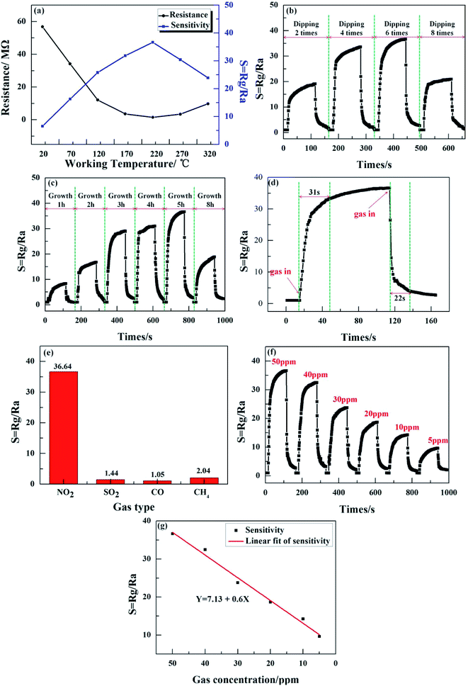
We demonstrated NO2 gas sensing as a potential application of the ZnO nanowalls; the results are shown in Fig. 7. Fig. 7(a) shows the sensitivity and resistance of the ZnO nanowalls to 50 ppm NO2 gas tested at different working temperatures. The ZnO nanowalls exhibited excellent NO2 sensing performance with the lowest resistance of 1.53 MΩ and the highest sensitivity of 36.64 at the working temperature of 220 °C.Fig. 7(b) and (c) show the sensitivity to 50 ppm NO2 gas of the 3D porous ZnO nanowalls at different dipping times and growth times, respectively. It can be seen from Fig. 7(b) and (c) that with the increase in the dipping times and growth times, the gas sensitivity increases first and then decreases. When dipped for 2 times or when the growth time was below 2 h, the gas sensitivity was lower due to the smaller numbers and lower heights of the ZnO nanowalls (see Fig. 2(d), 4(a) and (f) and 4(b) and (g)), thereby decreasing the sites of the reaction of NO2 gas with the ZnO nanowalls. When the dipping times reached 8 or the growth time reached 8 h, the sensitivity decreased because of the decrease in the 3D pore size (see Fig. 2(f) and 4(e)), thereby blocking the reaction of the NO2 gas with the ZnO nanowalls. Furthermore, when the dipping times were between 4 and 6 (see Fig. 1(d) and 4(e)) and the growth time was between 3 and 5 h (see Fig. 4(c), (d) and 1(d)), the morphology of the ZnO nanowalls was beneficial for the adsorption and desorption of NO2 gas on the surface of the ZnO nanowalls. When the dipping time was 6 or the growth time was 5 h, the highest sensitivity was 36.46.
The response/recovery times are important parameters that reflect the gas adsorption/desorption processes. The response and recovery times were 31 s and 22 s, respectively (see Fig. 7(d)). In order to examine the selectivity of the sensor, Fig. 7(e) illustrates the response of the ZnO nanowalls to various testing gases at 220 °C, including NO2, SO2, CO, and CH4, with a gas concentration of 50 ppm. These results suggested that the sensor exhibited excellent selectivity to NO2. In addition, the effect of different concentrations of NO2 (5–50 ppm) at 220 °C on the response of the sensor was investigated (see Fig. 7(e)). The responses of the sensor were 36.64, 32.48, 23.78, 18.67, 14.26, and 9.63, corresponding to 50, 40, 30, 20, 10, and 5 ppm. This proved that on increasing the gas concentration, the response value increased due to the increase in the number of NO2 molecules that reacted with the ZnO nanowalls in a short time. Fig. 7(f) shows the linear relationship of sensitivity versus the NO2 gas concentration after the linear fit. The fitting equation was Y = 7.13 + 0.6X (Y is the sensitivity and X is the NO2 gas concentration). It could be seen that the sensitivity of the sensor prepared by the ZnO nanowalls had a better linear relationship with the NO2 gas concentration. The above-mentioned results proved that the ZnO nanowalls have good potential applications in monitoring NO2 gas.
The NO2 gas sensing properties of pure ZnO with different morphological nanostructures are summarized in Table 1, as given in ref. 19, 20 and 31–36. Compared with the observations reported in ref. 19 and 20, when the dipping times increased to 6, the density of the ZnO nanowalls increased. From the comparison, the NO2 gas sensor of the ZnO nanowalls prepared by the solution method exhibited higher gas sensitivity and faster response–recovery times at the intermediate working temperature due to a bigger specific surface area.
| Structure | Synthesis method | NO2 (ppm) | Working temperature/°C | Sensitivity (Rg/Ra) | Response/recovery time (s) | References |
|---|---|---|---|---|---|---|
| ZnO nanorods | Hydrothermal | 100 | 200 | 67.5 | 32/530 | 30 |
| ZnO thin film | Sol–gel spin coating | 100 | 200 | 12.3 | 3/137 | 31 |
| ZnO nanowires | Hydrothermal | 5 | 250 | 3.3 | 25/21 | 32 |
| Flower-like ZnO | Hydrothermal | 100 | 300 | 12.27 | −/− | 33 |
| Mesoporous ZnO sheets | Precipitation–calcination method | 1 | 130 | 1.3 | 3/2.5 | 34 |
| ZnO nanoparticles | Separate nucleation and aging steps (SNAS) | 40 | 300 | 221 | 30/120 | 35 |
| ZnO nanowalls | Solution method | 50 | Room temperature | 6.5 | 23/11 | 19 |
| ZnO nanowalls | Solution method | 50 | 220 | 30 | 30/48 | 20 |
| ZnO nanowalls | Solution method | 50 | 220 | 36.64 | 31/22 | This work |
3.2 Gas-sensing mechanism of ZnO nanowalls
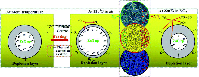
The gas sensing mechanism is illustrated in Fig. 8. At room temperature, the chemisorbed oxygen ions (O2−) (eqn (12)) were very few because the larger electronic depletion layer made the transfer of electrons difficult to the ZnO surface. Therefore, the sensitivity of ZnO was lower at room temperature. When ZnO is heated to 220 °C, according to the physics of semiconductors,37 the electron concentration (n0) of ZnO in the conduction band is shown in formula (11).
 | (11) |
| O2 (ads) + e− → O2− (ads) | (12) |
| NO2 (gas) + e− → NO2− (ads) | (13) |
| NO2 (gas) + O2− + 2e− → NO2− (ads) + 2O− | (14) |
When the ZnO nanowalls were exposed to NO2, which is a strong oxidizing molecule, the adsorbed NO2 gas molecules captured the electrons from the conduction band (eqn (13)) and reacted with O2− (eqn (14)), thereby increasing the depletion layer and resistance (Rg) of ZnO.38 The surface of the ZnO nanowalls supplied numerous active sites for adsorbing NO2. However, due to the lower density of the ZnO nanowalls (see Fig. 2(d), 4(a) and (b)), there were not many adsorption sites, and the larger density blocked the adsorption sites that were provided by the side of the ZnO nanowalls. Hence, the sensitivity was lower (see Fig. 7(b) and (c)). The ZnO nanowalls prepared by the ideal parameters (dipping for 4 times and growth time of 5 h) could supply the adsorption sites from the surface and sides. Therefore, the increase in the NO2 sensitivity was due to the reduced Ra, generating more free electrons and O2−, which led to a more sufficient reaction between ZnO and NO2.
4 Conclusion
In summary, we developed a ZnO film consisting of a seed layer of ZnO nanoparticles and a growth layer of the vertically grown ZnO nanosheets. The seed layer was formed by the continuous netted morphological Zn-HDS transforming to a granular ZnO nucleus. The ZnO formed by the chemical reaction was directly deposited on the seed layer to form ZnO nanowalls during solution growth at 80 °C. Al was mainly concentrated in the seed layer to block the ZnO growth along the c-axis direction and promote the lateral growth. The synthesis of the solution-grown ZnO nanowalls included 3 stages: (i) a quick growth stage, (ii) a slow growth stage, and (iii) an exponential decay growth stage. The sensitivity of the sensors presented a significant difference for NO2 gas sensing at different dipping times and growth times due to the numbers of ZnO nanowalls and 3D pore sizes. When the number of dipping times was 4 or the growth time was 5 h, the highest sensitivity was 36.64.5 Experimental sections
5.1 Sample preparation
The ZnO nanowalls were prepared by a solution method, which included four steps. The details are as follows:Step 1: Deposition of seed layer. 4.390 g of Zn(CH3COO)2 and 3.7512 g of Al(NO3)3·9H2O were added into 100 mL of ethyl alcohol and then, the solution was heated under stirring at 70 °C for 1 h. The Ag interdigitated electrode and ITO glass substrates were immersed with a constant speed (6000 μm min−1) and placed vertically in the solution for 30 s by a dip coating machine (SYDC-100H). Then, the samples were dried at 70 °C for 15 min. In order to study the effect of dipping times on the density of nucleation and morphology of the ZnO nanostructure, the dipping times were designed as 2, 4, 6, and 8 times.
Step 2: Annealing treatment of the seed layer. The samples (after Step 1) were annealed at 400 °C for 30 min. The heating rate was 2 °C min−1 from room temperature to 400 °C.
Step 3: Growth of ZnO nanowalls. 0.3512 g of C6H12N4 and 0.7438 g of Zn (NO3)2·6H2O were added into 50 mL of deionized water, agitated at 70 °C for 50 min, and ultrasonicated for 10 min. The samples (after Step 2) were placed vertically in the solution under 80 °C. In order to explore the morphology evolution of the ZnO nanostructure at different growth times, the growth times were 1 h, 2 h, 3 h, 4 h, 5 h and 8 h.
Step 4: Annealing treatment of the growth film. The samples (after Step 3) were annealed at 450 °C for 60 min. The heating rate was 2 °C min−1 from room temperature to 450 °C.
5.2 Characterization
The structural identification of the samples was carried out by an X-ray diffractometer (XRD, SHIMADZU-6000) with Cu-Kα radiation (λ = 0.154056 nm). The morphology of the samples was observed directly using a scanning electron microscope (SEM, FEI QAUANTA 400). The elemental composition of the samples was studied by EDS that was connected to SEM. FT-IR spectra (ATR) were recorded on Nicolet-380. A transmission electron microscope (TEM, JEOL 2100) was used to further investigate the microstructure of the samples at an accelerating voltage of 200 kV. The density of ZnO nucleation was defined as the percentage of the area occupied by the ZnO nanoparticles. The density (F = P2/(4πA)) and pore size (D = (4A/π)1/2), where A is the area of the particle and P is the perimeter of particle, were measured using image analysis software Image-Pro plus 6.0.5.3 Gas sensing measurement
The gas sensing performance of all samples was measured by a gas-sensing characterization system (CGS-1TP, Elite Instruments). The sensitivities (S) of the sensor were defined as Rg/Ra, where Ra is the resistance of the sensor without NO2 gas and Rg is the resistance within. The time taken by the sensor resistance to change from Ra to Rg − 90% × (Rg − Ra) was defined as the response time when the target gas was introduced to the sensor, and the time taken from Ra to Ra + 90% × (Rg − Ra) was defined as the recovery time when the ambience was replaced by air. The ambient humidity was controlled at 40% during the measurements.Conflicts of interest
The authors declare no conflicts of interest.Acknowledgements
This work was supported by the National Natural Science Foundation of China (21703134 and 51202177) and the Science & Research Fund of the Education Commission of Shaanxi Province (19JK0258).Notes and references
- S. W. Lee, W. Lee, Y. Hong, G. Lee and D. S. Yoon, Sens. Actuators, B, 2018, 255, 1788–1804 CrossRef CAS.
- J. M. Walker, S. A. Akbar and P. A. Morris, Sens. Actuators, B, 2019, 286, 624–640 CrossRef CAS.
- P. Tyagi, A. Sharma, M. Tonika and V. Gupta, Sens. Actuators, B, 2017, 248, 980–986 CrossRef CAS.
- P. S. Kolhe, A. B. Shinde, S. G. Kulkarni, N. Maiti, P. M. Koinkar and K. M. Sonawane, J. Alloys Compd., 2018, 748, 6–11 CrossRef CAS.
- Z. Y. Zhang, M. Haq, Z. Wen, Z. Z. Ye and L. P. Zhu, Appl. Surf. Sci., 2018, 434, 891–897 CrossRef CAS.
- S. F. H. Karouei and H. M. Moghaddam, Appl. Surf. Sci., 2019, 479, 1029–1038 CrossRef.
- D. Y. Fu, C. L. Zhu, X. T. Zhang, C. Y. Li and Y. J. Chen, J. Mater. Chem. A, 2016, 4, 1390–1398 RSC.
- P. Shankar and J. B. B. Rayappan, Sci. Lett. J., 2015, 4(1–18), 126 Search PubMed.
- O. Wurzinger and G. Reinhardt, Sens. Actuators, B, 2004, 103, 104–110 CrossRef CAS.
- A. M. Oyarun, A. J. A. S. Casanova, X. A. G. Carmona and L. R. Radovic, Carbon, 2016, 99, 472–484 CrossRef.
- Y. H. Zhang, X. L. Cai, L. Z. Song, F. Y. Feng, J. Y. Ding and F. L. Gong, J. Phys. Chem. Solids, 2019, 124, 330–335 CrossRef CAS.
- S. P. Xu, Y. Xu, H. P. Zhao, R. Xu and Y. Lei, ACS Appl. Mater. Interfaces, 2018, 10, 9092–29099 Search PubMed.
- K. J. Shah and T. Imae, Chem. Eng. J., 2016, 283, 1366–1373 CrossRef CAS.
- F. Y. Fan, P. G. Tang, Y. Y. Wang, Y. J. Feng, A. F. Chen, R. X. Luo and D. Q. Li, Sens. Actuators, B, 2015, 215, 231–240 CrossRef CAS.
- X. H. Liu, T. T. Ma, N. Pinna and J. Zhang, Adv. Funct. Mater., 2017, 27, 1702168 CrossRef.
- K. O. Iwu, V. Strano, A. D. Mauro, G. Impellizzeri and S. Mirabella, Cryst. Growth Des., 2015, 15(9), 4206–4212 CrossRef CAS.
- N. Islavath, D. Das, S. V. Joshi and E. Ramasamy, Mater. Des., 2017, 116, 219–226 CrossRef CAS.
- D. H. Kim, S. D. Lee, K. K. Kim, G. S. Park, J. M. Lee and S. W. Kim, J. Nanosci. Nanotechnol., 2008, 8, 4688–4691 CrossRef CAS PubMed.
- L. M. Yu, F. Guo, S. Liu, B. Yang, Y. X. Jiang, L. J. Qi and X. H. Fan, J. Alloys Compd., 2016, 682, 352–356 CrossRef CAS.
- L. M. Yu, J. S. Wei, Y. Y. Luo, Y. L. Tao, M. Lei, X. H. Fan, W. Yan and P. Peng, Sens. Actuators, B, 2014, 204, 96–101 CrossRef CAS.
- H. T. Ng, J. Li, M. K. Smith, P. Nguyen, A. Cassell, J. Han and M. Meyyappan, Science, 2003, 300(23), 1249 CrossRef CAS PubMed.
- S. Y. Gao, H. D. Li, J. J. Yuan, Y. A. Li, X. X. Yang and J. W. Liu, Appl. Surf. Sci., 2010, 256, 2781–2785 CrossRef CAS.
- M. S. Tokumoto, S. H. Pulcinelli, C. V. Santilli and V. Briois, J. Phys. Chem. B, 2003, 102, 568–574 CrossRef.
- A. Zieba, A. Pacula, E. M. Serwicka and A. Drelinkiewicz, Fuel, 2010, 89, 1961–1972 CrossRef CAS.
- H. Morioka, H. Tagaya, M. Karasu, J. I. Kadokawa and K. Chiba, J. Am. Chem. Soc., 1999, 38, 4211–4216 CAS.
- J. Lee, A. J. Easteal, U. Pal and D. Bhattacharyya, Curr. Appl. Phys., 2009, 9, 792–796 CrossRef.
- B. Saravanakumar and S. J. Kim, J. Phys. Chem. B, 2014, 118, 8831–8836 CAS.
- F. Grasset, O. Lavastre, C. Baudet, T. Sasaki and H. Haneda, J. Colloid Interface Sci., 2018, 317, 493–500 CrossRef PubMed.
- F. V. Molefe, L. F. Koao, B. F. Dejene and H. C. Swart, Opt. Mater., 2015, 46, 292–298 CrossRef CAS.
- L. M. Yu, F. Guo, Z. Y. Liu, S. Liu, B. Yang, M. L. Yin and X. H. Fan, Mater. Charact., 2016, 112, 224–228 CrossRef CAS.
- N. S. Harale, A. S. Kamble, N. L. Tarwal, I. S. Mulla, V. K. Rao, J. H. Kim and P. S. Patil, Ceram. Int., 2016, 42, 12807–12814 CrossRef CAS.
- N. B. Patil, A. R. Nimbalkar and M. G. Patil, Mater. Sci. Eng., B, 2018, 221, 53–60 CrossRef.
- X. X. Chen, Y. B. Shen, W. Zhang, J. Zhang, D. Z. Wei, R. Lu, L. J. Zhu, H. S. Li and Y. S. Shen, Appl. Surf. Sci., 2018, 435, 1096–1104 CrossRef CAS.
- P. Rai, S. Raj, K. J. Ko, K. K. Park and Y. T. Yu, Sens. Actuators, B, 2013, 178, 107–112 CrossRef CAS.
- R. Chen, J. Wang and L. Xiang, Sens. Actuators, B, 2018, 270, 207–215 CrossRef CAS.
- F. Y. Fan, Y. J. Feng, S. L. Bai, J. T. Feng, A. F. Chen and D. Q. Li, Sens. Actuators, B, 2013, 185, 377–382 CrossRef CAS.
- E. K. Liu, B. S. Zhu and J. S. Luo, The Physics of Semiconductors, Publishing House of Electronics Industry, Beijing, 2012 Search PubMed.
- B. X. Xiao, Q. Zhao, D. X. Wang, G. S. Ma and M. Z. Zhang, New J. Chem., 2017, 41, 8530–8535 RSC.
Footnote |
| † Electronic supplementary information (ESI) available. See DOI: 10.1039/c9ra07933e |
| This journal is © The Royal Society of Chemistry 2020 |

