Strain engineering the electronic and photocatalytic properties of WS2/blue phosphene van der Waals heterostructures†
Jingnan
Wang
a,
Yuhong
Huang
 *a,
Fei
Ma
 *b,
Jianmin
Zhang
a,
Xiumei
Wei
a and
Jing
Liu
c
aSchool of Physics & Information Technology, Shaanxi Normal University, Xi'an 710119, Shaanxi, China. E-mail: huangyh@snnu.edu.cn; Tel: +86 29 81530750
bState Key Laboratory for Mechanical Behavior of Materials, Xi'an Jiaotong University, Xi'an 710049, Shaanxi, China. E-mail: mafei@mail.xjtu.edu.cn; Tel: +86 29 82668610
cDepartment of Basic Sciences, Air Force Engineering University, Xi'an 710051, Shaanxi, China
First published on 27th October 2020
Abstract
The effects of −8–8% in-plane uniaxial and biaxial strains on the electronic and photocatalytic activity of tungsten disulfide/blue phosphene (WS2/BlueP) are investigated within the framework of first-principles calculations. The most energetically stable configuration of WS2/BlueP exhibits type I band alignment with a direct band gap of 1.779 eV. Compared with WS2 and BlueP, WS2/BlueP has the strongest absorption in the entire visible light region with a red-shifted absorption edge. The in-plane −8–8% uniaxial and biaxial strains cause elastic deformation of the heterostructures. The strains can affect the band gap, band edge arrangement, band type (type-I, type-II, Z-scheme) and electron transition type (direct, indirect) of WS2/BlueP. The −2% uniaxial (or biaxial) strain can engineer the band gap to reach the maximum and achieve full water decomposition. At pH = 0, only the −2% and −4% uniaxial and −2% biaxial strained WS2/BlueP (Z-scheme) heterostructures are thermodynamically feasible, while at pH = 7, all the strained heterostructures are viable for photocatalytic water decomposition. The −2% uniaxial and biaxial strained WS2/BlueP heterostructures at pH = 0 and pH = 7 are proved to be potential candidates for achieving full water decomposition. The lower potential determining step, higher electro-chemical driving forces and lower effective mass of carriers can promote the transition performance and improve the photocatalytic efficiency. Therefore, the in-plane uniaxial and biaxial strains can effectively adjust the electronic and photocatalytic performances of the heterostructures.
1. Introduction
Since the successful mechanical exfoliation from graphite in 2004,1 two-dimensional (2D) graphene has attracted worldwide attention due to its fascinating physical properties, such as unique hexagonal symmetry structure,2 extremely high carrier mobility3 and anomalous quantum Hall effect.4 Unfortunately, the zero band gap has greatly limited the practical application of graphene. Meanwhile, other 2D materials varying from insulators to semiconductors and semimetals have been explored, such as bismuth oxyhalides (BiOBr),5 transition metal dichalcogenides (TMDs)6 and phosphenes,7–9 which possess large specific surface area, high surface activity and excellent photocatalytic properties.10 S. V. Prabhakar Vattikuti et al. found that the hexagonal WS2 nanosheet has good photocatalytic activity for degrading rhodamine B under visible light irradiation. WS2 has a suitable band gap of 1.91 eV and can be mechanically peeled easily due to its weak van der Waals (vdW) interactions in the layered S–W–S sandwich structure.11 However, the large effective mass and low carrier mobility have hindered its real application in the photocatalytic field. Moreover, it can only achieve the oxygen evolution reaction (OER) since the reduction and oxidation potentials are 0.08 eV and 1.99 eV, respectively. Strain is one of the effective ways to adjust the electronic and optical properties of WS2 to meet the photocatalytic requirements. For instance, as the tensile strain on 1T-WS2 reaches 2.7%, the electron state density near the Fermi level increases significantly, and the free energy of adsorbed atomic hydrogen is close to thermoneutral (ΔGH ≈ 0), which is the benchmark of a good catalyst. In contrast, even when the strain on 2H–WS2 increases to 4%, the free energy remains at about 2 eV, presenting great thermodynamic resistance to hydrogen production.Recently, large-scale blue phosphorus (BlueP) monolayers on Au (111) and GaN (001) substrates12,13 were fully synthesized via molecular beam epitaxy. BlueP exhibits extremely high carrier mobility and can achieve water decomposition as an ideal photocatalyst with a reduction and oxidation center of −0.47 eV and 2.27 eV, respectively.14 However, the photocatalytic efficiency is greatly limited by an inherent band gap of 2.74 eV, resulting in ultraviolet absorption. Moreover, the poor stability limits its application in an open-air environment.15,16
For the sake of better performance, researchers have thought of stacking two-dimensional materials together to form a heterostructure, which not only has the properties of each constituent monolayer, but also exhibits significant electronic and optical properties missing in isolated monolayers.17 The “face-to-face” stacked heterostructure has a larger interface area and stronger electronic couplings between the layers, which can improve the electronic properties18 and eliminate the surface pollution.19 Supposing WS2 (strong absorption, weak redox ability) and BlueP (weak absorption, strong redox ability) are constructed to form a heterostructure, they can complement each other, achieve strong absorption and exhibit redox capabilities. Moreover, BlueP and WS2 have a small interface mismatch due to the same hexagonal structures with similar lattice constants, which can effectively reduce the dangling bonds and interface states. Qiong Peng et al. found that the WS2/BlueP heterostructure exhibits abnormally strong absorption rate and energy conversion efficiency in the visible light range.20
Previous experimental and theoretical studies have shown that in-plane uniaxial and biaxial strains can further effectively adjust the band gap, absorption, charge transfer and redox capabilities of nanosheets or heterostructures, such as Ga2SSe,21 SnSe2,22 MoSe2/PtS2 (ref. 23) and PtS2/MoS2.24 Long Lin et al. found that the biaxial strain on the group VA/VA 2D vdW heterostructures can convert the indirect band gap into a direct one, and finally cause the heterostructure to become metal with excellent electrical conductivity.25 Jiaxin Ye et al. found that the in-plane biaxial tensile strain on g-C3N4/WSe2 can reduce the band gap and promote the red-shift of the absorption peak.26 Xiaolong Wang et al. found that strain can adjust the energy band arrangement of C2N/MTe (M = Ga, In) heterostructures and improve the redox potential.27 Afterwards, Wenxue Zhang et al. found that the plane biaxial strain not only maintains the high carrier mobility of BlueP/WS2, but also changes the band structure from type-II to type-I as a potential photocatalytic switch.28 So far, the Heyd–Scuseria–Ernzerhof 2006 (HSE06) hybrid functional has not been used to discuss the electronic and photocatalytic properties of WS2/BlueP heterostructures, nor have there been any studies to adjust the photocatalytic activity of WS2/BlueP heterostructures by in-plane uniaxial and biaxial strains.
Therefore, in-plane uniaxial and biaxial strains within the range of −8–8% are applied to investigate the influences of strain on the WS2/BlueP heterostructure. The electronic and optical properties including the band structure, density of states, light absorption, charge density difference, band arrangement, the carrier mobility are systematically analyzed. Furthermore, the photocatalytic properties is investigated and in particular the Gibbs free energy (ΔG) during the OER process is calculated to explore the thermodynamic feasibility of photocatalytic water splitting. The conclusions might help people to find and design photocatalysts with excellent performance for photocatalytic water splitting.
2. Computational methods
The electronic, optical and photocatalytic properties of WS2, BlueP nanosheets and WS2/BlueP heterostructures are explored based on the density functional theory, which is performed using the Vienna ab initio simulation package (VASP)29,30 with the projector augmented wave (PAW). The generalized gradient approximation (GGA) of the Perdew–Burke–Ernzerhof (PBE) functional is used to deal with the exchange–correlation interactions between the electrons.31 The optB88-vdW functional is adopted to evaluate the vdW interaction, where the exchange functionals were optimised for the correlation part.32,33 The cut-off energy of the plane-wave basis is set to be 400 eV. The WS2/BlueP heterostructures are fully relaxed until the force and the total energy decrease to −0.02 eV Å−1 and 1 × 10⁻⁴ eV, respectively. A vacuum spacing of 25 Å is added to avoid the interlayer interactions caused by the periodicity along the direction perpendicular to the 2D nanosheets.While calculating the electronic properties, the Heyd–Scuseria–Ernzerhof (HSE06) hybrid functional is adopted to avoid the underestimation of the band gap by the PBE functional. The exchange–correlation energy EHSEXC in the HSE06 function is given by34–36EHSEXC = αESRX(μ) + (1 − α)EPBE,SRX(μ) + EPBE,LRX(μ) + EPBEC, where α is taken as the default value of 0.25, the SR and LR stand for short-ranged and long-ranged parts of the electron–electron interactions, and the screening parameter μ is the ratio of SR and LR, which is set as 0.20 Å−1.
3. Results and discussion
3.1 Geometric configurations and interface formation energy
Fig. 1a and b show the fully relaxed structure of WS2 and BlueP nanosheets, with lattice constants of 3.185 Å and 3.278 Å, respectively, which are consistent with the previous results.20,37 For the construction of ideal heterostructures, the lattice constants of constituent materials should match as well as possible, however, a mismatch is inevitable, which will induce large dangling bonds, interfacial states and stress.38,39 The heterostructure is constructed with 3 × 3 supercells of WS2 and BlueP nanosheets. Fig. 1c–f show four optimized stacking patterns of WS2/BlueP: (I) S atoms are on top of the hollow sites of BlueP, (II) P–P bonds and W–S bonds cross each other from the top view, (III) P atoms are exactly on top of W and S sites, (IV) W atoms are on top of the hollow sites of BlueP.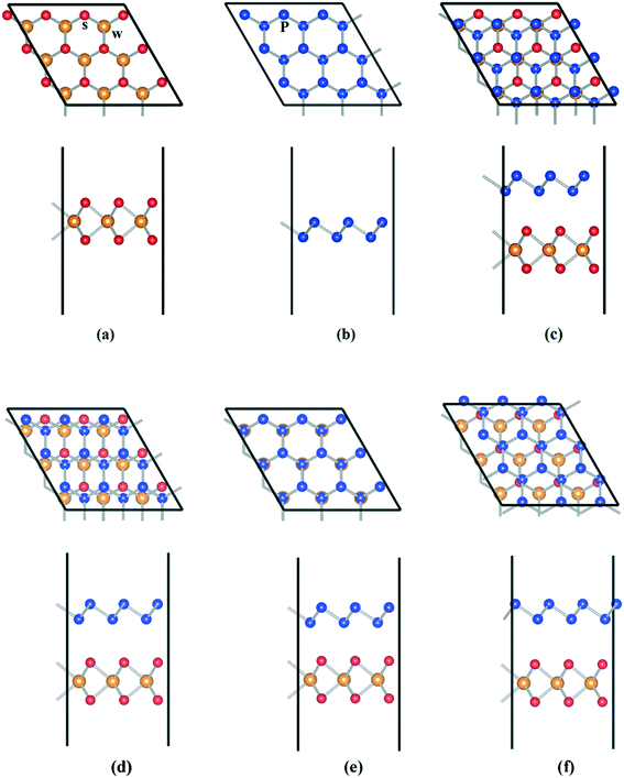 | ||
| Fig. 1 The relaxed geometrical configurations of WS2 (a), BlueP nanosheets (b) and WS2/BlueP heterostructures of model I (c), II (d), III (e) and IV (f). | ||
The interface formation energy is utilized to evaluate the stability of the heterostructure, which is defined as:40
| Ef = EWS2/BlueP − EWS2 − EBlueP | (1) |
The interface binding energies of four configurations of WS2/BlueP are calculated by the absolute value of Ef per unit interface area.
According to eqn (1), the formation and binding energies of four configurations of WS2/BlueP are obtained and shown in Table 1. It can be found that the formation energies are all less than 0, indicating that the formation processes are exothermic and they are stable. Among them, the configuration of model III has the smallest formation energy, proving that this heterostructure is the most stable one. The binding energies are all in the range of the typical vdW binding energy (13–21 meV Å−2), indicating that WS2/BlueP has a typical vdW heterostructure. Hence, WS2/BlueP of model III is chosen for further investigation in the following context. The corresponding lattice mismatch is calculated by η = 2(a1 − a2)/(a1 + a2), where α1 and α2 are the lattice parameters of WS2 and BlueP nanosheets, respectively. The lattice mismatch is estimated to be 2.88%, which is acceptable (<5%) to create vdW heterostructures. The minimum distance (d) between the interfacial layers of WS2/BlueP is 3.22 Å, which is in the range of the vdW interaction distance (3–5 Å), indicating that WS2/BlueP belongs to typical vdW heterostructure.
| Model I | Model II | Model III | Model IV | |
|---|---|---|---|---|
| E f (eV) | −1.507 | −1.317 | −1.663 | −1.171 |
| E b (meV Å−2) | 18.176 | 15.886 | 20.058 | 14.121 |
3.2 Optoelectronic properties
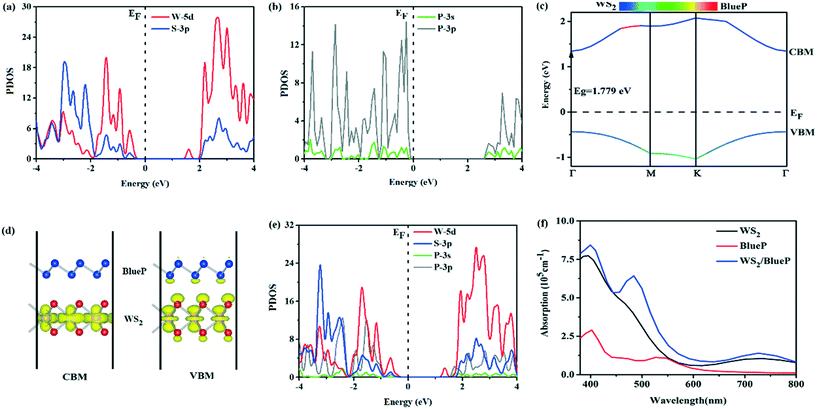
The band gaps of WS2 and BlueP nanosheets are 2.037 eV and 2.910 eV, respectively. The projected density of state (PDOS) shows that the orbitals near the Fermi level are mainly occupied by W-5d of WS2 (Fig. 2a) and P-3p of the BlueP nanosheet (Fig. 2b). The valence band maximum (VBM) and the conduction band minimum (CBM) of the WS2/BlueP heterostructure are both located at high symmetry k-point Γ, showing a direct band gap of 1.779 eV, which is smaller than the band gaps of WS2 and BlueP. The direct transition without the phonon's participation makes WS2/BlueP respond to visible light. Moreover, the band gap is greater than the minimum energy (1.23 eV) required by thermodynamics, making it an ideal candidate in photocatalysis (Fig. 2c). The band decomposed charge density (Fig. 2d) shows that the CBM and VBM are mainly contributed by W atoms in the WS2 layer, besides, the VBM is also contributed by a small amount of S atoms in WS2 and P atoms in BlueP. Meanwhile, the S atoms on each side of the isolated WS2 have similar electronic states due to the symmetric configuration. However, it is completely different in the heterostructure, the corresponding energy band is not a simple superposition of the isolated WS2 and BlueP, which is mainly affected by the interfacial interactions and charge transfer resulting in the shift of the electronic states. The PDOS of WS2/BlueP (Fig. 2e) further points out that the VBM is mainly occupied by W-5d with a small degree of hybridization of S-3p and P-3p, however, the CBM is totally occupied by the W-5d orbital, demonstrating that the WS2/BlueP heterostructure has a type-I band arrangement.In order to decompose water efficiently by photocatalysts, it is expected that light absorption covers a significant portion of the visible spectrum (380–780 nm). The light response range of WS2/BlueP is expanded as shown in the absorption spectra (Fig. 2f), and the absorption intensity in the entire visible light region is greater than that of WS2 and BlueP. The enhanced light absorption may be caused by the overlap of the electronic states in the VB of the heterostructure due to the charge redistribution and interface coupling. Moreover, the absorption edge is red-shifted. The excellent optical performance will improve the photoelectric conversion efficiency and the photocatalytic activity of WS2/BlueP.
The electrons participate in the redox reaction via transition from the Fermi level (inside) to the vacuum level (surface), and the required minimum energy is the work function, which is defined as:
| ϕ = Evac − EF | (2) |
3.3 Interfacial electronic and photocatalytic properties
There is no doubt that WS2/BlueP has different interfacial electronic properties with respect to the surfaces of the isolated nanosheets, which may be caused by the atomic electronegativity and charge redistribution. Since the S atom has a greater electronegativity (6.22 eV) than the P atom (5.62 eV),41 the lone pair of electrons on the lower surface of BlueP is pulled closer to the upper surface of WS2, which makes the electrons (holes) accumulate on the upper (lower) surface of WS2 (BlueP), and thereby forms a built-in electric field. The charge redistribution is reflected by the three-dimensional charge density difference (Δρ) and the planar-averaged charge density difference along the Z direction (Δρavg(z)), which is defined as| Δρ = ρWS2/BlueP − ρWS2 − ρBlueP | (3) |
 | (4) |
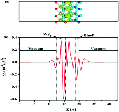 | ||
| Fig. 3 The side view of the three-dimensional charge density difference (a) and the planar-average charge density difference perpendicular to the Z direction of WS2/BlueP (b). | ||
The photocatalytic activity of the material is estimated by the energy band arrangement, which is related to the position of the CBM (ECB) and VBM (EVB) versus the vacuum level, expressed as follows:
| ECB = −χ + 0.5Eg | (5) |
| EVB = −χ − 0.5Eg | (6) |
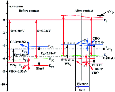 | ||
| Fig. 4 The equilibrium energy band arrangement of WS2 and BlueP nanosheets before and after contact. | ||
3.4 Strain effects on the electronic properties of WS2/BlueP
The in-plane uniaxial and biaxial strains can effectively adjust the electronic properties of 2D heterostructures, which can be achieved by adjusting the lattice parameters of the heterostructures. The strain is evaluated by:| ε = (a − a0)/a0 × 100% = Δa/a0 × 100% | (7) |
The strain energy is defined as:
| Es = Estrain − Eideal | (8) |
The in-plane uniaxial and biaxial strains in the range of −8% to 8% are chosen to study their effects on the band gaps of WS2/BlueP. The variations of strain energies and band gaps with different tensile and compressive strains are shown in Fig. 5. The relationship of strain energy and strain can be approximately stated with a quadratic function, demonstrating that the system has undergone elastic deformation, and the applied strains are within the elastic limit (Fig. 5a and b). That is to say, the heterostructure can be stretched and compressed in a reversible way and it will be restored to the original state as the strain is reduced to zero. Fig. 5c and d show that, both the −2% and −4% uniaxial and biaxial strains can enlarge the band gaps, while the other strains diminish them compared with WS2/BlueP free of strain. Notably, the band gap reaches the maximum as the heterostructure is under the −2% uniaxial (or biaxial) strain.
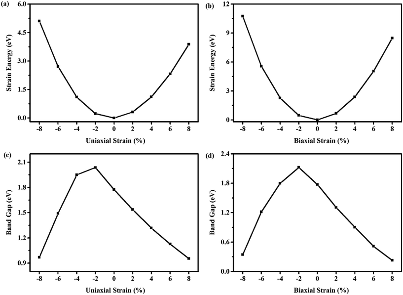 | ||
| Fig. 5 The strain energy and the band gap as a function of the uniaxial strain (a and c) and biaxial strain (b and d). | ||
The applied external strain is also one of the effective ways to adjust the band edge arrangement. Under the uniaxial and biaxial strains, the CBM and VBM of BlueP and WS2 in WS2/BlueP, as shown in Fig. 6, are compared with each other and the band edge arrangement can be summarized into four categories: (I) CBMBlueP < CBMWS2, VBMBlueP > VBMWS2, (II) CBMBlueP > CBMWS2, VBMBlueP > VBMWS2, (III) CBMBlueP > CBMWS2, VBMBlueP < VBMWS2, (IV) CBMBlueP < CBMWS2, VBMBlueP < VBMWS2. The specific comparisons between the CBM and VBM of BlueP and WS2 under each strain are marked with mathematical symbols “<” and “>” as shown in Table 2. According to the band arrangement, the electron transition type and the band type are obtained and listed in Table 2. The −4%, −6%, −8% and 8% uniaxial strains alter the direct bandgaps of WS2/BlueP to indirect ones, while the other strains maintain the same direct bandgaps as the ideal WS2/BlueP. The indirect transition needs the assistance of phonons to excite the electrons from the VBM to CBM, which is unfavourable for the generation of carriers. Remarkably, even the same transition type of the electron does not necessarily correspond to the same band type. The band types of the ideal and strained WS2/BlueP can be categorized as type-I, type-II and Z-scheme, which may be caused by the strains with different magnitudes and loading modes. It is worth noting that there are two cases of type I band arrangement: (I) CBMBlueP < CBMWS2, VBMBlueP > VBMWS2 due to the −8%, −6% uniaxial and −4% biaxial strains and (II) CBMBlueP > CBMWS2, VBMBlueP < VBMWS2 due to the 2%, 6% and 8% uniaxial and biaxial strains. The type-II heterostructures correspond to the band arrangement of CBMBlueP < CBMWS2, VBMBlueP < VBMWS2 resulting from the −8% and −6% biaxial strains, while the Z-scheme heterostructures correspond to the case of CBMBlueP > CBMWS2, VBMBlueP > VBMWS2 resulting from the −2% and −4% uniaxial strains and −2% biaxial strain.
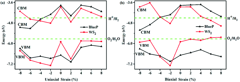 | ||
| Fig. 6 The band edges (CBM and VBM) of each constituent in WS2/BlueP under the uniaxial strain (a) and biaxial strain (b). | ||
| Strain (%) | BlueP versus WS2 | Transition type | Band type | ||
|---|---|---|---|---|---|
| CBM | VBM | ||||
| Uniaxial strain | −8, −6 | < | > | Indirect | Type-I |
| −4 | > | > | Indirect | Z-Scheme | |
| −2 | > | > | Direct | Z-Scheme | |
| 2, 6 | > | < | Direct | Type-I | |
| 8 | > | < | Indirect | Type-I | |
| Biaxial strain | −8, −6 | < | < | Direct | Type-II |
| −4 | < | > | Direct | Type-I | |
| −2 | > | > | Direct | Z-Scheme | |
| 2, 6, 8 | > | < | Direct | Type-I | |
The type-I heterostructure is disadvantageous to the separation of photogenerated carriers because the reduction (Re) and oxidation (Ox) centers are located in the same layer. In contrast, the Re and Ox centers of the type-II and Z-scheme heterostructures are located in different layers, which can effectively separate the photogenerated carriers in space and greatly improve the photocatalytic activity of the heterostructures. Therefore, in the subsequent context, we only focus on the type II and Z-scheme heterostructures involving the −2% and −4% uniaxial strains and −2%, −6%, and −8% biaxial strains.
The band edges and carrier transfer pathways of the −2% and −4% uniaxial and −2% biaxial strained WS2/BlueP (Fig. 7a) show that as WS2 and BlueP absorb the solar energies greater than their band gaps, the electrons will transition from the VB to the corresponding CB, leaving an equal number of holes in the VB. The energy band offset promotes the electrons to transfer from the CB of BlueP to WS2 and the holes from the VB of WS2 to BlueP. However, the built-in electric field impedes this kind of movement, and promotes the electrons from the CB of WS2 to recombine with the holes from the VB of BlueP. Therefore, a large number of electrons and holes are separated and accumulated in the CB of BlueP and VB of WS2, which become the Re and Ox centers, respectively. The above analyzed mechanism indicates the −2% and −4% uniaxial and −2% biaxial strained WS2/BlueP belong to the typical direct Z-scheme photocatalysts.
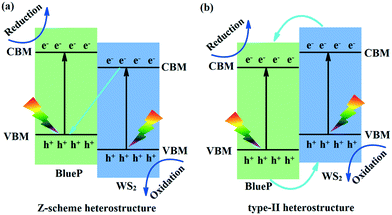 | ||
| Fig. 7 Schematic diagrams of the band edges and carrier transfer pathways of the Z-scheme (a) and type-II (b) heterostructures. | ||
The band edges and carrier transfer pathways of the −6% and −8% biaxial strained WS2/BlueP (Fig. 7b) show that both the band offset and the built-in electric field promote the electrons to transfer from the CB of WS2 to BlueP and the holes from the VB of BlueP to WS2, thus a large number of electrons and holes are accumulated in the CB of BlueP and VB of WS2, which become the Re and Ox centers, respectively. Therefore, the −6% and −8% biaxial strained WS2/BlueP heterostructures are type-II photocatalysts. It is worth noting that the Re and Ox centers of the Z-scheme WS2/BlueP are relatively higher than those of type-II heterostructures due to the applied strains, demonstrating that the direct Z-scheme photocatalysts have higher oxidation and reduction capabilities, which will be better candidates for optoelectronic devices.
The planar-average charge density difference along the Z direction of uniaxial (−2% and −4%) and biaxial (−2%, −6%, and −8%) strained WS2/BlueP shows that, near the interface, BlueP loses and WS2 gains electrons, which is similar to the case of the ideal heterostructure. The directional movement of the electrons forms the space charge region together with a built-in electric field pointing from BlueP to WS2. This indicates that the strains do not reverse the built-in electric field. Bader charge analysis further provides the amount of charge transfer across the interface (Table 2), which demonstrates that the −2% and −4% uniaxial and −2% biaxial strained WS2/BlueP heterostructures have more charge transfer than the ideal one, indicating that the strain induced built-in electric field is stronger and the corresponding heterostructures can separate the photogenerated carriers more efficiently. This is mainly caused by the stronger interfacial interactions due to the smaller interlayer distances as shown in Table 2, thus the electrons pass through the interface easily. In contrast, with respect to ideal WS2/BlueP, the −6% and −8% biaxial strains have less charge transfer due to the larger interlayer distances, which reduces the interfacial interactions and is not conducive to the charge movement (Fig. 8).
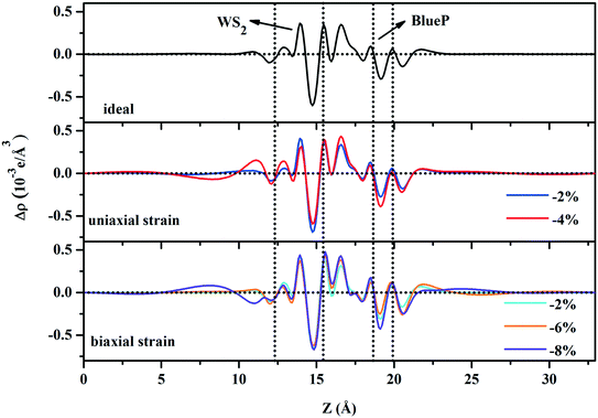 | ||
| Fig. 8 The planar-average charge density difference along the Z-direction of ideal, uniaxial and biaxial strained WS2/BlueP heterostructures. | ||
3.5 Strain effects on the photocatalytic properties
As is well known the Re center of a catalyst should be greater than H+/H2 (−4.5 eV), and the Ox center should be less than O2/H2O (−5.73 eV) referring to full water decomposition. Analyzing the Re and Ox centers of strained WS2/BlueP in Table 3, it can be seen that both the −2% uniaxial and biaxial strains lead to strong reduction capacities (Re > −4.5 eV) of the heterostructures, which can easily undergo the hydrogen evolution reaction (HER), while the −4% uniaxial and −6% and −8% biaxial strained heterostructures cannot undergo such reactions spontaneously. To adjust the Re centers of the heterostructures, in general, the cocatalyst is added during the reaction process in the experiment. The Ox centers of strained WS2/BlueP are all less than −5.73 eV, which is beneficial to the OER and the degradation of organic pollutants. Therefore, −2% uniaxial and biaxial strains can achieve full water decomposition.| Physical quantity | Uniaxial strain | Biaxial strain | ||||
|---|---|---|---|---|---|---|
| −2% | −4% | −2% | −6% | −8% | ||
| Bader (e) | −0.140 | −0.140 | −0.136 | −0.124 | −0.121 | |
| d (Å) | 3.206 | 3.192 | 3.191 | 3.248 | 3.225 | |
| Re center (eV) | −4.298 | −4.574 | −3.615 | −4.899 | −5.216 | |
| Ox center (eV) | −7.283 | −7.144 | −7.288 | −5.816 | −5.923 | |
| pH = 0 | PDS (eV) | 0.585 | 0.639 | 0.610 | 0.527 | 0.607 |
| EDF (eV) | 1.553 | 1.414 | 1.558 | 0.086 | 0.193 | |
| pH = 7 | PDS (eV) | 0.172 | 0.226 | 0.197 | 0.114 | 0.194 |
| EDF (eV) | 1.966 | 1.827 | 1.971 | 0.499 | 0.606 | |
| m e/m0 | 0.132 | 0.183 | 0.354 | 0.162 | 0.150 | |
| m h/m0 | 0.590 | 0.770 | 0.314 | 0.970 | 0.177 | |
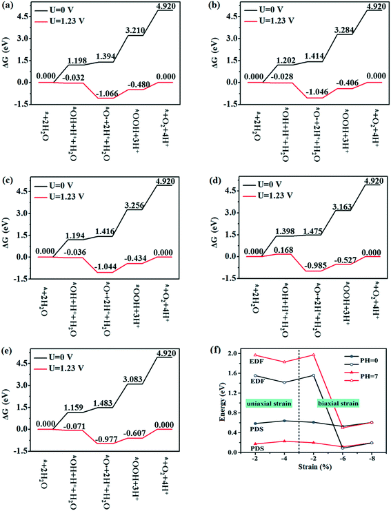
The thermodynamic feasibility is crucial to photocatalytic water splitting, and the HER is relatively easy under the influence of potential, therefore, the feasibility of the OER in thermodynamics is only considered. As U = 0 V, 1.23 V (minimum potential difference required for water decomposition) and pH = 0, the variation of Gibbs free energy ΔG with reaction steps of *H2O, *OH, *O, *OOH and O2 release are shown in Fig. 9a–e, where ‘*’ stands for the substrate (WS2/BlueP). As U = 0 V and pH = 0, ΔG goes up with each step of the reaction, and eventually reaches 4.920 eV for all the strained heterostructures. For each strained WS2/BlueP, the curve of U = 1.23 V and pH = 0 is obtained by ΔGU=1.23 = ΔGU=0 −1.23. The potential determining step (PDS) is adopted to evaluate the feasibility of the OER, which refers to the largest energy difference of every two adjacent steps at U = 1.23 V. The values of the PDS for −2% and −4% uniaxial and −2%, −6%, and −8% biaxial strained WS2/BlueP are obtained and listed in Table 3. This shows that the −6% biaxial strained WS2/BlueP heterostructure has the smallest PDS, indicating that it is the best choice for achieving the OER. Notably, in the case of pH = 7, the correction term ΔGpH = −KbT![[thin space (1/6-em)]](https://www.rsc.org/images/entities/char_2009.gif) ln
ln![[thin space (1/6-em)]](https://www.rsc.org/images/entities/char_2009.gif) 10 × pH = −0.059 pH should be considered during the calculation of the ΔG and PDS. As shown in Table 3, the ΔGU=1.23 declines in the first and second reactions while increases in the third and fourth reactions except −6% biaxial strained WS2/BlueP, where ΔGU=1.23 only decreases in the second reaction. The actual electrochemical driving forces (EDFs) of the OER are calculated as (ENHEVBM − 1.23) and (ENHEVBM − 1.23 + 0.059 × pH) for pH = 0 and pH = 7, respectively, where the NHE refers to the normal hydrogen electrode. The calculated values of the EDF are listed in Table 3. Our analytic conclusion suggests that when the EDF is equal or greater than the PDS, the ΔG of each reaction step is equal or less than zero, thus the OER can be conducted spontaneously. As shown in Fig. 9f, the values of the EDF at pH = 0 are greater than the PDS for −2% and −4% uniaxial and −2% biaxial strained WS2/BlueP, which indicates that the Z-scheme heterostructure is feasible in thermodynamics for photocatalytic water decomposition. In contrast, the EDF of −6%, −8% biaxial strained WS2/BlueP (type II) is less than the PDS, indicating that the external energy is needed to achieve water decomposition. The above conclusion further demonstrates that the Z-scheme heterostructure is a better choice for photocatalytic water splitting due to its stronger oxidation and reduction potential. When pH = 7, the values of the EDF are greater than the PDS for all the strained heterostructures, which proved to be thermodynamically feasible during photocatalytic water decomposition. Therefore, it is an effective way to improve the photocatalytic activity of the strained heterostructure by adjusting the pH value.
10 × pH = −0.059 pH should be considered during the calculation of the ΔG and PDS. As shown in Table 3, the ΔGU=1.23 declines in the first and second reactions while increases in the third and fourth reactions except −6% biaxial strained WS2/BlueP, where ΔGU=1.23 only decreases in the second reaction. The actual electrochemical driving forces (EDFs) of the OER are calculated as (ENHEVBM − 1.23) and (ENHEVBM − 1.23 + 0.059 × pH) for pH = 0 and pH = 7, respectively, where the NHE refers to the normal hydrogen electrode. The calculated values of the EDF are listed in Table 3. Our analytic conclusion suggests that when the EDF is equal or greater than the PDS, the ΔG of each reaction step is equal or less than zero, thus the OER can be conducted spontaneously. As shown in Fig. 9f, the values of the EDF at pH = 0 are greater than the PDS for −2% and −4% uniaxial and −2% biaxial strained WS2/BlueP, which indicates that the Z-scheme heterostructure is feasible in thermodynamics for photocatalytic water decomposition. In contrast, the EDF of −6%, −8% biaxial strained WS2/BlueP (type II) is less than the PDS, indicating that the external energy is needed to achieve water decomposition. The above conclusion further demonstrates that the Z-scheme heterostructure is a better choice for photocatalytic water splitting due to its stronger oxidation and reduction potential. When pH = 7, the values of the EDF are greater than the PDS for all the strained heterostructures, which proved to be thermodynamically feasible during photocatalytic water decomposition. Therefore, it is an effective way to improve the photocatalytic activity of the strained heterostructure by adjusting the pH value.
The applied strains can also adjust the transfer rate of the photogenerated carriers, reflected by the carrier mobility (μ) under an electric field, which is defined as:
 | (9) |
4. Conclusions
In summary, the effects of in-plane uniaxial and biaxial strains on the electronic and photocatalytic activity of WS2/BlueP are systematically studied through first-principles calculations. The most energetically stable configuration of WS2/BlueP is “P atoms exactly on top of W and S sites” (model III), which exhibits a direct band gap of 1.779 eV, and both the VBM and CBM are occupied by W-5d, with the characteristic of type I heterostructure. Moreover, WS2/BlueP not only expands the light response to the entire visible light region, but also enhances the absorption intensity and red-shifts the absorption edge. The charge density difference, work function and Bader analysis can prove the built-in electric field pointing from BlueP to WS2. The WS2/BlueP is further confirmed as a type-I heterostructure by the band arrangement, and its redox centers are located in the WS2 layer, which is not conducive to the separation of carriers.The in-plane −8–8% uniaxial and biaxial strains make the heterostructure undergo elastic deformation. The strains can affect the band gap, band edge arrangement, band type (type-I, type-II, Z-scheme) and electron transition type (direct, indirect) of WS2/BlueP, even though the same electron transition type does not correspond to the same band type. The −2% uniaxial (or biaxial) strain can engineer the band gap to reach the maximum and achieve full water decomposition. At pH = 0, only the −2% and −4% uniaxial and −2% biaxial strained WS2/BlueP (Z-scheme) heterostructures are thermodynamically feasible for photocatalytic water splitting, while at pH = 7, all the strained heterostructures are feasible. Hence, it is an effective way to improve the photocatalytic activity by adjusting the pH value of the strained heterostructures. The −2% uniaxial and biaxial strained WS2/BlueP are potential candidates for electron-driven HER and hole-driven OER, respectively. Moreover, the lower PDS, EDF and m* values can promote the transition performance and improve the photocatalytic reaction efficiency. In conclusion, the electronic and photocatalytic properties of WS2/BlueP can be engineered by in-plane uniaxial and biaxial strains.
Conflicts of interest
There are no conflicts to declare.Acknowledgements
This work was supported by the National Natural Science Foundation of China (No. 51771144), the Natural Science Foundation of Shaanxi Province in China (No. 2017JZ015), the Fundamental Research Funds for the Central Universities (No. GK GK202003017, 2019CSLY004) and the Comprehensive Teaching Reform Research Project of Shaanxi Normal University (No. 19JG27).References
- X. Gao, Y. Shen, Y. Ma, S. Wu and Z. Zhou, First-principles insights into efficient band gap engineering of the blue phosphorus/g-C3N bilayer heterostructure via an external vertical strain, Appl. Surf. Sci., 2019, 479, 1098–1104 CrossRef CAS.
- X. Wang, X. Yang, B. Wang, G. Wang and J. Wan, Significant band gap induced by uniaxial strain in graphene/blue phosphorene bilayer, Carbon, 2018, 130, 120–126 CrossRef CAS.
- A. K. Geim and K. S. Novoselov, The rise of graphene, Nanosci. Technol., 2009, 11–19 Search PubMed.
- Y. Zhang, Y. W. Tan, H. L. Stormer and P. Kim, Experimental observation of the quantum Hall effect and Berry's phase in graphene, Nature, 2005, 438, 201–204 CrossRef CAS.
- M. M. Obeid, C. Stampfl, A. Bafekry, Z. Guan, Z. H. R. Jappor, C. V. Nguyen, M. Naseri, D. M. Hoat, N. N. Hieu, A. E. Krauklis, T. V. Vu and D. Gogova, First-principles investigation of nonmetal doped single-layer BiOBr as a potential photocatalyst with a low recombination rate, Phys. Chem. Chem. Phys., 2020, 22(27), 15354–15364 RSC.
- Y. Cai, G. Zhang and Y. W. Zhang, Electronic properties of phosphorene/graphene and phosphorene/hexagonal boron nitride heterostructures, J. Phys. Chem. C, 2015, 119, 13929–13936 CrossRef CAS.
- L. Li, Y. Yu, G. J. Ye, Q. Ge, X. Ou, H. Wu, D. Feng, X. H. Chen and Y. Zhang, Black phosphorus field-effect transistors, Nat. Nanotechnol., 2014, 9, 372–377 CrossRef CAS.
- H. O. Churchill and P. Jarillo-Herrero, Two-dimensional crystals: phosphorus joins the family, Nat. Nanotechnol., 2014, 9, 330–331 CrossRef CAS.
- A. Goswami and M. B. Gawande, Phosphorene: current status, challenges and opportunities, Front. Chem. Sci. Eng., 2019, 13(2), 296–309 CrossRef.
- S. L. Li, K. Tsukagoshi, E. Orgiu and P. Samorì, Charge transport and mobility engineering in two-dimensional transition metal chalcogenide semiconductors, Chem. Soc. Rev., 2016, 45, 118–151 RSC.
- Q. H. Wang, K. Kalantar-Zadeh, A. Kis, J. N. Coleman and M. S. Strano, Electronics and optoelectronics of two-dimensional transition metal dichalcogenides, Nat. Nanotechnol., 2012, 7, 699–712 CrossRef CAS.
- J. L. Zhang, S. Zhao, C. Han, Z. Wang, S. Zhong, S. Sun, R. Guo, X. Zhou, C. D. Gu, K. D. Yuan, Z. Li and W. Chen, Epitaxial growth of single layer blue phosphorus: a new phase of two-dimensional phosphorus, Nano Lett., 2016, 16, 4903–4908 CrossRef CAS.
- J. Zeng, P. Cui and Z. Zhang, Half layer by half layer growth of a blue phosphorene monolayer on a GaN(001) substrate, Phys. Rev. Lett., 2017, 118, 046101 CrossRef.
- B. J. Wang, X. H. Li, R. Q. Zhao, X. L. Cai, W. Y. Yu, W. B. Li, Z. S. Liu, L. W. Zhang and S. H. Ke, Electronic structures and enhanced photocatalytic properties of blue phosphorene/BSe van der Waals heterostructures, J. Mater. Chem. A, 2018, 6(19), 8923–8929 RSC.
- G. Wang, W. J. Slough, R. Pandey and S. P. Karna, Degradation of phosphorene in air: understanding at atomic level, 2D Mater., 2016, 3, 025011 CrossRef.
- W. Zhang and L. Zhang, Electric field tunable band-gap crossover in black(blue) phosphorus/g-ZnO van der Waals heterostructures, RSC Adv., 2017, 7, 34584–34590 RSC.
- C. Li, J. Gao, Y. Zi, F. Wang, C. Niu, J. H. Cho and Y. Jia, Asymmetric quantum confinement-induced energetically and spatially splitting Dirac rings in graphene/phosphorene/graphene heterostructure, Carbon, 2018, 140, 164–170 CrossRef CAS.
- Y. Zheng, Y. Jiao, Y. Zhu, L. H. Li, Y. Han, Y. Chen, A. Du, M. Jaroniec and S. Z. Qiao, Hydrogen evolution by a metal-free electrocatalyst, Nat. Commun., 2014, 5, 3783 CrossRef.
- A. K. Geim and I. V. Grigorieva, Van der Waals heterostructures, Nature, 2013, 499, 419–425 CrossRef CAS.
- Q. Peng, Z. Wang, B. Sa, B. Wu and Z. Sun, Electronic structures and enhanced optical properties of blue phosphorene/transition metal dichalcogenides van der Waals heterostructures, Sci. Rep., 2016, 6, 31994 CrossRef CAS.
- H. R. Jappor, M. M. Obeid, T. V. Vu, D. M. Hoat, H. D. Bui, N. N. Hieu, S. J. Edrees, Y. Mogulkoc and R. Khenata, Engineering the optical and electronic properties of Janus monolayer Ga2SSe by biaxial strain, Superlattices Microstruct., 2019, 130, 545–553 CrossRef CAS.
- N. D. Hien, N. Q. Cuong, L. M. Bui, P. C. Dinh, C. V. Nguyen, H. V. Phuc, N. V. Hieu, H. R. Jappor, L. T. T. Phuong, B. D. Hoi, L. C. Nhan and N. N. Hieu, First principles study of single-layer SnSe2 under biaxial strain and electric field: Modulation of electronic properties, Phys. E, 2019, 111, 201–205 CrossRef CAS.
- A. O. M. Almayyali, B. B. Kadhim and H. R. Jappor, Stacking impact on the optical and electronic properties of two-dimensional MoSe2/PtS2 heterostructures formed by PtS2 and MoSe2 monolayers, Chem. Phys., 2020, 532, 110679 CrossRef CAS.
- A. O. M. Almayyali, B. B. Kadhim and H. R. Jappor, Tunable electronic and optical properties of 2D PtS2/MoS2 van der Waals heterostructure, Phys. E, 2020, 118, 113866 CrossRef CAS.
- L. Lin, S. F. Li, W. Y. Yu, L. H. Zhu, J. T. Huang, Z. Y. Zhang, H. L. Tao and W. B. Zhang, Electronic structures and strain responses of group VA/VA two-dimensional van der waals heterostructures, Vacuum, 2020, 176, 109296 CrossRef CAS.
- J. X. Ye, J. W. Liu and Y. K. An, Electric field and strain effects on the electronic and optical properties of g-C3N4/WSe2 van der Waals heterostructure, Appl. Surf. Sci., 2020, 501, 144262 CrossRef CAS.
- X. L. Wang, Y. Y. Wang, R. G. Quhe, Y. N. Tang, X. Q. Dai and W. H. Tang, Designing strained C2N/GaTe(InTe) heterostructures for photovoltaic and photocatalytic application, J. Alloys Compd., 2020, 816, 152559 CrossRef CAS.
- W. X. Zhang, W. H. He, J. W. Zhao and C. He, Electronic properties of blue phosphorene/transition metal dichalcogenides van der Waals heterostructures under in-plane biaxial strains, J. Solid State Chem., 2018, 265, 257–265 CrossRef CAS.
- G. Kresse and J. Furthmüller, Efficient iterative schemes for ab initio total-energy calculations using a plane-wave basis set, Phys. Rev. B: Condens. Matter Mater. Phys., 1996, 54, 11169–11186 CrossRef CAS.
- G. Kresse and J. Furthmüller, Efficiency of ab-initio total energy calculations for metals and semiconductors using a plane-wave basis set, Comput. Mater. Sci., 1996, 6, 15–50 CrossRef CAS.
- J. P. Perdew, K. Burke and M. Ernzerhof, Generalized gradient approximation made simple, Phys. Rev. Lett., 1996, 77, 3865 CrossRef CAS.
- J. Klimes, D. R. Bowler and A. Michaelides, Chemical accuracy for the van der Waals density functional, J. Phys.: Condens. Matter, 2010, 22, 022201 CrossRef.
- T. Thonhauser, V. R. Cooper, L. Shen, A. Puzder, P. Hyldgaard and D. C. Langreth, Van der Waals density functional: self-consistent potential and the nature of the van der Waals bond, Phys. Rev. B: Condens. Matter Mater. Phys., 2007, 76, 125112 CrossRef.
- J. Heyd, G. E. Scuseria and M. Ernzerhof, Hybrid functionals based on a screened Coulomb potential, J. Chem. Phys., 2003, 118, 8207–8215 CrossRef CAS.
- J. Liu, Origin of high photocatalytic efficiency in monolayer g-C3N4/CdS heterostructure: a hybrid DFT study, J. Phys. Chem. C, 2015, 119, 28417–28423 CrossRef CAS.
- J. N. Wang, Y. H. Huang, F. Ma, J. M. Zhang, X. M. Wei and G. Q. Zhu, Electronic states and photocatalytic performances of SnS2-based binary and ternary vdW heterostructures, J. Alloys Compd., 2020, 849, 156627 CrossRef CAS.
- B. J. Wang, X. H. Li, X. L. Cai, W. Y. Yu, L. W. Zhang, R. Q. Zhao and S. H. Ke, Blue phosphorus/Mg(OH)2 van der Waals heterostructures as promising visible-light photocatalysts for water splitting, J. Phys. Chem. C, 2018, 122, 7075–7080 CrossRef CAS.
- W. Oldham and A. Milnes, Interface states in abrupt semiconductor heterojunctions, Solid-State Electron., 1964, 7, 153–165 CrossRef CAS.
- W. W. Dai and Z. Y. Zhao, Understanding the interfacial properties of graphene-based materials/BiOI heterostructures by DFT calculations, Appl. Surf. Sci., 2017, 406, 8–20 CrossRef CAS.
- B. Ghosh, S. Nahas, S. Bhowmick and A. Agarwal, Electric field induced gap modification in ultrathin blue phosphorus, Phys. Rev. B: Condens. Matter Mater. Phys., 2015, 91, 115433 CrossRef.
- G. Ralph, Pearson, Absolute Electronegativity and Hardness: Application to Inorganic Chemistry, Inorg. Chem., 1988, 27, 734–740 CrossRef.
Footnote |
| † Electronic supplementary information (ESI) available. See DOI: 10.1039/d0cy01656j |
| This journal is © The Royal Society of Chemistry 2021 |

