
 Open Access Article
 This Open Access Article is licensed under a Creative Commons Attribution-Non Commercial 3.0 Unported Licence
Performance and limits of 2.0 eV bandgap CuInGaS2 solar absorber integrated with CdS buffer on F:SnO2 substrate for multijunction photovoltaic and photoelectrochemical water splitting devices†
Nicolas
Gaillard
 *a,
Wilman
Septina
a,
Joel
Varley
b,
Tadashi
Ogitsu
b,
Kenta K.
Ohtaki
c,
Hope A.
Ishii
c,
John P.
Bradley
c,
Christopher
Muzzillo
d,
Kai
Zhu
d,
Finn
Babbe
e and
Jason
Cooper
e
*a,
Wilman
Septina
a,
Joel
Varley
b,
Tadashi
Ogitsu
b,
Kenta K.
Ohtaki
c,
Hope A.
Ishii
c,
John P.
Bradley
c,
Christopher
Muzzillo
d,
Kai
Zhu
d,
Finn
Babbe
e and
Jason
Cooper
e
aHawaii Natural Energy Institute, University of Hawaii, Honolulu, Hawaii 96822, USA. E-mail: ngaillar@hawaii.edu
bLawrence Livermore National Laboratory, Livermore, California 94550, USA
cHawaii Institute of Geophysics & Planetology, University of Hawaii, Honolulu, Hawaii 96822, USA
dNational Renewable Energy Laboratory, Golden, Colorado 80401, USA
eChemical Sciences Division, Lawrence Berkeley National Laboratory, Berkeley, CA 94720, USA
First published on 19th July 2021
Abstract
We report on the electrical properties of 2.0 eV bandgap (EG) CuInGaS2 (CIGS) solar absorbers integrated on SnO2:F (FTO) substrates and interfaced with CdS buffer layers for multijunction solar cells and photoelectrochemical water splitting devices. The averaged short-circuit photocurrent density measured on nine ITO/ZnO/CdS/CIGS/FTO cells was 10.0 mA cm−2, a value corresponding to 70% of the optical limit for a 2.0 eV-bandgap absorber. However, the averaged power conversion efficiency was low (avg.: 2.4%) and for the most part limited by modest open circuit voltage values (avg.: 587 mV). Solid-state analyses performed at low temperatures revealed poor energetic alignment at the CdS/CIGS top interface. An activation energy (1.1 eV) for the dominant recombination mechanism significantly lower than the CIGS bandgap was measured, implying that recombination takes place near the CdS/CIGS interface. This finding is supported by the large difference found between the quasi Fermi level splitting of the bare absorber (1.17 eV) and the open circuit voltage of the device. Complementary theoretical calculations identified Fermi level pinning as a possible cause for the poor interface energetics through Cd incorporation on both the Cu and the group-III sites, resulting in a large conduction band offset (∼0.9 eV) at the CdS/CIGS interface. This work underlines the need for new EG-tunable buffers coupled with optimized CIGS surface energetics (e.g. ordered vacancy compounds) for future chalcopyrite-based multijunction solar cells and photoelectrochemical water splitting devices.
1. Introduction
For over four decades, major investments in III–V materials growth and integration have boosted the power conversion efficiency (PCE) of multijunction solar cells (MJSC) to 47.1%,1 however the costs associated with substrates and processing still relegate this technology to niche applications in the current photovoltaic (PV) market. Although lower cost manufacturing techniques2,3 and substrates4 are being developed, it is unclear how long it will take for III–V MJSC to be competitive for utility-scale energy production. Replacing III–Vs entirely with inexpensive material classes could radically change the future of PV, assuming cost savings outweigh efficiency penalties. Amongst all mature PV technologies, bandgap (EG) tunable, direct absorber, thin film Cu(In,Ga)(S,Se)2 (CIGSSe) chalcopyrites have emerged as potential candidates for low cost/high efficiency MJSC applications. When compared to III–V technologies, chalcopyrites can be processed using economical high-throughput vacuum processing, and recent developments in molecular ink-based techniques5 could potentially further reduce their manufacturing cost. Also, outstanding PCE has been demonstrated with chalcopyrites, including 23.35% with single junction CIGSe PV6 and 25.9% with mechanically stacked perovskite/CIGSe tandems.7It is worth noting however that the bandgap tunability of chalcopyrites is not being exploited in most applications, aside from slight bandgap gradings. Narrow-EG 1.2 eV CIGSe remains the primary material in all high efficiency chalcopyrite-based technologies, whereas wide-EG absorbers (e.g. 1.67 eV CuGaSe2: CGSe) are still a laboratory curiosity despite their potential for MJSC applications. Research has shown that integrating both narrow and wide-EG chalcopyrites into monolithic tandems is extremely difficult,8 since the deposition temperatures required to manufacture the top absorber (>350 °C) would inevitably degrade the heterojunction of the bottom cell.9 In addition, the vast majority of studies focused on the development of wide-EG chalcopyrites used reflective molybdenum-coated soda lime glass (SLG) substrates10–12 making the devices unsuitable for MJSC applications. Attempts to transpose deposition techniques initially developed for Mo-SLG substrates to transparent conductive oxides has exposed some limitations.13
In contrast, photoelectrochemical (PEC) water splitting is a field in which chalcopyrites have drawn significant attentions over the past two decades.14–18 In this application, a photovoltage of at least 1.6 V is required to drive the oxygen and hydrogen evolution reactions, with the solar-to-hydrogen (STH) efficiency being directly proportional to the photocurrent density produced by the device. To date, single junction PEC cells made of metal oxides (e.g., 3.4 eV GaN,19 3.7 eV SrTiO3,20 or 3.2 eV TiO2,21) can only split water with STH efficiency of 1–2% due to their light absorption being restricted to ultraviolet, whereas STH efficiencies as high as 16.2% have been reported with III–V multijunction PEC cells.22 Although III–V-based PEC cells have shown limited durability in acidic electrolytes,23 alternatively coupling III–V PV with electrolyzers (PV-E) may prove to be a viable route for long term solar power water splitting,24,25 assuming again that material costs can be significantly reduced. Regardless, chalcopyrite-based tandems could fill the gap between the low-cost, poor-efficiency single junction metal oxide PEC cells and the high efficiency, yet costly III–V PEC or PV-E tandems. As a PEC cell, chalcopyrites appear to be quite stable under PEC water splitting conditions, with durability exceeding several hundreds of hours in strong acids.26,27 Also, STH efficiency of 10% has been reported for 1.2 eV CIGSe co-planar PV-E devices,18 and higher efficiencies can be achieved with chalcopyrite-based tandems,28 assuming such device can be successfully manufactured.
In this paper, we report on our efforts to integrate wide-EG chalcopyrite PV on SnO2:F (FTO) substrates for CIGSSe-based MJSC and PEC water splitting applications. Our recent published results have demonstrated that bandgap tunable CuGa(S,Se)229 (CGSSe) and Cu(In,Ga)S230 (CIGS) can be successfully integrated on FTO while preventing the formation of resistive SnSx back interface. With our process, co-evaporated CIGSe precursors are first post-treated with elemental sulfur at 350 °C (dosing stage), and then annealed at 500–550 °C under inert atmosphere (alloying stage). For precursors deposited at temperatures typical for three-stage processes (>500 °C), only Cu-rich films ([Cu]/([In] + [Ga]) > 1) could be sulfurized, yet the sub-bandgap transmission (%TE<EG) of the resulting potassium cyanide (KCN)-etched wide-EG chalcopyrite was too low (%TE<EG < 30%), making the absorbers impractical for tandem applications.29 Our subsequent study demonstrated that Cu-poor CIGSe could be fully sulfurized, but only if the precursors deposition temperature was kept below 350 °C.30 The resulting 2.0 eV CIGS photocathodes (800 nm thick) exhibited a saturated photocurrent densities (5 mA cm−2) corresponded only to 38% of the optical limit. Further optical analysis revealed that this sub-par performance originated from lower optical absorption prosperities in CIGS compared to baseline wide-EG chalcopyrite absorbers (e.g. CGSe).
This present paper builds upon the results reported in ref. 30 and focuses on the integration of thicker (1200 nm) 2.0 eV CIGS absorbers on FTO and interfaced with CdS buffer layers. After a short overview of CIGS materials microstructural and chemical properties, we present the PV performances of ITO/ZnO/CdS/CIGS/FTO solar cells. The averaged short-circuit photocurrent density (JSC) measured on nine cells was 10 mA cm−2 (STH efficiency limit31 = 12.3%), confirming the potential of 2.0 eV CIGS for efficient PEC water splitting. Also the quasi Fermi level splitting measured on the bare absorber layer (1.17 ± 0.05 eV) showed high potential for the material. However, the average PCE was found to be only 2.4%, and was for the most part hindered by low open circuit voltage (VOC) values that averaged 587 mV. Subsequent solid-state characterization at cryogenic temperatures revealed two important limitations with CIGS absorbers. First, a significant photocurrent suppression was observed at reduced temperatures, a behavior also reported for other sulfur containing chalcogenides (e.g., Cu2ZnSn(S,Se)4) and typically attributed to an energy barrier at the back contact.32,33 In contrast, our study shows that the photocurrent suppression in CIGS originates from the absorber itself via early freeze-out of the dominant acceptors. More importantly, our experimental data suggest Fermi level pinning (FLP) at the CdS/CIGS interface. Complementary theoretical modeling demonstrates that Cd incorporation in 2.0 eV CIGS sub-surface can account for the FLP, with the particular value sensitive to the deposition and growth conditions and spanning a range of 0.63–1.06 eV depending on how Cu-poor the absorber surface is prior to buffer deposition. Our measurements also exhibited a large (>900 meV) conduction band offset at the CdS/CIGS interface, confirming the need for new buffer materials with energetics that match that of wide-EG chalcopyrites, such as bandgap tunable MgxZn1−xO recently proposed my members of our collaborative team.34
2. Methods
Thin film absorbers synthesis
The 2.0 eV 1200 nm-thick Cu-poor CIGS thin film materials used in the present study were obtained by converting 1.4 eV CIGSe precursors co-evaporated on FTO substrates (Hartford Glass, 15 Ω sq.−1) with the close-space sulfurization (CSS) process recently reported by our group.30 In short, FTO substrates were cleaned in an Alconox solution (2 wt%)/DI-water (18 MΩ)/acetone (ACS grade, 99.5%)/DI-water/methanol (ACS grade, 99.5%) sequence each for 10 minutes. The substrates were then dried with compressed nitrogen (pre-purified) and rapidly loaded in a co-evaporation chamber. The CIGSe precursors deposition was carried out at a base pressure of 5 μTorr using a two-stage process comprising a Cu-poor step (stage #1, 150 °C, 8 minutes duration) and a Cu-free growth phase (stage #2, 350 °C, 8 minutes duration). The transition between the Cu-poor stage #1 and Cu-free stage #2 was established by simply turning the Cu source off as soon as the desired Cu thickness, measured by an Electron Impact Emission Spectroscopy monitoring system (EIES, Inficon) instrument, was achieved. Newly formed CIGSe precursors were then placed with elemental sulfur (150 mg) into a cylindrical weighing bottle (Kimble-Chase, borosilicate, 92 mL nominal volume, fritted glass seal) under nitrogen atmosphere in an in-house-built glove-box with O2 concentration less than or equal to 0.1%. The weighting bottle was then placed into a tube furnace preheated at 350 °C for 60 minutes. The same process was repeated a second time at 500 °C for 10 minutes in absence of sulfur. This two-step dosing-alloying approach led to over 95% substitution of Se with S in CIGSe. Sequencing the sulfurization process permitted to prevent the formation of undesirable resistive SnSx interfacial layers between the CIGS absorber and the FTO substrate, as demonstrated by TEM/EDX analysis of the back interface. We invite the reader to review ref. 30 for more details about the CSS process.Solar cells integration
No KCN etching was performed on the absorbers prior to device fabrication. An 80 nm CdS buffer layer was deposited onto the CIGS/FTO samples by chemical bath deposition (CBD). In the CBD process, CdSO4 (0.015 M), NH4OH (7.2 M), and thiourea (1.5 M) dissolved in deionized water were poured into a water bath previously heated at 85 °C. Samples were then immersed in the solution for 8 min. The CdS-coated CIGS/FTO samples were then annealed in air for 7 min in a laboratory oven (FisherScientific Isotemp 500 Series) set at 120 °C. Finally, the solar cells were completed with RF-sputtered of undoped ZnO (room temperature, 100 nm) and In2O3/SnO2 90/10 wt% (ITO, 200 °C, 500 nm). The total area of each cell (0.12 cm2) was defined by the diameter of circular holes of the shadow mask used during the ITO deposition. No metallic grids nor anti reflective coatings were used in this experiment.Solar cells characterization
Indoor current density–voltage (J–V) curves of the solar cells were measured at 25 °C using a temperature-controlled stage under simulated AM1.5G irradiation provided by a 1000 W solar simulator equipped with a Xe bulb and an AM1.5G filter (Newport, 91192-1000). The solar simulator was calibrated using a spectroradiometer (ITL 900) such that its output power matched that of AM1.5G in the 250–650 nm range (40.8 mW cm−2). For outdoor testing, the solar cell's temperature (<30 °C) was maintained using a 40 mm fan and J–V were measured when the current of an NREL-certified Si photodiode reached its calibrated value for AM1.5G. External quantum efficiency (EQE) was measured with neither electrical nor light biases using a PVMease QEX7 instrument equipped with a 75 W Xe. The monochromatic beam was focused to a 1 mm × 2.5 mm area and chopped at 80 Hz. Temperature-dependent JV (J–V–T) and capacitance–voltage (C–V–T) were measured using a cryostat cooled with liquid-He and equipped with a Lake Shore 335-temperature controller. For J–V–T, the devices were illuminated using a white LED lamp which illumination (1 sun) was adjusted until the devices short-circuit current density (JSC) matched that measured with the 1000 W solar simulator. C–V–T measurements were performed in dark at 10 kHz and AC voltage of 50 mV using a Biologic SP-200 potentiostat equipped for impedance analysis. The DC bias voltage was swept from 2.5 to −2.5 V, and carrier concentration was extracted using a dielectric constant of 13.6.Optical, microstructural and elemental analyses
The optical transmittance and reflectance of CIGS integrated on FTO was measured with a UV-visible spectrometer equipped with 100 mm integrating sphere (PerkinElmer, Lambda 750, InGaAs detector). Generated photoluminescence (PL) signals were spectrally resolved in a grating monochromator and detected using a Si detector array (Andor, iDus 420OA). A 405 nm CW laser was used for sample excitation. Microstructural and chemical analyses were carried on an electron transparent thin section of a complete CIGS solar cell prepared using a Helios NanoLab 660 dual-beam focused ion beam instrument (FIB-SEM, FEI/Thermo Fisher) equipped with an X-max N80 SDD-EDX detector (Oxford Instruments). Scanning transmission electron microscope (STEM) images and energy dispersive X-ray spectroscopy (EDX) measurements were collected at 300 kV on a High-base Titan G2 (Scanning) Transmission Electron Microscope (FEI/Thermo Fisher) equipped with a solid-state Si(Li) EDX detector (Genesis 4000, EDAX).Computational methods
Hybrid functional calculations were performed with the Heyd–Scuseria–Ernzerhof (HSE06) screened hybrid functional and projector-augmented wave (PAW) approach as implemented in the VASP plane-wave code.35–37 Filled p and d shells of Cu, In, and Ga were treated as core electrons in the PAW potentials. Defect formation energies were evaluated with the formalism as described in ref. 38 using 64-atom supercells for CuInSe2 (CISe), CGSe, CuInS2 (CIS), and CuGaS2 (CGS). The supercell calculations of the bulk chalcopyrites adopted a Hartree–Fock mixing parameter of 32%, a plane-wave energy cutoff of 400 eV, a 2 × 2 × 2 mesh of Monkhorst–Pack special k-points and the lattice parameters summarized in ref. 30. Finite-size corrections were incorporated using approach of Freysoldt et al.39 using dielectric constants for the components parallel perpendicular to the chalcopyrite c-axis (ε‖,ε⊥) for CISe (15.2,16.0), CGSe (12.4,14.4), CIS (10.2,10.2) and CGS (7.6,8.9). The formation energies were evaluated at different chemical potential regimes in the phase diagrams for evaluated using reference phase energies as taken from the Materials Project,39 with the phase diagrams and reference energies included in the ESI.†3. Results and discussion
Bulk microstructural, chemical and optical properties
The microstructural and chemical properties of 2.0 eV CIGS absorbers synthesized from 1.4 eV CIGSe precursors were reported extensively in our previous communication.30 Briefly, Raman scattering analyses demonstrated that sulfur incorporation was permitted by poor crystallographic ordering in Cu-poor CIGSe precursors grown at low temperature (350 °C). After sulfurization, 95% of selenium was replaced with sulfur, leading to CIGS absorbers with bandgap energies ranging from 2.0 to 2.45 eV depending on the initial In and Ga content in the precursors. TEM and EDX analyses performed on a 2.0 eV CIGS thin film revealed uniform [Ga]/([Ga] + [In]) (GGI ∼ 0.69) and [S]/([S] + [Se]) (SSSe ∼ 0.93) distributions in the absorber. New TEM/EDX images of a fully integrated ITO/ZnO/CdS/CIGS/FTO/SLG solar cell used in the present study are presented in Fig. 1. The CIGS absorbers fabricated with the CSS process are made of rather small grains (50–200 nm across) and contain voids, as evidenced by the white regions in the bright field TEM image in Fig. 1(a). This morphology contrasts greatly with that of chalcopyrite absorbers co-evaporated using conventional multi-stage processes, where dense films made of large grains (up to 1 μm across) are usually observed,12 although in some cases small grain size has been found not to be detrimental to CIGSe solar cells efficiency.40 Complementary TEM analysis in a zoomed in region of Fig. 1(a) reveals that the dense regions in CIGS are made of highly crystalline grains with clearly defined boundaries, as presented in Fig. 1(b) and (c). The elemental composition of CIGS measured by STEM/EDX point analysis in Fig. S1 (ESI†) is presented in Table S1 (ESI†). The averaged [Cu]/([Ga] + [In]) (CGI), GGI and SSSe measured in the bulk were 0.87, 0.73 and 0.94, respectively. The optical transmittance and reflectance of a CIGS film are presented in Fig. 2(a). An optical bandgap of 2.0 eV, consistent with the GGI of 0.73,30,41 was estimated. More importantly, optical transmittance as high as 78% on average for photons with energy lower than the bandgap was measured, a value significantly higher than that measured on wide-EG CGSSe synthesized from Cu-rich CGSe precursors (%TE<EG < 30%)29 or CIGS made by sulfurizing Cu/In/Ga metal stacks or alloys (%TE<EG < 25%).42 | ||
| Fig. 1 Bright field STEM micrographs of (a) fully integrated CIGS solar cell and (b) two adjacent CIGS grains located in the box in (a). (c) Zoomed image of the grain boundary in the box in (b) showing high degree of crystallinity. | ||
 | ||
| Fig. 2 (a) Optical transmittance and reflectance measured on CIGS integrated on FTO (data corrected for FTO absorption). (b) External quantum efficiency and (inset) [hν × ln(1 − EQE)]2vs. hν curve measured on a 2.0 eV CIGS solar cell. | ||
The potential of an absorber for solar energy conversion can be assessed by the quasi Fermi level splitting (qFLs) using PL measurement at room temperature. In well-optimized narrow bandgap chalcopyrite systems, qFLs and VOC differ typically only by a few 10 meV. The investigated Cu(In,Ga)S2 absorber has a broad asymmetric PL peak centered around 1.4 eV with a FWHM of 305 meV (Fig. S2, ESI†). This peak is strongly red shifted from the expected bandgap of 2 eV, likely originating from defect to band transitions. Similar red shifted PL has been observed previously also for CuInS2.43 Since no direct band to band luminescence was observed, Planck’s generalized law44 cannot be applied to extract the qFLs. As a work around, the external radiative efficiency (ERE) was determined using a known reference (see ESI† for more details). A qFLs of (1.17 ± 0.05) eV was calculated using the relationship between the radiative efficiency and the maximum achievable VOC under Schockley–Queisser conditions (VOC,SQ) [VOC = VOC,SQ + kBT/q ln(ERE)].45 This value corresponds to about 70% of the maximal reachable radiative limit for a 2 eV absorber (1.67 eV)46 and should thus enable good device performance. Next, PL was measured over two decades of excitation density to extract an optical diode factor47 of 1.38 (Fig. S2). This value is slightly higher than that observed for low bandgap Cu(In,Ga)Se2 (1.15-1.3),47 however it should not limit device performance.
Solid-state properties of CdS/Cu(In,Ga)S2/FTO solar cells at room temperature
The EQE of a CIGS solar cell measured under short-circuit conditions is presented in Fig. 2(b). A maximum conversion efficiency of 71% is achieved at 480 nm wavelength. The electronic bandgap, calculated from the [hν × ln(1 − EQE)]2vs. hν curve48 (Fig. 2(b), inset), was estimated to be ∼2.0 eV, consistence with the values measured by optical methods (Fig. 2(a) and Fig. S3, ESI†). Finally, integrating the QE curve over AM1.5G led to a JSC of 10.56 mA cm−2, representing 70% of the theoretical limit for a 2.0 eV bandgap material (15.1 mA cm−2, assuming the optical limit with no absorption of the ITO/ZnO/CdS stack). Fig. 3(a) presents the statistical distribution of JSC, VOC and PCE measured under simulated AM1.5G illumination on nine 2.0 eV CIGS solar cells. The current–voltage (J–V) characteristic of the champion solar cell, as determined by PCE (2.9%), is presented in Fig. 3(b), while a comparison of J–V characteristics measured on one representative cell (PCE = 2.4%) under simulated AM1.5G and outdoor illumination is presented in Fig. S4 (ESI†). All devices yield relatively high JSC (min: 9.6 mA cm−2, max: 10.5 mA cm−2, avg: 10.0 mA cm−2). However, PCE recorded on these solar cells were relatively modest (min: 2.1%, max: 2.9%, avg: 2.4%) and for the most part hindered by low VOC values (min: 566 mV, max: 605 mV avg: 587 mV) considering the absorbers’ bandgap. Only about 35% (VOC/VOC,SQ)45 of the maximum achievable VOC are utilized compared to the upper limit of 70% determined from the qFLs of the absorber, indicating a band misalignment at the absorber/buffer interface. In comparison, Merdes et al. and Young et al. have reported VOC values as high as 879 mV49 and 910 mV11 on 1.53 eV CIGS (VOC/VOC,SQ = 70%) and 1.67 eV CuGaSe2 (66%) solar cells, respectively (both integrated on Mo substrates with CdS n-type buffers). Although high-Ga content can limit VOC in chalcopyrite solar cells, the latter usually increases linearly with the bandgap for GGI values up to ∼0.3–0.4, and then saturates.12,49 Following this reasoning, VOC values measured on 2.0 eV CIGS should be at least comparable to, if not higher than, that commonly reported on CuInS2 solar cells (∼730 mV).50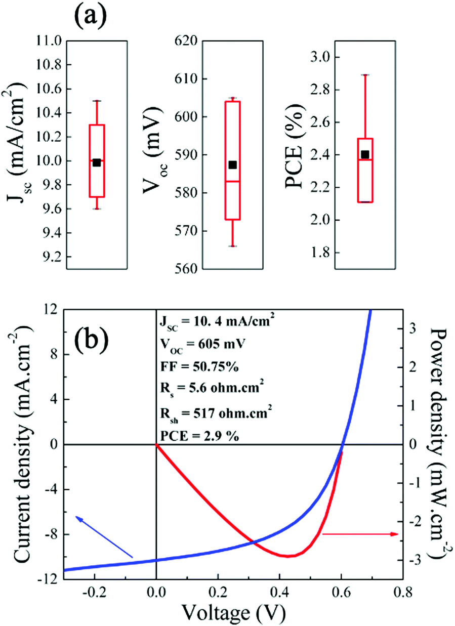 | ||
| Fig. 3 (a) Statistical distribution of JSC, VOC and PCE measured on nine 2.0 eV CIGS solar cells integrated on 1 FTO substrate. The black squares represent the average value of each parameter. (b) Current vs. voltage (blue line) and power vs. voltage (red line) characteristics of the champion solar cell. | ||
Solid-state properties of CdS/CIGS/FTO cells at cryogenic temperatures
 | ||
| Fig. 4 Temperature dependent current–voltage characteristics measured between 300 K and 150 K on (a) 1.2 eV CIGSe and (b) 2.0 eV CIGS solar cells. (c) Temperature dependence of series resistances measured under AM1.5G simulated illumination on CIGS (red circles) and CIGSe (blue squares) solar cells. | ||
The temperature-dependence of the CIGS solar cell electrical properties differs significantly from that of the CIGSe device (Fig. 4(b), refer to Table S3, ESI† for complete cell characteristics). A clear photocurrent suppression was observed with reduced temperatures, with JSC dropping from 9.37 mA cm−2 (300 K) to 4.49 mA cm−2 (150 K). Also, VOC was observed first to increase from 300 K (495 mV) to 200 K (640 mV) before decreasing at 150 K (602 mV). Finally, RS increases significantly as temperature is reduced, from 10.57 Ω cm2 at 300 K to 41.43 Ω cm2 at 150 K (Fig. 4(c)). For comparison, RS values measured on the CIGSe device increased only by 0.2 Ω cm2 in the same temperature range. We note that RSH measured on the CIGS solar cell were nearly constant between 300 K (202 Ω cm2) and 150 K (230 Ω cm2), yet about 5 times lower than those measured on CIGSe.
The electrical properties of the CIGS/FTO back contact were further investigated to clarify if the blocking diode model applies to this interface. For this analysis, the ITO/ZnO/CdS top layers of the CIGS cell were etched in a 10% HCl solution for 5 minutes and replaced by 100 nm-thick (area: 0.015 cm2) gold ohmic contacts58–60 evaporated directly onto the etched CIGS absorber. As presented in Fig. 5(a), all J–V–T characteristics measured in dark between 300 K and 140 K on Au/CIGS/FTO are linear and intersects the origin, revealing that an ohmic contact, rather than a blocking barrier, is formed at the CIGS/FTO back interface. However, a more rigorous analysis of the CIGS solar cell RS temperature dependence evidenced a barrier height ϕB against hole injection of about 30 meV at the CIGS/FTO interface (Fig. 6). Nonetheless, this value is too low to constitute a blocking barrier and have any significant impact on the cell's electrical properties.32 Additionally, one can rule out the contribution of the top transparent window layers and buffer, since RS measured on the CIGSe solar cell integrated with identical CdS, ZnO and ITO layers did not exhibit any temperature dependence (see Fig. 4(c)). Finally, the FTO in-plane resistance was measured in the same temperature range to evaluate its possible contribution to the CIGS solar cell RS. Here, two indium ohmic contacts (∼1 cm2), distant by ∼1.5 cm, were directly soldered onto a clean FTO substrate. As shown in Fig. 5(b), all J–V–T curves measured on the In/FTO/In stack exhibit an ohmic behavior and are virtually identical in the 300–140 K range. This demonstrates that the FTO back-contact resistance (as well as that of the In/FTO contacts) does not change with temperature and, as such, cannot be the origin of the CIGS solar cell RS temperature dependence.
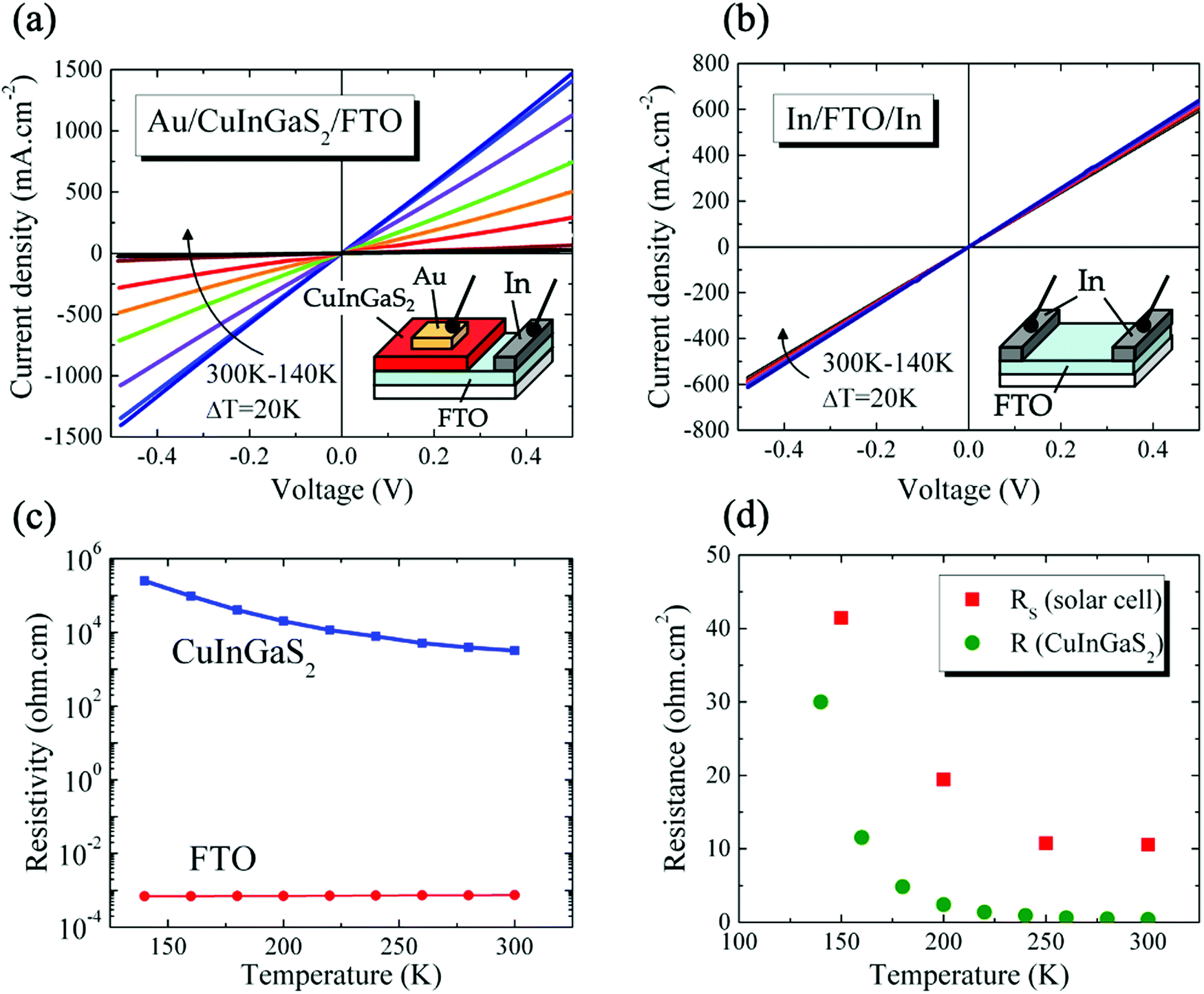 | ||
| Fig. 5 J–V characteristics measured in dark between 300 K and 140 K on (a) Au/CIGS/FTO and (b) In/FTO/In devices. Note that the contact area (A) and length (L) for each device differ significantly due to their unique geometry. For Au/CIGS/FTO, A = pad area = 0.015 cm2 and L = CIGS thickness = 1200 nm. For In/FTO/In, A = indium contact width × FTO thickness = 0.8 cm × 400 nm, and L = distance between pads = 1.5 cm. (c) Resistivity (Log scale) of CIGS and FTO as function of temperature calculated from J–V–T measurements shown in (a and b). (d) Comparison of the temperature dependence of CIGS resistance with that of CIGS solar cell series resistance. | ||
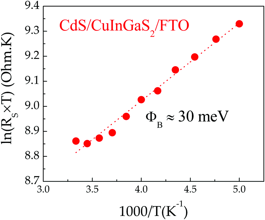 | ||
| Fig. 6 Arrhenius plot of Ln(Rs × T) derived from J–V–T measurements performed on CIGS solar cells between 200 K and 300 K. The barrier height ϕB at the CIGS/FTO interface is determined by fitting the plot to RS = (k/qA × T)exp(ϕB/kT), with A the effective Richardson constant. | ||
We conclude that the change in RS measured on the CIGS solar cell originates from the absorber itself. Fig. 5(c) presents the temperature-dependence of CIGS resistivity calculated using the J–V–T data measured on Au/CIGS/FTO (Fig. 5(a)). The absorber's resistivity increases by nearly two orders of magnitude between 300 K (3.2 × 10³ Ω cm) and 140 K (250 × 103 Ω cm). Comparatively, the resistivity of FTO, calculated from the J–V–T measured on the In/FTO/In stack (Fig. 5(c)), remained unchanged (7.4 × 10⁻⁴ Ω cm at 300 K; 6.9 × 10⁻⁴ Ω cm at 140 K). Also, we compare in Fig. 5(d) the temperature-dependence of RS to that of the CIGS resistance (calculated directly form the J–V–T data presented in Fig. 5(c)). The influence of the bulk resistance on the RS is clearly observed, with RS increase coinciding with that of CIGS resistance at temperatures below 250 K. Above this temperature, the contribution of CIGS is negligible and the solar cell RS is dominated by resistances outside of the junction (10.57 Ω cm2). These results suggest a carrier freeze-out mechanism with reducing temperature from larger ionization of the dominant acceptors in the absorber,61 as evidenced by the depth profiles of apparent doping density measured as function of temperature (75–300 K) and presented in Fig. S5 (ESI†). Unlike CIGSe, for which a constant NCV measured at 0 V was observed throughout the entire temperature range (∼5 × 1015 cm−3, Table S4, ESI†), a two-order of magnitude reduction in doping density was measured in CIGS (∼3 × 1017 cm−3 to ∼3 × 1015 cm−3, Table S4, ESI†). Other temperature-dependent contributions from non-ohmic barriers may be also present, such as between grains in the absorber layer57 or at the absorber-buffer interface as presented in the next section.
 | ||
| Fig. 7 Temperature dependent open circuit voltage measured between 300 K and 150 K on (a) 1.2 eV CIGSe and (b) 2.0 eV CIGS solar cells. | ||
Theoretical calculations were conducted to further understand the origin of this apparent FLP at the junction between CIGS and CdS. We first consider the influence of possible degradation of the CdS/CIGS interface in Fig. 8 through interfacial impurities, which summarizes the formation energies of incorporated Cd defects calculated in the parent compounds of CuInS2 and CuGaS2 in the Cu-poor growth conditions (Fig. 8(a)) most relevant to the synthesized 2.0 eV CIGS absorbers. For both CuInS2 and CuGaS2, we find that Cd may favorably incorporate on both the Cu site, acting as a shallow donor, and the group-III site, acting as an acceptor. Cadmium interstitials are predicted to be significantly higher in energy. Thus at the interface, Cd incorporation would be expected to lead to self-compensation that would pin the interfacial Fermi level near where the CdCu and CdIn concentrations are equivalent, assuming their concentration exceeds that of electrically-active native defects. This pinning level is shown as the dashed lines in Fig. 8(b and c), which we find to occur between ∼0.3–0.75 eV above the valence band maximum in CuInS2, and ∼0.75–1.2 eV in CuGaS2, for conditions spanning more S-rich/III-poor to S-poor/III-rich limits. Approximating this Fermi level window in the 2.0 eV band gap CIGS absorber from the 0.73 GGI-weighted average, this would suggest the interfacial Fermi level would be pinned within a window of 0.63–1.06 eV for Cu-poor conditions spanning the S-rich/III-poor to S-poor/III-rich limits. The entire range of interfacial Fermi-levels achievable is substantially lower than the band gap, with the lowest values predicted in the more Cu- and III-poor limit most consistent with the measured VSAT (636 meV). This suggests a severe detrimental impact to the achievable VOC with interfacial Cd incorporation in the sulfide absorbers.
 | ||
| Fig. 8 (a) Representative chalcopyrite phase diagram, calculated for CuGaS2 and shown as a function of the Ga and Cu chemical potentials (μ). The calculated formation energies of dilute Cd impurities are included for CuInS2 (b) and CuGaS2 (c), shown for conditions representing the regimes of Cu-poor and III-rich/S-poor and S-rich/III-poor limits, as also highlighted in (a). The Fermi level that would result from self-compensation from Cd incorporation is included as the dashed lines in (b and c). | ||
We also note that this same analysis performed for the CIGSe absorbers suggests an analogous pinning level of 0.56–0.90 eV for the Cu-poor and Se-rich/III-poor to Se-poor/III-rich limits that is essentially independent of the GGI (see Fig. S6 and Table S5, ESI†). This window of Fermi levels falls much closer to the band gaps and the measured VSAT (990 mV) in low-gap CIGSe absorbers supports the observation that the achievable VOC in CIGSe is robust to substantial interfacial Cd incorporation beyond the typical picture of CdCu donors incorporated onto vacant Cu sites during CdS deposition.
The nature of CBO at the buffer/absorber interface also plays a critical role in the device performance. Unlike CdS/CIGSe interfaces, for which small “spike-like”66 (<50 meV) or nearly flat67 CBO are generally observed, the “cliff-like”68 CBO brings EC in CdS closer to EV in CIGS and facilitates interface recombination. From calculated natural band alignments in ref. 69 and the analysis of the CIGS band edges with composition,30 we estimate a cliff-like CBO of ∼0.5–0.6 eV for 0.73 GGI CdS/CIGS heterojunction. If we also consider the possible formation of off-stoichiometric Cu-deficient phases, or ordered vacancy compounds (OVCs) in the sulfide interface, this can also influence the resulting band offsets with CdS. The OVC compounds tend to slightly increase the band gaps relative to the parent CIGSSe chalcopyrite phases in conjunction with an overall lowering of the band edge positions on an absolute energy scale, thus diminishing the expected cliff with CdS.70 Taking a GGI-weighted value for the CBO of the CuIn5S8 relative to CuInS2 (−0.42 eV) and CuGa5S8 relative to CuGaS2 (−0.79 eV),70 we obtain an estimated cliff-like CBO of −0.68 eV for a possible OVC alloy relative to the parent CIGS alloy. Taken with the CdS band edge positions, this would suggest the OVC formation would favorably improve the band alignment in the sulfide absorbers, leading to a significantly reduced cliff-like CBO of ∼0.1–0.2 eV. While this estimate assumes full miscibility in the OVC and no bowing effects, it gives a reasonable quantitative approximation for how these deficient phases would impact the overall band diagram of the device. Most importantly, it suggests that any OVCs, if present, would be beneficial from the standpoint of improving the band alignment of the sulfide absorber with the CdS buffer layer. With the current OVC-free CdS/CIGS interface, we estimate a CBO (∼EG–EA)71 of approx. 0.9 eV (Fig. 9), a value larger than the ∼0.6 eV determined from the theoretical natural band offsets that neglect potentially important interfacial details such as strain and local atomic structure. Nonetheless, the results support the poor conduction band alignment of CdS with 2.0 eV CIGS and emphasize the need for OVCs or EG-tunable buffers, such as MgxZn1−xO34 or Zn(O,S),72 to reduce interfacial CBO.
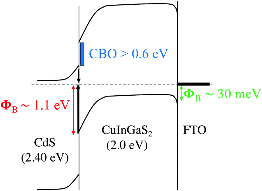 | ||
| Fig. 9 Tentative band diagram of the CdS/CIGS/FTO structure derived from solid-state measurements at cryogenic temperatures (not to scale). | ||
4. Conclusions
We have reported on the solid-state properties of 2.0 eV CIGS solar absorbers integrated on FTO substrates and interfaced with CdS buffer layers. In contrast with methods commonly reported for the synthesis of CIGS (sulfurization of Cu-rich metal stacks), our protocol permitted the fabrication of thin film absorbers with high optical transmittance for photons with energy lower than the bandgap (%TE<EG = 78%), an important attribute for tandem PV and PEC applications. The averaged short-circuit photocurrent density measured on 9 cells was 10.0 mA cm−2, a value corresponding to 70% of the optical limit for a 2.0 eV bandgap absorber. Also the quasi Fermi level splitting of 1.17 eV measured on the bare absorber corresponds to 70% of the maximal achievable value. However, PCE recorded were low (avg.: 2.4%) and, for the most part, hindered by modest VOC values (avg.: 587 mV). Subsequent analyses performed at low temperatures revealed significant photocurrent suppression, a behavior typically attributed to an energy barrier at the back contact. In the case of CIGS, we demonstrate that the photocurrent suppression originates from the absorber itself via early freeze-out of the dominant acceptors. Theoretical calculations suggest that Cd may favorably incorporate on both the Cu site, acting as a shallow donor, and the group-III site, acting an acceptor, leading to self-compensation that would pin the interfacial Fermi level. The resulting conduction band offset (∼0.9 eV) was found to be much higher than that typically reported for high efficiency devices (∼0–0.1 eV). Both FLP and the poor conduction band alignment of CdS with 2.0 eV CIGS emphasize the need for new OVCs or EG-tunable buffers in future chalcopyrite-based MJSC.Conflicts of interest
There are no conflicts to declare.Acknowledgements
This work was funded by the U.S. Department of Energy under contract DE-EE0008085. This work was authored in part by the National Renewable Energy Laboratory, operated by Alliance for Sustainable Energy, LLC, for the U.S. Department of Energy (DOE) under Contract No. DE-AC36-08GO28308. Funding provided by the U.S. Department of Energy, Office of Energy Efficiency and Renewable Energy, Hydrogen and Fuel Cell Technology Office. The views expressed in the article do not necessarily represent the views of the DOE or the U.S. Government. The U.S. Government retains and the publisher, by accepting the article for publication, acknowledges that the U.S. Government retains a nonexclusive, paid-up, irrevocable, worldwide license to publish or reproduce the published form of this work, or allow others to do so, for U.S. Government purposes.References
- J. F. Geisz, R. M. France, K. L. Schulte, M. A. Steiner, A. G. Norman, H. L. Guthrey, M. R. Young, T. Song and T. Moriarty, Nat. Energy, 2020, 5, 326–335 CrossRef CAS.
- J. Chen and C. E. Packard, Sol. Energy Mater. Sol. Cells, 2021, 225, 111018 CrossRef CAS.
- F. Dimroth, M. Grave, P. Beutel, U. Fiedeler, C. Karcher, T. N. D. Tibbits, E. Oliva, G. Siefer, M. Schachtner, A. Wekkeli, A. W. Bett, R. Krause, M. Piccin, N. Blanc, C. Drazek, E. Guiot, B. Ghyselen, T. Salvetat, A. Tauzin, T. Signamarcheix, A. Dobrich, T. Hannappel and K. Schwarzburg, Prog. Photovoltaics, 2014, 22, 277–282 CAS.
- S. Fan, Z. J. Yu, R. D. Hool, P. Dhingra, W. Weigand, M. Kim, E. D. Ratta, B. D. Li, Y. Sun, Z. C. Holman and M. L. Lee, Cell Rep. Phys. Sci., 2020, 1, 100208 CrossRef.
- W. Septina, C. P. Muzzillo, C. L. Perkins, A. C. Giovanelli, T. West, K. K. Ohtaki, H. A. Ishii, J. P. Bradley, K. Zhu and N. Gaillard, J. Mater. Chem. A, 2021, 9, 10419–10426 RSC.
- M. Nakamura, K. Yamaguchi, Y. Kimoto, Y. Yasaki, T. Kato and H. Sugimoto, IEEE, 2019, 9, 1863–1867 Search PubMed.
- D. H. Kim, C. P. Muzzillo, J. Tong, A. F. Palmstrom, B. W. Larson, C. Choi, S. P. Harvey, S. Glynn, J. B. Whitaker, F. Zhang, Z. Li, H. Lu, M. F. A. M. van Hest, J. J. Berry, L. M. Mansfield, Y. Huang, Y. Yan and K. Zhu, Joule, 2019, 3, 1734–1745 CrossRef CAS.
- J. H. Wi, W. S. Han, W. J. Lee, D. H. Cho, H. J. Yu, C. W. Kim, C. Jeong, J. H. Yun, C.-I. Il Kim and Y. D. Chung, IEEE J. Photovoltaics, 2018, 8, 840–848 Search PubMed.
- S. Kijima and T. Nakada, Appl. Phys. Express, 2008, 1, 0750021 Search PubMed.
- F. Larsson, N. S. Nilsson, J. Keller, C. Frisk, V. Kosyak, M. Edoff and T. Törndahl, Prog. Photovoltaics, 2017, 25, 755–763 CAS.
- D. L. Young, J. Keane, A. Duda, J. A. M. AbuShama, C. L. Perkins, M. Romero and R. Noufi, Prog. Photovoltaics, 2003, 11, 535–541 CAS.
- M. A. Contreras, L. M. Mansfield, B. Egaas, J. Li, M. Romero, R. Noufi, E. Rudiger-Voigt and W. Mannstadt, 2011 37th IEEE Photovoltaic Specialists Conference, IEEE, 2011, vol. 1, pp. 000026–000031.
- T. Nakada, Y. Hirabayashi, T. Tokado, D. Ohmori and T. Mise, Sol. Energy, 2004, 77, 739–747 CrossRef CAS.
- B. Marsen, B. Cole and E. L. Miller, Sol. Energy Mater. Sol. Cells, 2008, 92, 1054–1058 CrossRef CAS.
- N. Gaillard, D. Prasher, J. Kaneshiro, S. Mallory and M. Chong, Mater. Res. Soc. Symp. Proc., 2013, 1558, mrss13-1558-z02-07 CrossRef.
- J. Kim, T. Minegishi, J. Kobota and K. Domen, Energy Environ. Sci., 2012, 5, 6368–6374 RSC.
- D. Yokoyama, T. Minegishi, K. Maeda, M. Katayama, J. Kubota, A. Yamada, M. Konagai and K. Domen, Electrochem. Commun., 2010, 12, 851–853 CrossRef CAS.
- T. J. Jacobsson, V. Fjällström, M. Sahlberg, M. Edoff and T. Edvinsson, Energy Environ. Sci., 2013, 6, 3676 RSC.
- M. G. Kibria, F. A. Chowdhury, S. Zhao, B. AlOtaibi, M. L. Trudeau, H. Guo and Z. Mi, Nat. Commun., 2015, 6, 1–8 Search PubMed.
- Y. Goto, T. Hisatomi, Q. Wang, T. Higashi, K. Ishikiriyama, T. Maeda, Y. Sakata, S. Okunaka, H. Tokudome, M. Katayama, S. Akiyama, H. Nishiyama, Y. Inoue, T. Takewaki, T. Setoyama, T. Minegishi, T. Takata, T. Yamada and K. Domen, Joule, 2018, 2, 509–520 CrossRef CAS.
- A. Fujishima and K. Honda, Nature, 1972, 238, 37–38 CrossRef CAS PubMed.
- J. L. Young, M. A. Steiner, H. Döscher, R. M. France, J. A. Turner and T. G. Deutsch, Nat. Energy, 2017, 2, 17028 CrossRef CAS.
- P. Varadhan, H. C. Fu, Y. C. Kao, R. H. Horng and J. H. He, Nat. Commun., 2019, 10, 1–9 CrossRef CAS PubMed.
- A. Nakamura, Y. Ota, K. Koike, Y. Hidaka, K. Nishioka, M. Sugiyama and K. Fujii, Appl. Phys. Express, 2015, 8, 107101 CrossRef.
- J. Jia, L. C. Seitz, J. D. Benck, Y. Huo, Y. Chen, J. W. D. Ng, T. Bilir, J. S. Harris and T. F. Jaramillo, Nat. Commun., 2016, 7, 1–6 Search PubMed.
- C. P. Muzzillo, W. E. Klein, Z. Li, A. D. Deangelis, K. Horsley, K. Zhu and N. Gaillard, ACS Appl. Mater. Interfaces, 2018, 10, 19573–19579 CrossRef CAS.
- M. Moriya, T. Minegishi, H. Kumagai, M. Katayama, J. Kubota and K. Domen, J. Am. Chem. Soc., 2013, 135, 3733–3735 CrossRef CAS PubMed.
- L. C. Seitz, Z. Chen, A. J. Forman, B. A. Pinaud, J. D. Benck and T. F. Jaramillo, ChemSusChem, 2014, 7, 1372–1385 CrossRef CAS PubMed.
- A. D. Deangelis, K. Horsley and N. Gaillard, J. Phys. Chem. C, 2018, 122, 14304–14312 CrossRef CAS.
- N. Gaillard, D. Prasher, M. Chong, A. Deangelis, K. Horsley, H. A. Ishii, J. P. Bradley, J. Varley and T. Ogitsu, ACS Appl. Energy Mater., 2019, 2, 5515–5524 CrossRef CAS.
- N. Gaillard and A. Deangelis, in Solar to Chemical Energy Conversion: Theory and Application, ed. M. Sugiyama, K. Fujii and S. Nakamura, Springer International Publishing, Cham, 2016, pp. 261–279 Search PubMed.
- A. Redinger, M. Mousel, M. H. Wolter, N. Valle and S. Siebentritt, Thin Solid Films, 2013, vol. 535, pp. 291–295 Search PubMed.
- D. B. Mitzi, O. Gunawan, T. K. Todorov and D. A. R. Barkhouse, Philos. Trans. R. Soc., A, 2013, 371, 20110432 CrossRef PubMed.
- I. S. Khan, C. P. Muzzillo, C. L. Perkins, A. G. Norman, J. L. Young, N. Gaillard and A. Zakutayev, J. Phys. Energy, 2021, 3, 024001 CrossRef CAS.
- J. Heyd, G. E. Scuseria and M. Ernzerhof, J. Chem. Phys., 2003, 118, 8207–8215 CrossRef CAS.
- G. Kresse and J. Furthmüller, Phys. Rev. B: Condens. Matter Mater. Phys., 1996, 54, 11169–11186 CrossRef CAS.
- G. Kresse and J. Furthmüller, Comput. Mater. Sci., 1996, 6, 15–50 CrossRef CAS.
- C. Freysoldt, B. Grabowski, T. Hickel, J. Neugebauer, G. Kresse, A. Janotti and C. G. Van de Walle, Rev. Mod. Phys., 2014, 86, 253–305 CrossRef.
- C. Freysoldt, J. Neugebauer and C. G. Van de Walle, Phys. Rev. Lett., 2009, 102, 16402 CrossRef.
- P. Jackson, R. Würz, U. Rau, J. Mattheis, M. Kurth, T. Schlötzer, G. Bilger and J. H. Werner, Prog. Photovoltaics, 2007, 15, 507–519 CAS.
- M. Bär, W. Bohne, J. Röhrich, E. Strub, S. Lindner, M. C. Lux-Steiner, C.-H. Fischer, T. P. Niesen and F. Karg, J. Appl. Phys., 2004, 96, 3857–3860 CrossRef.
- N. Gaillard, Wide Band Gap Chalcopyrite Photoelectrodes for Direct Water Splitting - Final report to the U.S. Department of Energy (EE0006670), Golden, CO (United States), 2019 Search PubMed.
- A. Lomuscio, T. Rödel, T. Schwarz, B. Gault, M. Melchiorre, D. Raabe and S. Siebentritt, Phys. Rev. Appl., 2019, 11, 1 Search PubMed.
- P. Wurfel, J. Phys. C: Solid State Phys., 1982, 15, 3967–3985 CrossRef.
- T. Kirchartz and U. Rau, Adv. Energy Mater., 2018, 8, 1703385 CrossRef.
- A. Polman, M. Knight, E. C. Garnett, B. Ehrler and W. C. Sinke, Science, 2016, 352, aad4424 CrossRef PubMed.
- F. Babbe, L. Choubrac and S. Siebentritt, Sol. RRL, 2018, 2, pp. 1–6 Search PubMed.
- D. B. Mitzi, O. Gunawan, T. K. Todorov, K. Wang and S. Guha, Sol. Energy Mater. Sol. Cells, 2011, 95, 1421–1436 CrossRef CAS.
- S. Merdes, R. Mainz, J. Klaer, A. Meeder, H. Rodriguez-Alvarez, H. W. Schock, M. C. Lux-Steiner and R. Klenk, Sol. Energy Mater. Sol. Cells, 2011, 95, 864–869 CrossRef CAS.
- R. Klenk, J. Klaer, R. Scheer, M. C. Lux-Steiner, I. Luck, N. Meyer and U. Rühle, Thin Solid Films, 2005, 480–481, 509–514 CrossRef CAS.
- Q. Cao, O. Gunawan, M. Copel, K. B. Reuter, S. J. Chey, V. R. Deline and D. B. Mitzi, Adv. Energy Mater., 2011, 1, 845–853 CrossRef CAS.
- A. O. Pudov, A. Kanevce, H. A. Al-Thani, J. R. Sites and F. S. Hasoon, J. Appl. Phys., 2005, 97, 064901 CrossRef.
- M. Burgelman, F. Engelhardt, J. F. Guillemoles, R. Herberholz, M. Igalson, R. Klenk, M. Lampert, T. Meyer, V. Nadenau, A. Niemegeers, J. Parisi, U. Rau, H.-W. Schock, M. Schmitt, O. Seifert, T. Walter and S. Zott, Prog. Photovoltaics, 1997, 5, 121–130 CAS.
- J. B. Varley and V. Lordi, J. Appl. Phys., 2014, 116, 63505 CrossRef.
- J. B. Varley, V. Lordi, X. He and A. Rockett, J. Appl. Phys., 2016, 119, 25703 CrossRef.
- T. Eisenbarth, T. Unold, R. Caballero, C. A. Kaufmann and H.-W. Schock, J. Appl. Phys., 2010, 107, 034509 CrossRef.
- O. Gunawan, T. K. Todorov and D. B. Mitzi, Appl. Phys. Lett., 2010, 97, 233506 CrossRef.
- P. J. Rostan, J. Mattheis, G. Bilger, U. Rau and J. H. Werner, Thin Solid Films, 2005, 480–481, 67–70 CrossRef CAS.
- N. Neugebohrn, M. S. Hammer, J. Neerken, J. Parisi and I. Riedel, Thin Solid Films, 2015, 582, 332–335 CrossRef CAS.
- T. Nakada, Y. Hirabayashi and T. Tokado, Jpn. J. Appl. Phys., 2002, 41, L1209–L1211 CrossRef CAS.
- O. Gunawan, T. K. Todorov and D. B. Mitzi, Appl. Phys. Lett., 2010, 97, 233506 CrossRef.
- V. Nadenau, U. Rau, A. Jasenek and H. Schock, J. Appl. Phys., 2000, 87, 584 CrossRef CAS.
- C. P. Thompson, S. Hegedus, W. Shafarman and D. Desai, 33rd IEEE Photovolt. Spec. Conf., 2008, 1–6 CAS.
- S. Shukla, D. Adeleye, M. Sood, F. Ehre, A. Lomuscio, T. P. Weiss, D. Siopa, M. Melchiorre and S. Siebentritt, Phys. Rev. Mater., 2021, 5, 055403 CrossRef CAS.
- J. D. Cohen, Identifying the Electronic Properties Relevant to Improving the Performance of High Band-Gap Copper Based I-III-VI2 Chalcopyrite Thin Film Photovoltaic Devices: Final Subcontract Report -NREL/SR-520-43909, 2007 Search PubMed.
- D. Hauschild, D. Kreikemeyer-Lorenzo, P. Jackson, T. M. Friedlmeier, D. Hariskos, F. Reinert, M. Powalla, C. Heske and L. Weinhardt, ACS Energy Lett., 2017, 2, 2383–2387 CrossRef CAS.
- M. Morkel, L. Weinhardt, B. Lohmüller, C. Heske, E. Umbach, W. Riedl, S. Zweigart and F. Karg, Appl. Phys. Lett., 2001, 79, 4482–4484 CrossRef CAS.
- L. Weinhardt, O. Fuchs, D. Groß, G. Storch, E. Umbach, N. G. Dhere, A. A. Kadam, S. S. Kulkarni and C. Heske, Appl. Phys. Lett., 2005, 86, 1–3 CrossRef.
- J. B. Varley, V. Lordi, T. Ogitsu, A. Deangelis, K. Horsley and N. Gaillard, J. Appl. Phys., 2018, 123, 161408 CrossRef.
- A. Sharan, F. P. Sabino, A. Janotti, N. Gaillard, T. Ogitsu and J. B. Varley, J. Appl. Phys., 2020, 127, 065303 CrossRef CAS.
- M. Turcu, O. Pakma and U. Rau, Appl. Phys. Lett., 2002, 80, 2598–2600 CrossRef CAS.
- S. Shukla, M. Sood, D. Adeleye, S. Peedle, G. Kusch, D. Dahliah, M. Melchiorre, G.-M. Rignanese, G. Hautier, R. Oliver and S. Siebentritt, Joule, 2021, 5, 1816–1831 CrossRef CAS.
Footnote |
| † Electronic supplementary information (ESI) available. See DOI: 10.1039/d1ma00570g |
| This journal is © The Royal Society of Chemistry 2021 |