
 Open Access Article
 This Open Access Article is licensed under a Creative Commons Attribution-Non Commercial 3.0 Unported Licence
Mapping the nanoscale effects of charge traps on electrical transport in grain structures of indium tin oxide thin films†
Hyesong
Jeon
 a,
Jeongsu
Kim
b,
Shashank
Shekhar
b,
Jeehye
Park
b and
Seunghun
Hong
*b
a,
Jeongsu
Kim
b,
Shashank
Shekhar
b,
Jeehye
Park
b and
Seunghun
Hong
*b
aDepartment of Materials Science and Engineering, Seoul National University, Seoul 08826, Korea
bDepartment of Physics and Astronomy, Institute of Applied Physics, Seoul National University, Seoul 08826, Korea. E-mail: seunghun@snu.ac.kr
First published on 14th July 2021
Abstract
We report the mapping of the nanoscale effects of charge trap activities in the grain structures of an oxygen plasma-treated indium tin oxide (ITO) thin film. Here, a conducting Pt probe made direct contact with the surface of an ITO thin film and scanned the surface while measuring the maps of electrical currents and noises. The measured data were analyzed to obtain the maps of sheet conductance (Gs) and charge trap density (Neff) in the grain structures of the ITO thin film. The results showed that grain boundaries exhibited a lower sheet conductance and a higher charge trap density than those of the regions inside grains. Interestingly, the scaling behavior of Gs ∝ Neff−0.5 was observed in both grain and boundary regions, indicating diffusive charge transport. Furthermore, the sheet conductance increased by two times, and the density of charge traps decreased by ∼70% after an oxygen plasma treatment, presumably due to the enhanced crystallinity of the ITO film. Interestingly, in some boundary regions, the sheet conductance and the charge trap density exhibited the scaling behavior of Gs ∝ Neff0.5, which was attributed to the hopping conduction caused by the enhanced crystallinity and increased localized states in the boundary regions. Since our method provides valuable insights into charge transport and charge trap activities in transparent conducting thin films, it can be a powerful tool for basic research and practical optoelectronic device applications based on ITO thin films.
1. Introduction
Indium tin oxide (ITO) is a highly n-doped semiconductor with a low resistivity of ∼10−4 Ω cm, a high carrier mobility of ∼1–10 cm2 V−1 s−1, and a high carrier concentration of 1020–1021 cm−3.1,2 Furthermore, an ITO thin film shows high optical transmittance (∼80%)3 in visible and NIR regions, which originates from a wide band gap of ∼3.5–4.3 eV.4 Since ITO thin films have remarkable electrical and optical properties, they have been extensively utilized as transparent conducting electrodes for various optoelectronic devices such as light-emitting diodes (LEDs), organic photovoltaics (OPVs), solar cells, and touch screen displays.3,5–9The electrical properties of an ITO thin film depend on different deposition conditions and post-treatments.4,10–18 For example, an oxygen plasma treatment is commonly used to improve the conductivity and uniformity of ITO films.6,10,19 And, such an improvement after the plasma treatment has often been attributed to different activities of charge traps in ITO thin films.5,6,19–22 However, since charge traps can also generate current noises, extensive efforts have been made to understand the effect of charge traps in ITO films. A common method to study charge trap activities is the measurement of noise spectra in an ITO channel using a spectrum analyzer, which provides versatile information about the frequency-dependent properties of charge trap activities. However, it has been very difficult to directly map the activities of such charge traps in ITO films at a nanoscale resolution. Previous reports say that it has been very challenging to perform defect analyses through elemental mapping or electron microscopies at a nanoscale resolution.23 Recently, we reported a scanning noise microscopy method that allows one to map the activities of electrical noise sources in lateral and vertical electrical channels at a nanoscale resolution.20,24,25 In the conducting film, lateral transport is the dominant conduction mechanism between the electrodes.25 However, such a method has not been utilized for ITO films.
Herein, we mapped the nanoscale effects of charge trap activities on charge carrier transport in oxygen plasma-treated ITO thin films. In this work, the maps of electrical currents and noises were recorded using a conducting probe in contact with an ITO thin film. By analysing the measured data, we could obtain the maps of sheet conductance and localized charge trap distributions in the ITO thin film with a nanoscale resolution. These maps show a lower sheet conductance and a higher density of charge traps in grain boundaries than those inside the grains. Interestingly, the sheet conductance and the charge trap density had the scaling behaviour of Gs ∝ Neff−0.5, indicating diffusive charge transport in the ITO thin film. Additionally, we observed an increased sheet conductance and a decreased charge trap density in the ITO thin film after an oxygen plasma treatment. Furthermore, some of the grain boundary regions exhibited an interesting scaling relation of Gs ∝ Neff0.5, which was attributed to the hopping conductivity through the localized states in the band gap. 2D materials such as graphene, reduced graphene oxide (RGO), and MoS2 do not exhibit much variation in sheet conductance within a domain or grain.20,24,25 Since our method provides valuable insights into the nanoscale charge transport and charge trap activities in ITO thin films, it can be a useful tool for the basic research and development of optoelectronic devices based on ITO.
2. Experimental section
2.1 Sample preparation
An ITO thin film on a glass substrate was purchased from Sigma Aldrich, Inc. (product ID 703192). The ITO thin film was rinsed successively with acetone, ethanol, and deionized water for 1 min each and dried with nitrogen blowing. Then, a Ti/Au electrode (10/30 nm thickness) was deposited in an area of ∼0.2 × 1.2 cm2 onto the ITO thin film using a thermal evaporator with a shadow mask.For the oxygen plasma treatment, an ITO thin film was exposed to the oxygen plasma produced by a radio frequency (RF) plasma generator (PDC-002, Harrick Plasma). We applied a RF power of 30 W for 5 min with an oxygen pressure of ∼100 mTorr.
2.2 Electrode fabrication for electrical measurements
To evaluate the basic characteristics of a bulk ITO film, two Ti/Au electrodes (10/30 nm, the size of ∼0.2 × 1.2 cm2) separated by 1.2 cm were first deposited on the ITO film sample through a shadow mask using thermal evaporation. And, electrical measurements were performed between the electrodes.2.3 Experimental set-up for noise measurements
Fig. 1 shows the scanning noise microscopy set-up for our current and noise measurements. Here, a conducting Pt probe (25Pt300B, Park Systems Inc.) installed in a conducting atomic force microscope (c-AFM) (XE-70, Park Systems Inc.) made direct contact with the surface of an ITO thin film. The contact force between the conducting Pt probe and the ITO surface was maintained at 2 μN, and a DC bias voltage of 0.06 V was applied to the Ti/Au electrode using a function generator (DS345, Standard Research Systems). Here, the current signals through the Pt probe were measured and converted to voltage signals by a low-noise preamplifier (SR570, Stanford Research Systems). Simultaneously, noise signals (the fluctuating component of an electrical current signal) were collected through a band-pass filter (6 dB) in the preamplifier (SR570, Stanford Research Systems), and the RMS power of the measured noise signals was obtained using a homemade RMS-to-DC converter. The measured RMS noise power was divided by the bandwidth of the band-pass filter to estimate the absolute noise power spectral density (PSD). By scanning the probe on an ITO surface, high-resolution topography, current, and noise PSD maps could be acquired simultaneously. The measured maps were analysed using a numerical method to obtain the maps of sheet conductance and charge trap density. It is worth mentioning that, in this work, we mapped ITO on an insulating glass substrate because ITO has often been utilized as a transparent electrode on insulating substrates. However, we could also map ITO films on conducting substrates to analyse the vertical conduction through the ITO film like other electronic materials reported previously.22,26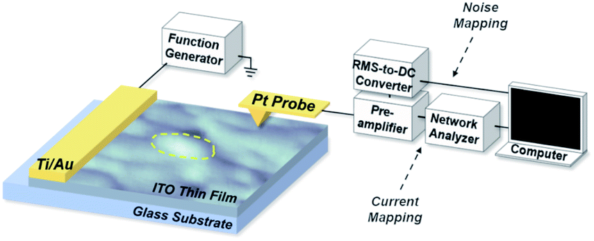 | ||
| Fig. 1 Schematic diagram depicting a scanning noise microscopy set-up for an ITO thin film on a glass substrate. The enclosed area in the yellow dashed line indicates a grain in the ITO thin film. A conducting Pt probe installed on a conducting AFM made contact with the surface of the ITO thin film and scanned over the surface during the measurement. Electrical current and noise maps were measured simultaneously and analysed to obtain sheet conductance and charge trap density maps. | ||
3. Results and discussion
3.1 Basic characteristics of bulk ITO thin films
Fig. 2a shows the transmittance curve of a bulk ITO thin film in the UV-visible range. We measured an optical transmittance using a UV-vis/NIR spectrophotometer (V-770, JASCO). The result shows that the ITO thin film has a high optical transmittance of over ∼80%. Also, note that the transmittance decreased below the ∼350 nm wavelength, indicating its bandgap of ∼3.5 eV as reported previously.4,27,28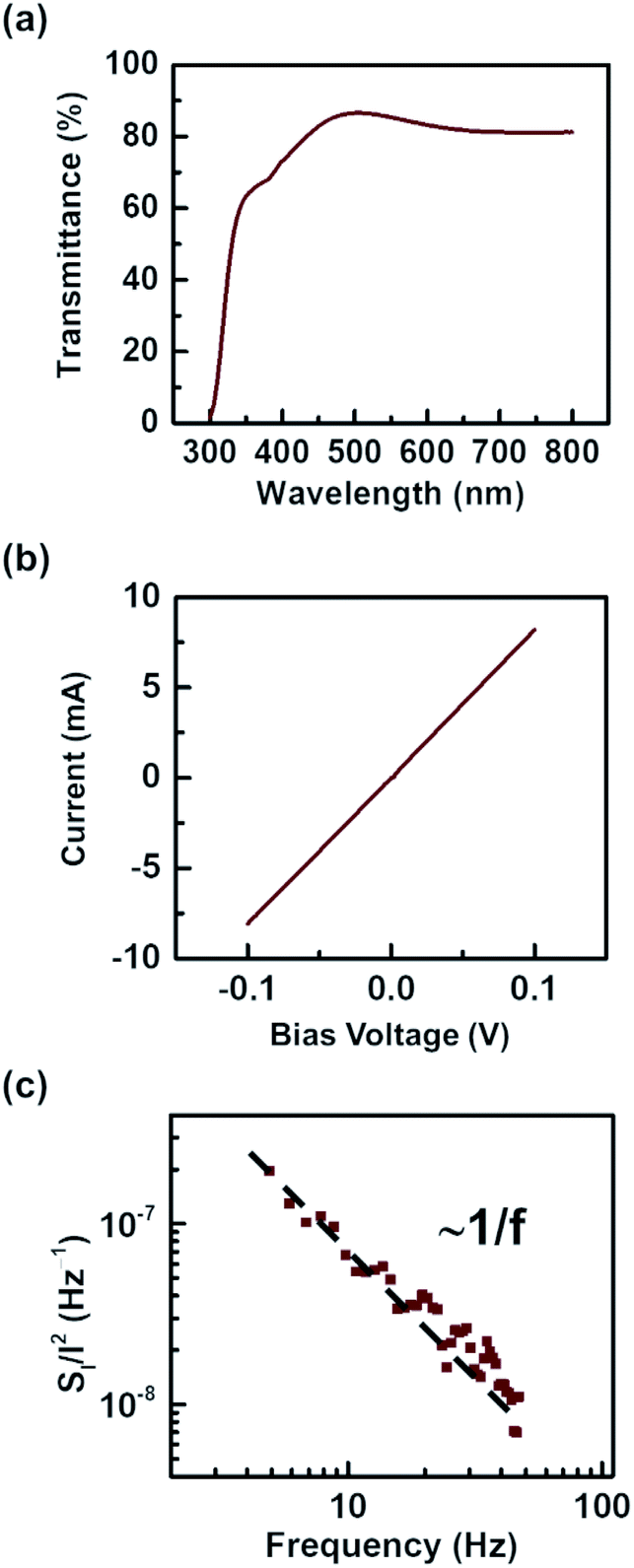 | ||
| Fig. 2 Basic characterization of an ITO thin film. (a) Transmittance spectrum of the ITO thin film. (b) Current–voltage curve measured on the ITO film. (c) Current-normalized noise PSD (SI/I2) dependence on frequencies. The 1/f noise behavior was observed in the frequency range of 4–50 Hz. | ||
To analyse the basic electrical characteristics of ITO films used in our experiments, a current–voltage (I–V) curve of a bulk ITO thin film between two electrodes was measured using a Keithley 4200-SCS semiconductor parameter analyser (Fig. 2b). Here, the length and the width of the ITO channel were 1.2 cm and 1.2 cm, respectively. Its thickness was ∼150 nm. The measured currents were linearly proportional to the applied bias, indicating good ohmic contact between the ITO channel and the electrode. From the slope of the I–V curve and the dimensions of the ITO channel, we could estimate its conductivity value of ∼5.1 × 10⁴ S m−1, which is consistent with the previously reported value (∼104 S m−1) for a similar thickness.29
Fig. 2c is the frequency dependence of a current-normalized noise PSD (SI/I2) spectrum on a log–log scale, which is measured from the same bulk ITO film as in Fig. 2b. A fast Fourier transform (FFT) network analyzer (SR770, Standard Research Systems) with a bias voltage of 0.1 V was utilized to measure a noise power spectrum in a frequency range from 5 to 50 Hz. Note that SI/I2 shows a typical 1/f behavior. In previous studies, it was reported that when electrical noises were generated by a small number of trap states with a similar trapping time, a noise PSD spectrum exhibited a scaling behavior of ∼1/f2.20–22 On the other hand, in the case of numerous trap states with random trapping time, a noise spectrum usually shows ∼1/f behavior.20–22 Our results with ∼1/f behavior indicate that there were numerous trap states with different trapping times in our bulk ITO samples, as reported previously.30
3.2 Nanoscale mapping of charge trap activities
The scanning noise microscopy set-up shown in Fig. 1 was utilized to analyse the charge trap activities in the ITO thin film with a nanoscale resolution (Fig. 3). Fig. 3a shows the AFM topography image of an untreated ITO thin film on a glass substrate. The topography map shows multiple grain structures whose sizes ranged from 100 to 200 nm, consistent with previously reported studies.17,18 The surface roughness was ∼4 nm. It should be mentioned that the map shows some topological variations like gaps and holes. However, since they have a rather small aspect ratio due to a small depth (<2 nm) and large dimensions (>20 nm), we can expect that the probe can maintain reliable contact on the surface and the effect of topological variations on electrical measurements should be minimal. A boundary of a typical grain was marked by a yellow dashed line. Previous studies showed that such grain structures were due to grain growth during a film deposition process.13,17 The sizes of grains are known to vary depending on different parameters such as the deposition method, growth conditions, and the post-treatment on an ITO thin film.13,16–18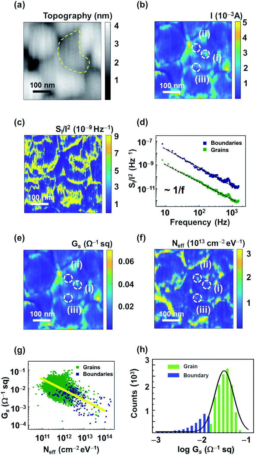 | ||
| Fig. 3 Nanoscale sheet-conductance and charge trap density mapping of ITO thin films. (a) AFM topography image of the ITO thin film. The film was comprised of grains distinguished by grain boundaries (marked by a yellow dashed line). (b) Current (I) map of the film. Marks of (i) and (ii) represent the regions in a grain, and mark (iii) represents a grain boundary. The bias voltage of 0.06 V was applied to the film through a metal electrode for measurements. (c) Current-normalized noise PSD (SI/I2) map of the film at a central frequency of 17.32 Hz. (d) Current-normalized noise PSD (SI/I2) dependence on frequencies at each of the grains and grain boundaries. (e) Sheet conductance (Gs) map for the ITO film. (f) Charge trap density (Neff) map for the film. (g) Scattered plot showing the relationships between the Gs and Neff. The slope of a fitting line (yellow-colored) is ∼−0.5. (h) Histograms showing the statistical distribution of sheet conductance values in the grains and boundaries of the Gs maps in (e). | ||
Fig. 3b and c are the maps of electrical current (I) and current-normalized noise PSD (SI/I2) measured on the ITO thin film, respectively. Here, a DC bias voltage of 0.06 V was applied to a Ti/Au electrode, and the electrical currents through the Pt tip were measured while the tip is scanning on the ITO surface (Fig. 1). The noise PSD (SI) map (at 17.32 Hz) was measured simultaneously with the current map. The measured SI map was divided by the square of the current map to obtain the map of normalized noise PSD SI/I2. The results show that grain boundaries (marked by (iii) in Fig. 3b) had lower currents and higher noise levels than those inside grain regions (marked by (i) and (ii) in Fig. 3b). Previous work showed that grain boundaries usually have a rather large number of defects, and they could act as barriers blocking carrier transport which is somewhat consistent with our results.22,31 Also, note that even inside the grain, currents and noises varied depending on the locations, presumably due to the non-uniform distribution of defects inside the grain.5,20,30,32
Fig. 3d shows the frequency dependence of the current-normalized noise PSD (SI/I2) which was measured at a fixed location in the grain or boundary regions. Here, a Pt probe installed on a c-AFM was placed on a fixed location of the grain (marked by (i) in Fig. 3b) or grain boundary (marked by (iii) in Fig. 3b), and noise spectra were measured in the frequency range of 1 Hz to 1.56 kHz using a fast Fourier transform (FFT) network analyzer (SR770, Standard Research Systems). During the measurement, a DC bias voltage of 0.06 V was applied to the Ti/Au electrode. The data can be fitted by a 1/f graph as shown by solid lines. We actually observed a similar 1/f behavior for all of our ITO samples, indicating numerous charge traps with different trapping times in both grains and boundaries.20,24 Also, note that the SI/I2 values of grain boundaries were higher than those inside grains at the same frequency. It indicates that larger electrical noises were generated in grain boundaries than those inside the grains of the ITO thin film, which is consistent with the measured SI/I2 map (Fig. 3c).
Fig. 3e shows the sheet conductance (Gs) map, which was estimated from the current map in Fig. 3b. To obtain the sheet resistance map, we used a computational iterative method developed in our previous work.24 The details of the computation method are provided in the ESI (Fig. S1†). In brief, the sheet resistance map was calculated from the current map of the ITO thin film using the recursive computational secant-algorithm. Then, the sheet conductance map was obtained by taking the reciprocal of the sheet resistance map. The Gs values in the grain (marked by (i)) and grain boundary (marked by (iii)) were ∼3.9 × 10⁻² Ω−1 sq and ∼6.4 × 10⁻³ Ω−1 sq, respectively. The result indicates that the boundary had about six times lower values than the region inside the grain. The result was consistent with the sheet conductance values measured on a bulk ITO thin film (∼10−2 Ω−1 sq) in Fig. 2b. Previous work showed that grain boundaries have intergranular amorphous phases with a large number of defects and lattice mismatches. Such a large number of defects in grain boundaries may lead to increased carrier scattering and eventually obstruct the carrier flow in an ITO thin film.4,33 The rather low sheet conductance values of the boundary regions could be attributed to the increased number of scattering centers in the boundary regions.4,33 Also, the sheet conductance map shows that there was a significant variation of sheet conductance values even inside the grain regions like ∼9.3 × 10⁻³ Ω−1 sq (marked by (ii)) and ∼3.9 × 10⁻² Ω−1 sq (marked by (i)), indicating that the conductance in region (i) is 4.2 times larger than that in region (ii). Previous work showed that defects often act as charge traps for free carriers, generating electrical noises.5,20,30,32 The rather large variation of conductance inside the grain regions can be attributed to the inhomogeneous distribution of defects in crystalline grains. Such a variation of conductance values in ITO films has been predicted theoretically, but it has been challenging to map it directly. Since our method allows one to directly map the conductance variations in both grain and boundary regions, it should be a powerful tool for basic research and the development of practical devices.
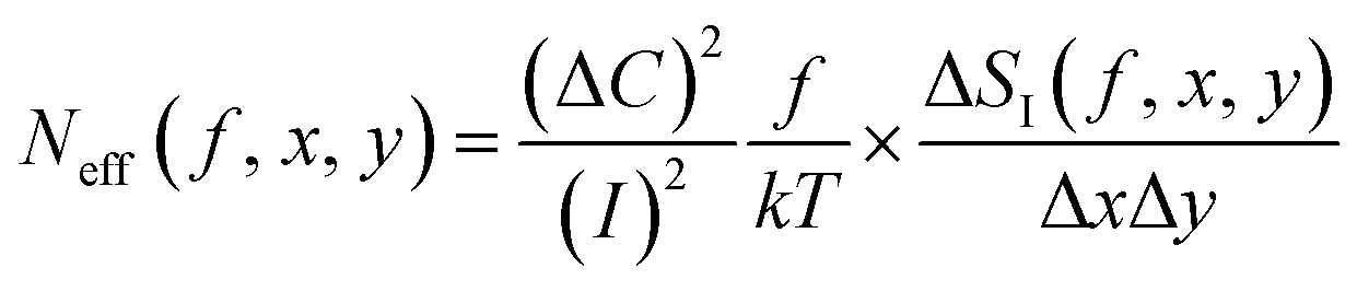
The effective charge trap density (Neff) map of an ITO thin film was estimated from the current and noise maps using a resistance network model as formulated previously (Fig. 3f).20,21,24 The details are provided in the description of Fig. S2 in the ESI.† In brief, we modeled the ITO film as a two-dimensional network of resistances corresponding to those between small ITO segments on an x–y plane (Fig. S1, ESI†). Based on the model, we can estimate the Neff in a small area ΔxΔy at (x, y) on an ITO thin film as follows
 | (1) |
Fig. 3g is a scatter plot showing a relation between the sheet conductance (Gs) and the charge trap density (Neff) of grains and grain boundaries in the ITO thin film on a log–log scale. The data points for grains and boundaries were denoted by green and blue squares, respectively. Each data point was obtained from the same location in the Gs map and the corresponding Neff map (Fig. 3e and f). The plot shows that boundaries have smaller values of Gs and higher values of Neff than the regions inside grains. Interestingly, we observed that the Gs was inversely proportional to the square root of the Neff as expressed below:
| Gs ∝ N−0.5eff | (2) |
As reported previously, it is the typical behavior of diffusive charge transport where charge carriers are scattered by multiple scattering centers such as charge traps and lattice disorderings.20,25 Presumably, the charge traps in an ITO thin film can obstruct the transport of charge carriers, resulting in a rather low sheet conductance. This result implies that charge trap density can be one of the main factors determining the sheet conductance of an ITO thin film.
For a further analysis of the conductance distribution in Fig. 3c, we plotted the histograms of sheet conductance (Gs) in the regions of grains and boundaries with green and blue color, respectively (Fig. 3h). The histogram of Neff is also provided in the ESI (Fig. S3a†). Note that the boundary regions exhibited a rather low sheet conductance and a large noise source density. A plausible explanation can be that the defects in the boundary regions increased the scattering during charge carrier transport, and some of them worked as charge traps generating current noises.22,25,29 It should also be noted that the histograms can be fitted with a Gaussian (normal) distribution with an x-axis on a log scale, indicating log-normal distributions. Previous studies showed that such a log-normal distribution of sheet conductance values is a typical characteristic of percolative networks in the film.21,42 Presumably, in our ITO films, individual grains are somewhat separated by rather resistive grain boundaries, thus exhibiting characteristic behavior of percolative networks.
3.3 Oxygen plasma treatment effects on ITO thin films
We also investigated the effect of oxygen plasma treatment on ITO thin films (Fig. 4). Fig. 4a shows the sheet conductance (Gs) map of an oxygen plasma-treated ITO thin film. Here, an oxygen plasma treatment was applied to an ITO thin film using a RF plasma generator with a RF power of 30 Watt and an oxygen pressure of ∼100 mTorr for 5 min. The Gs value on the grain boundary (marked by (iii)) was ∼8.4 × 10⁻³ Ω−1 sq, while that inside the grain (marked by (ii)) was ∼4.3 × 10⁻² Ω−1 sq. Note that the averaged sheet conductance value of the oxygen plasma-treated ITO increased by two times compared to an untreated ITO thin film shown in Fig. 3e. Notably, we did not observe any significant changes in the topography heights or domain sizes after the plasma treatment (see Fig. S4, ESI†). The result is consistent with the I–V measurement data of a bulk sample (Fig. S5, ESI†). Oxygen plasma is known to produce various oxygen ions and oxygen radicals such as O+, O2+, and O*.43 Such oxygen ions (O+, O2+) can be infused into the surface of an ITO thin film and remove contaminants such as carbon atoms from the surface, increasing the conductivity of the film.10,44 Previous studies showed that, after plasma cleaning, carbon contaminants were reduced by 30%, increasing oxygen, indium, and tin contents by 12%, 8%, and 2%, respectively.10 Also, the oxygen radical (O*) can fill oxygen vacancies and reduce oxygen vacancies, improving the crystallinity of In2O3 and SnO2 phases and enhancing the conductivity.45 Note that although an oxygen vacancy was the main source of the conductivity of an ITO thin film, a high concentration of the oxygen vacancy in an ITO thin film could result in the scattering of charge carriers, thereby reducing the sheet conductance as reported before.4,11 Thus, the improved conductivity of our ITO films by oxygen plasma-treatment can be attributed to the improved crystallinity in the edges and grains of our ITO films as well as the removal of possible defects on the surface. Furthermore, we investigated the structural changes using XRD spectra (Fig. S6, ESI†). The XRD spectra after oxygen plasma treatments exhibit increased intensity of the peaks representing planes of (211) and (222) (Fig. S6, ESI†). It indicates that the oxygen plasma treatment replenished the oxygen vacancies and, as a result, the oxygen vacancies were changed into the In2O3 and SnO2 phases as reported previously.4,46 Also, the changes in chemical composition were investigated via XPS measurement (Fig. S7, ESI†), showing that more oxygen atoms were located in crystalline phases without oxygen vacancies after oxygen plasma treatment. Furthermore, the electron dispersive X-ray spectroscopy (EDX) also confirmed the increase of the oxygen concentration in grains as well as boundaries after the plasma treatment (Fig. S8, ESI†). We observed nearly 2.5% increase in the oxygen level after the treatment. Presumably, it is due to the removal of oxygen vacancies and should result in improved structural ordering and conductivity. The results are consistent with XPS and XRD measurements. Interestingly, the sheet conductance values of grain boundaries in Fig. 4a had large variations like ∼8.4 × 10⁻³ Ω−1 sq (marked by (iii)) and ∼1.6 × 10⁻¹ Ω−1 sq (marked by (i)). And some regions in the boundary (like the region marked by (i)) had more than twice as large sheet conductance values than the regions inside grains (marked by (ii)) after oxygen plasma treatments. Our EDX results show that boundary and grain regions had a similar level of oxygen after treatment (Fig. S8, ESI†). However, the amount of carbon was reduced more significantly on the boundary regions than on grains. Presumably, in addition to the reduced oxygen vacancies on the overall ITO surface, the oxygen plasma treatment reduced carbon contaminants more significantly on the boundary regions, resulting in a larger effect on the boundary regions as reported previously.4,10,33,40,41,46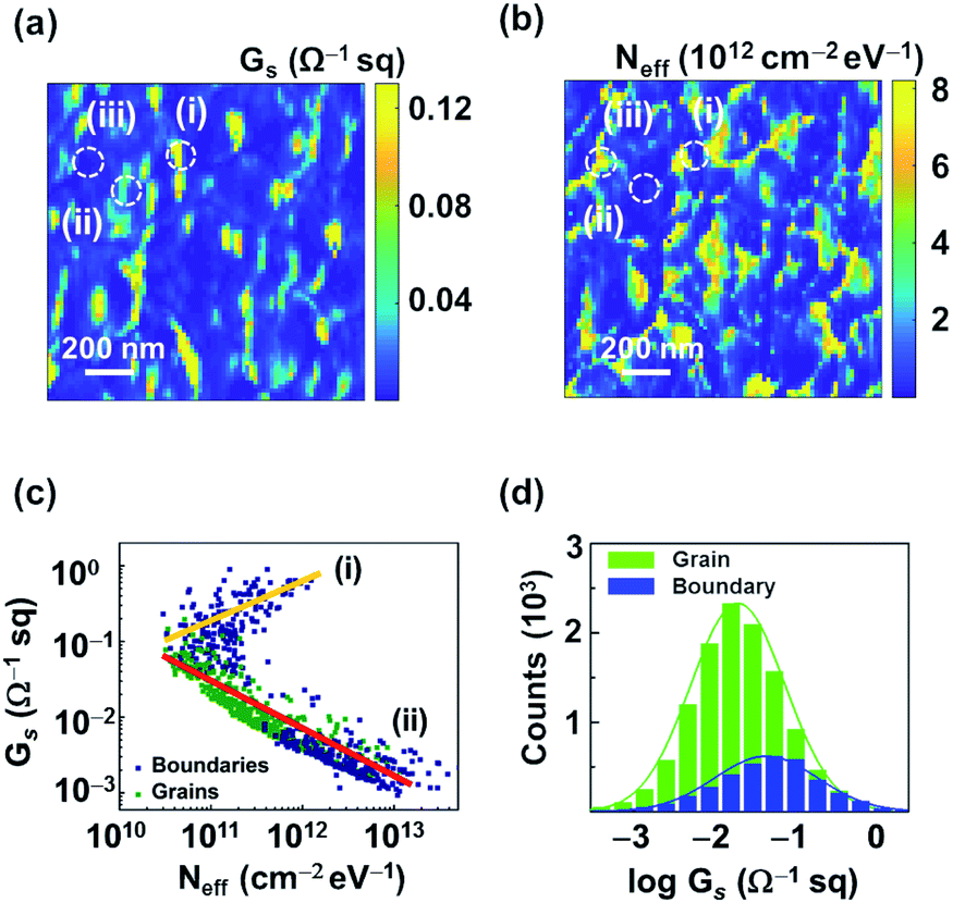 | ||
| Fig. 4 Nanoscale sheet-conductance and charge trap density mapping of an oxygen plasma-treated ITO thin film. (a) Sheet conductance (Gs) of the oxygen plasma-treated ITO thin film. The marks of (i) and (iii) represent the regions in a grain boundary, and (ii) corresponds to the regions inside a grain. (b) Charge trap density (Neff) of the ITO film. (c) Scattered plot showing the Gs and Neff after the oxygen plasma treatment. The slopes of the yellow and red fitting lines are 0.5 and −0.5, respectively. (d) Histograms showing the statistical distribution of sheet conductance values in grains and boundaries of the Gs maps in (a). | ||
Fig. 4b shows the effective charge trap density (Neff) map of the oxygen plasma-treated ITO thin film. The Neff value of grains (marked by (ii)) was ∼1.2 × 1011 cm−2 eV−1, while boundary regions had a value of ∼7.6 × 1011 cm−2 eV−1 (marked by (iii)). On average, the density of charge traps decreased by ∼70% after an oxygen plasma treatment. Presumably, oxygen ions and radicals could remove defects such as oxygen and cation interstitials, resulting in reduced amounts of charge traps.44 Also, note that boundary regions had large variations of charge trap density values like ∼8.9 × 1010 cm−2 eV−1 (marked by (i)) and ∼7.6 × 1011 cm−2 eV−1 (marked by (iii)), indicating that the number of charge traps decreased significantly in some grain boundary regions. Since the boundary regions had a rather large number of defects with different properties, we can expect that oxygen plasma treatment caused a more significant effect on the boundary regions than in the grain regions.41
A scatter plot between the sheet conductance (Gs) and the effective charge trap density (Neff) of the oxygen plasma-treated ITO thin film was plotted to further explore the effect of an oxygen plasma treatment (Fig. 4c). The data from grains and grain boundaries in maps are represented with green- and blue-colored squares, respectively. Each data point was extracted from the same location in the maps of sheet conductance Gs (Fig. 4a) and the corresponding charge trap density Neff (Fig. 4b). The results from the grain regions exhibited a rather large sheet conductance and small charge trap density values compared with that of untreated ITO films, as shown in Fig. 3d. However, they showed a similar scaling behavior to Gs ∝ N−0.5eff, indicating the diffusive transport in the grain regions even after the oxygen plasma treatment. On the other hand, the data points for boundary regions can be divided into two parts: (i) the regions with rather high sheet conductance values over ∼10−1 Ω−1 sq and (ii) those with rather low sheet conductance values below ∼10−1 Ω−1 sq. In the low sheet conductance regime (ii), the data exhibited a negative correlation as indicated by a red fitting line with a slope of ∼−0.5. The result indicates diffusive transport just like in grain regions of the ITO films. However, a positive correlation between the Gs and Neff was observed in the high conductance regions (i) of grain boundaries, as indicated by a yellow fitting line with a slope of ∼0.5. The positive correlation between the Gs and the Neff for boundary regions (i) could be attributed to the hopping conduction of charge carriers by localized states.20 In an ITO film, Sn atoms provide extra electrons as dopants.2,5 However, it has been reported that many of the Sn atoms in the boundary regions are often segregated and cannot work as dopants due to the low crystallinity in the boundary regions.40 In our studies, as the crystallinity of the boundary regions was improved after oxygen plasma treatment, Sn atoms in the boundary regions began to act as dopants, which should have generated localized dopant states inside an ITO band gap. Such localized states in the band gap can work as hopping sites, contributing to the hopping conductivity in the grain boundary regions. Previous studies showed that, when charge carriers flowed through hopping states, the relation between the Gs and the Neff can be written as follows20
| Gs ∝ N0.5eff | (3) |
It is consistent with our result as marked by the yellow fitting line (Fig. 4d), supporting the hopping transport in some grain boundaries of the oxygen plasma-treated ITO thin films. In our previous studies on other materials such as RGO and MoS2, the boundary regions exhibited diffusive transport, presumably due to rather large defect densities.20,24,25 The hopping conductivity in the boundary regions of the ITO is a somewhat anomalous behavior, presumably originating from a unique combination of elements in the ITO. These results show that our method can be utilized to explore the versatile effects of the oxygen plasma treatment on nanoscale charge transport in the grain structures of ITO thin films.
Fig. 4d shows the histogram of sheet conductance (Gs) values in grains and boundaries of the ITO thin film after an oxygen plasma treatment. The Gs values after the treatment were extracted from the sheet conductance map in Fig. 4a. Note that, after the oxygen plasma treatment, the sheet conductance of some of the boundaries was found to be larger than that of the grains, while the grain regions had much larger sheet conductance than the boundaries before the treatment (Fig. 3h). Also, it is interesting that the boundaries exhibited significantly increased sheet conductance upon treatment, while the sheet conductance increase of the grains was rather small. These results support the idea that the improved conductance of ITO films by the oxygen plasma treatment mainly originates from the improved conductance of the boundary regions, as we observed in the conductance map (Fig. 4a). Also, it is worth mentioning that the histogram plot of Neff shows significantly decreased noise sources in the boundaries after the oxygen plasma treatment (Fig. S3b, ESI†). Presumably, the oxygen plasma treatment improved the crystallinity more significantly in the boundary regions, resulting in reduced defects which are dominant noise sources.30 Our analyses allowed us to gain insights into the effects of oxygen plasma treatment on ITO films, which shows the versatility of our strategy.
4. Conclusions
We mapped the nanoscale effects of charge trap activities on charge transport in the grain structures of an oxygen plasma-treated ITO thin film. The results show that grain boundary regions exhibited a lower sheet conductance and a higher charge trap density than those inside the grains of the ITO thin film. We also observed that the sheet conductance and the charge trap density had the scaling relation of Gs ∝ Neff−0.5, indicating diffusive charge transport in the ITO thin film. In the oxygen plasma-treated ITO thin film, the sheet conductance increased by two times and the density of charge traps decreased by ∼70%, compared to those of the untreated ITO thin film. Interestingly, we observed the scaling behaviour of Gs ∝ Neff0.5 in some grain boundary regions of the oxygen plasma-treated ITO thin film, indicating the hopping transport. The result was attributed to the enhanced crystallinity and increased localized hopping states in the boundary regions after plasma treatment. Since our method allows one to map the nanoscale effect of charge traps on charge transport, it can be a powerful tool for basic research on the transport phenomena in ITO films and provide valuable guidelines for the development of advanced electronic devices.Author contributions
The key idea was conceived by Hyesong Jeon and Seunghun Hong. Hyesong Jeon performed most of the key experiments and data analyses. Jeongsu Kim, Shashank Shekhar, Jeehye Park, and Seunghun Hong helped perform some of the experiments and data analyses. The manuscript was written with the contribution of all authors.Conflicts of interest
There are no conflicts of interest to declare.Acknowledgements
This work was supported by the National Research Foundation of Korea (NRF) funded by the Ministry of Science and ICT (MSIT) of Korea (No. 2013M3A6B2078961 and 2020R1A2B5B02002152). S. H. would like to acknowledge the support from the Ministry of Trade, Industry & Energy (MOTIE, Korea) (No. 20012390), Samsung Electronics Co. Ltd. (No. 201209-07908-01) and the European Research Council (ERC) under the European Union's Horizon 2020 programme (grant agreement no. 682286).References
- S. Ray, R. Banerjee, N. Basu, A. K. Batabyal and A. K. Barua, J. Appl. Phys., 1983, 54, 3497 CrossRef CAS.
- R. B. H. Tahar, T. Ban, Y. Ohya and Y. Takahashi, J. Appl. Phys., 1998, 83, 2631–2645 CrossRef.
- H. Kim, C. M. Gilmore, A. Piqué, J. S. Horwitz, H. Mattoussi, H. Murata, Z. H. Kafafi and D. B. Chrisey, J. Appl. Phys., 1999, 86, 6451 CrossRef CAS.
- M. Shakiba, A. Kosarian and E. Farshidi, J. Mater. Sci.: Mater. Electron., 2017, 28, 787–797 CrossRef CAS.
- T. Omata, H. Fujiwara, S. Otsuka-Yao-Matsuo and N. Ono, Appl. Phys. A: Mater. Sci. Process., 2000, 71, 609–614 CrossRef CAS.
- N. R. Armstrong, P. A. Veneman, E. Ratcliff, D. Placencia and M. Brumbach, Acc. Chem. Res., 2009, 42, 1748–1757 CrossRef CAS PubMed.
- N. G. Patel, P. D. Patel and V. S. Vaishnav, Sens. Actuators, B, 2003, 96, 180–189 CrossRef CAS.
- T. Kuwabara, T. Nakayama, K. Uozumi, T. Yamaguchi and K. Takahashi, Sol. Energy Mater. Sol. Cells, 2008, 92, 1476–1482 CrossRef CAS.
- M. H. Ahn, E. S. Cho and S. J. Kwon, Appl. Surf. Sci., 2011, 258, 1242–1248 CrossRef CAS.
- Y. H. Liau, N. F. Scherer and K. Rhodes, J. Phys. Chem. B, 2001, 105, 3282–3288 CrossRef CAS.
- L. Bhrdos and M. Libra, Vacuum, 1989, 39, 33–36 CrossRef.
- H. Kim, J. S. Horwitz, G. Kushto, A. Pique, Z. H. Kafafi, C. M. Gilmore and D. B. Chrisey, J. Appl. Phys., 2000, 88, 6021 CrossRef CAS.
- Z. Ghorannevis, E. Akbarnejad and M. Ghoranneviss, J. Theor. Appl. Phys., 2015, 9, 285–290 CrossRef.
- M. Nisha, S. Anusha, A. Antony, R. Manoj and M. K. Jayaraj, Appl. Surf. Sci., 2005, 252, 1430–1435 CrossRef CAS.
- F. E. Akkad, M. Marafi, A. Punnoose and G. Prabu, Phys. Status Solidi, 2000, 177, 445 CrossRef.
- C. V. R. Vasant Kumar and A. Mansingh, J. Appl. Phys., 1989, 65, 1270–1280 CrossRef.
- N. M. Ahmed, F. A. Sabah, H. I. Abdulgafour, A. Alsadig, A. Sulieman and M. Alkhoaryef, Results Phys., 2019, 13, 102159 CrossRef.
- J. Xu, Z. Yang, X. Zhang, H. Wang and H. Xu, J. Mater. Sci.: Mater. Electron., 2014, 25, 710–716 CrossRef CAS.
- C. C. Wu, C. I. Wu, J. C. Sturm and A. Kahn, Appl. Phys. Lett., 1997, 70, 1348–1350 CrossRef CAS.
- M. Yang, T. Y. Kim, T. Lee and S. Hong, Sci. Rep., 2018, 8, 15822 CrossRef PubMed.
- N. Shin, J. Kim, S. Shekhar, M. Yang and S. Hong, Carbon, 2019, 141, 59–66 CrossRef CAS.
- S. Shekhar, D. Cho, H. Lee, D. G. Cho and S. Hong, Nanoscale, 2016, 8, 835–842 RSC.
- H. K. Kim, H. Y. Ha, J. H. Bae, M. K. Cho, J. Kim, J. Han, J. Y. Suh, G. H. Kim, T. H. Lee, J. H. Jang and D. Chun, Sci. Rep., 2020, 10, 13699 CrossRef CAS PubMed.
- H. Lee, D. Cho, S. Shekhar, J. Kim, J. Park, B. H. Hong and S. Hong, ACS Nano, 2016, 10, 10135–10142 CrossRef CAS PubMed.
- S. Shekhar, H. Lee, D. Cho, M. Yang, M. Lee and S. Hong, Carbon, 2019, 148, 326–335 CrossRef CAS.
- D. Cho, T. Hwang, D.-g. Cho, B. Park and S. Hong, Nano Energy, 2018, 43, 29–36 CrossRef CAS.
- R. N. Chauhan, R. S. Anand and J. Kumar, Thin Solid Films, 2014, 556, 253–259 CrossRef CAS.
- S. Talu, S. Stach, D. Raoufi and F. Hosseinpanahi, Electron. Mater. Lett., 2015, 11, 749–757 CrossRef CAS.
- M. Hilal and J. I. Han, Synth. Met., 2018, 245, 276–285 CrossRef CAS.
- S. S. Yeh, W. M. Hsu, J. K. Lee, Y. J. Lee and J. J. Lin, Appl. Phys. Lett., 2013, 103, 123118 CrossRef.
- H.-C. Lee and O. O. Park, Vacuum, 2004, 75, 275–282 CrossRef CAS.
- H. Nanto, T. Minami, S. Orito and S. Takata, J. Appl. Phys., 1988, 63, 2711 CrossRef CAS.
- D. Mergel and Z. Qiao, J. Phys. D: Appl. Phys., 2002, 35, 794–801 CrossRef CAS.
- S. Dasgupta, M. Lukas, K. Dossel, R. Kruk and H. Hahn, Phys. Rev. B: Condens. Matter Mater. Phys., 2009, 80, 085425 CrossRef.
- G. Reiss, J. Vancea and H. Hoffmann, Phys. Rev. Lett., 1986, 56, 2100–2103 CrossRef PubMed.
- M. Balestrieri, D. Pysch, J. P. Becker, M. Hermle, W. Warta and S. W. Glunz, Sol. Energy Mater. Sol. Cells, 2011, 95, 2390–2399 CrossRef CAS.
- M. Si, J. Andler, X. Lyu, C. Niu, S. Datta, R. Agrawal and P. D. Ye, ACS Nano, 2020, 14, 11542–11547 CrossRef CAS PubMed.
- J. Stotter, Y. Show, S. Wang and G. Swain, Chem. Mater., 2005, 17, 4880–4888 CrossRef CAS.
- R. S. Datta, N. Syed, A. Zavabeti, A. Jannat, M. Mohiuddin, M. Rokunuzzaman, B. Yue Zhang, M. A. Rahman, P. Atkin, K. A. Messalea, M. B. Ghasemian, E. Della Gaspera, S. Bhattacharyya, M. S. Fuhrer, S. P. Russo, C. F. McConville, D. Esrafilzadeh, K. Kalantar-Zadeh and T. Daeneke, Nat. Electron., 2020, 3, 51–58 CrossRef CAS.
- I. A. Rauf and J. Yuan, Mater. Lett., 1995, 25, 217–222 CrossRef CAS.
- J. H. Lee, Y. H. Kim, S. J. Ahn, T. H. Ha and H. S. Kim, Mater. Sci. Eng. B, 2015, 199, 37–41 CrossRef CAS.
- J. Kim, D. Hong, H. Lee, Y. Shin, S. Park, Y. Khang, M. Lee and S. Hong, J. Phys. Chem. C, 2013, 117, 19721–19728 CAS.
- Q. Hou, J. Buckeridge, T. Lazauskas, D. Mora-Fonz, A. A. Sokol, S. M. Woodley and C. R. A. Catlow, J. Mater. Chem. C, 2018, 6, 12386–12395 RSC.
- I. Irfan, S. Graber, F. So and Y. Gao, Org. Electron., 2012, 13, 2028–2034 CrossRef CAS.
- M. Liu and H. K. Kim, Appl. Phys. Lett., 2004, 84, 173–175 CrossRef CAS.
- S. I. Jun, T. E. McKnight, M. L. Simpson and P. D. Rack, Thin Solid Films, 2005, 476, 59–64 CrossRef CAS.
Footnote |
| † Electronic supplementary information (ESI) available: Calculation of sheet-resistance by a finite element method; calculation of charge trap density by a resistance network model; statistical distribution of charge trap density; macroscopic current–voltage curves for untreated and plasma treated ITO; XRD, XPS and EDX spectra of untreated and plasma treated ITO. See DOI: 10.1039/d1na00175b |
| This journal is © The Royal Society of Chemistry 2021 |