
 Open Access Article
 This Open Access Article is licensed under a Creative Commons Attribution-Non Commercial 3.0 Unported Licence
Modified vapor phase deposition technology for high-performance uncooled MIR PbSe detectors†
Jijun Qiu *,
Yun Liu,
Guodong Zhang,
Kanghao Shi,
Yanzhen Li and
Yingmin Luo
*,
Yun Liu,
Guodong Zhang,
Kanghao Shi,
Yanzhen Li and
Yingmin Luo
School of Microelectronics, Dalian University of Technology, Dalian, 116024, PR China. E-mail: jjqiu@dlut.edu.cn
First published on 28th October 2021
Abstract
The low performance of middle infrared (MIR) PbSe detectors fabricated from vapor phase deposition (VPD) technology restricts the rapid development of VPD technology and detector commercialization. A modified VPD process was proposed to duplicate the microstructural features of high-performance CBD-PbSe detectors for a breakthrough in the VPD technology. A peak detectivity D* of 1.6 × 1010 cm Hz1/2 W−1 at 298 K was achieved under the optimized sensitization, approaching the best performance of CBD-PbSe detectors. Through the contrasting various microstructures obtained from diverse methods, the nanoparticle self-assembly structure in VPD-PbSe oriented rod-like crystals is an important factor for the IR sensitivity. The microstructural evolution demonstrated that there is a large space to grow for VPD-PbSe detectivity D* via eliminating the voids formed in the iodine-sensitization process. The increased performance indicates that the modified VPD technology can provide technical support for the manufacturing of the megapixel uncooled lead-salt FPA imager and accelerate its industrialization.
I Introduction
Uncooled lead-salt focal plane array (FPAs) detectors are making a comeback for niche military applications after having almost disappeared from view since the 1980s.1–8 Compared with IR thermal detectors such as microbolometers, polycrystalline lead-salt infrared detectors present many remarkable characteristics, such as fast response speed, high frame rate, and good sensitivity in the MIR (1–5 μm) spectral band at room temperature, which are pressing needs for the intelligence industry and defence. However, lead-salt detectors have been stigmatized for a long time due to limitations in material processing6–28 and poorly understood physics.12,28–37 The research & development of lead-salt detectors was opened again after an uncooled lead-salt 320 × 240 FPA imager shown in Fig. 1 was presented by Imager Litton Electro-Optical Systems in 2001.4,5 After this important milestone, research has been carried out in this direction with the objective of improving device performances and reaching technological industrial maturity.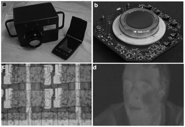 | ||
| Fig. 1 CBD-PbSe FPA camera. (a) Northrop's prototype lead salt camera, (b) PbSe FPA mounted in 2105 package, (c) micrograph of PbSe FPA (1000×) and (d) imagery using lead-salt camera.5 | ||
By now, two available technologies were employed to fabricate uncooled lead-salt FPA imagers: a standard chemical bath deposition (CBD) and vapor phase deposition (VPD). Although CBD technology was utilized since WWII and developed to be a standard technology for lead-salt IR detectors, it exhibits a number of drawbacks, such as large 1/f noise, poor stability, bad IR response uniformity and high dielectric constant. These flaws are precluding seriously the development of CBD technology and communalization of uncooled lead-salts FPA imagers.4–19 During last 20 years, an innovative technology named VPD technology was developed by Spanish MoD laboratories (CIDA) and New Infrared Technologies, S.L. (NIT).20–28 Technological evolution of VPD PbSe technology is shown in Fig. 2. Being a simple and affordable technology, the most remarkable characteristics and advantages of VPD technology are: good uniformity in large areas, good reproducibility, long term stability, suitable for 2D FPAs and good compatibility with existing Si CMOS technology. Therefore, since the appearance of VPD technology, it has been inspiring high hopes in the filling the existing gap in high-resolution uncooled MWIR uncooled FPA camera. However, there is a fatal flaw of lower IR detectivity, which is a major obstacle to the rapid development of VPD technology. The detectivity of VPD-PbSe detectors (D*) has been in the range of 2–5 × 109 cm Hz1/2 W−1 since 2000, which is one order of magnitude lower than that of CBD-PbSe detectors.20–28,32 The lower performance has been limiting VPD-PbSe detector's wild applications in aerospace, national defense, industry and other frontier. To our knowledge, a 128 × 128 2D FPA camera with frame rate above 2000 Hz is commercially available, representing the highest level of VPD-PbSe FPA imagers.26,28
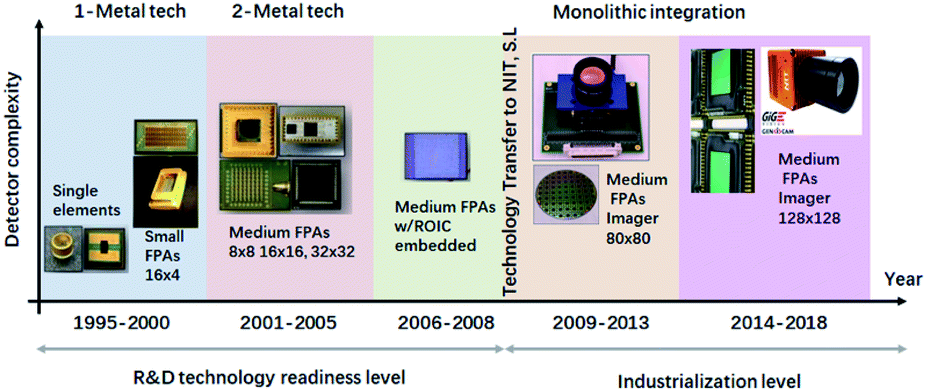 | ||
| Fig. 2 Technological evolution of VPD-PbSe technology. | ||
Based on our pervious numerous of studies on high-performance CBD-PbSe detectors,8,9,17,18,41 a conclusion is indisputable that the microstructural feature of as-grown CBD-PbSe films is critical in high performance of PbSe detectors. According to this clue, herein the VPD process was modified to duplicate exactly the microstructure of CBD-PbSe film by decreasing the vacuum degree and deposition temperatures. Assisted with an optimized sensitization,8 a specific high-temperature thermal treatment to convert as-grown film into an active materials sensitive to the IR radiation, a peak detectivity D* of 1.6 × 1010 cm Hz1/2 W−1 for PbSe MIR detector was achieved at room-temperature, which approaches the best performance of standard CBD-PbSe detectors. There is no doubt that the modified VPD technology shows a great potential in industry and military applications which are demanding rugged, low-cost, high-speed and high performance uncooled NIR and MIR FAP imagers, such as automatic and auxiliary driving of automobiles, industrial quality inspection, manufacturing process control, imaging infra-red (IIR) seeker system etc.
II Experiment
Device fabrication and characterization
PbSe films were fabricated on cleaned glass slides by using VPD and CBD technologies. For CBD technology, the aqueous precursor was prepared via dissolving sodium hydroxide, lead acetate, and selenosulfate with a concentration ratio of 12![[thin space (1/6-em)]](https://www.rsc.org/images/entities/char_2009.gif) :1:1.18 The cleaned glass substrates were transferred into the aqueous precursor and maintained at 80 °C for 3.0 h and at 3 °C for 240 h. Hydrothermal growth was carried out in a hydrothermal reaction vessel at 180 °C for 1.0 h. For traditional VPD technology, 99.999% PbSe was deposited on cleaned glass substrates by thermal evaporation in 10−4 Pa for 1.0 h at 300 °C substrate temperature. For modified VPD method, the vacuum degree was decreased to 10−2 Pa by introducing the oxygen gas for duplicating the microstructural features of high-performance CBD-PbSe films. Furthermore, the deposition was carried out at 130 °C and room-temperature for 3 h with a growth rate of 60–70 nm min−1.
:1:1.18 The cleaned glass substrates were transferred into the aqueous precursor and maintained at 80 °C for 3.0 h and at 3 °C for 240 h. Hydrothermal growth was carried out in a hydrothermal reaction vessel at 180 °C for 1.0 h. For traditional VPD technology, 99.999% PbSe was deposited on cleaned glass substrates by thermal evaporation in 10−4 Pa for 1.0 h at 300 °C substrate temperature. For modified VPD method, the vacuum degree was decreased to 10−2 Pa by introducing the oxygen gas for duplicating the microstructural features of high-performance CBD-PbSe films. Furthermore, the deposition was carried out at 130 °C and room-temperature for 3 h with a growth rate of 60–70 nm min−1.
Measurement methods
Subsequently, as-grown PbSe films were sensitized in O2 atmospheres at 420 °C for 1 h, followed by O2 and I2 atmosphere at 380 °C for 10–30 min. To fabricate the PbSe detectors, 100 nm thick gold thin films were deposited by thermal evaporation over two sides of the 4 × 2 mm2 post iodine sensitized PbSe film with a 0.07 mm2 active area. The detectivity was measured using a SR830 DSP lock-in amplifier and collimated black body at 500 K at room temperature (298 K) with under 750 Hz chopping frequency modulation. The devices were biased at 50 V mm−1 using Agilent E3612A source, with a load resistor matched to the detector resistance. The distance between the blackbody and the detectors was 20 cm.III Results and discussion
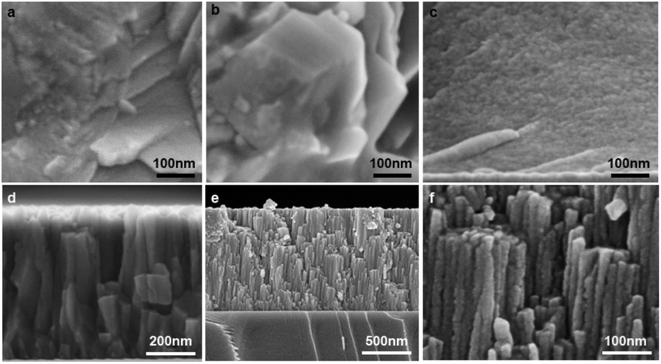
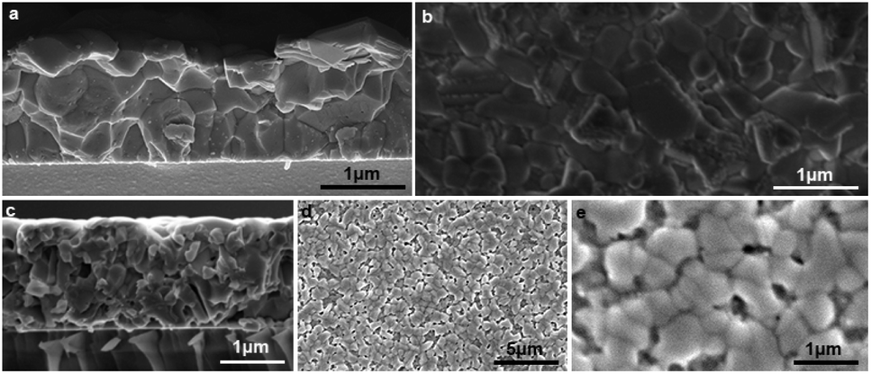
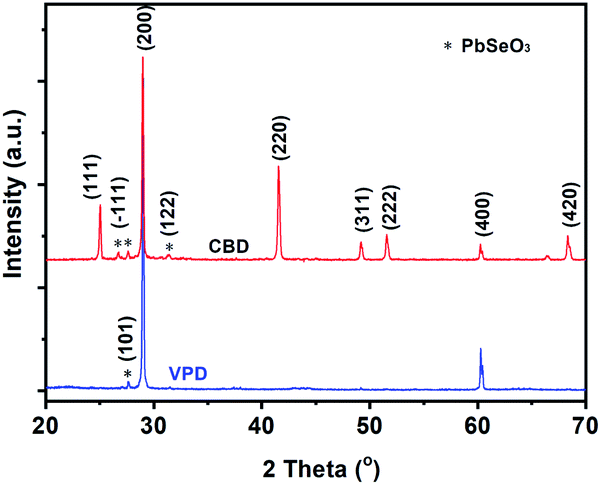
The micro-morphologies of PbSe films fabricated from CBD, traditional VPD and modified VPD technologies were shown in Fig. 3. The side-view of CBD-PbSe films in Fig. 3(a) displayed a rough and compact layer constituted by the oriented pyramidal-shape micro-polycrystalline, which was confirmed by the top-view FESEM image in Fig. 1(c). Based on the appearance of a strong peak at 29.14° in its XRD pattern showing in Fig. 4, corresponding to PbSe (200) facet, it sees that the pyramidal-shape micro-polycrystalline were mostly oriented along [111] direction. Higher resolution side-view FESEM in Fig. 3(b) revealed that every micron-size pyramidal crystallite was self-assembly of very small nanocrystals. The size of nanocrystals is of 8–12 nm. This structural feature was attributed to the synergistic effect of initial ion-by-ion (IBI) growth model and later Oriented-Attachment (OA) growth model, considering lower surface energy of (100) facets.39 Through the contrast various microstructures obtained from diverse methods, we figured that the self-assembly structure occurring in as-grown films was a most important factor for PbSe IR-response. No any infrared response was observed from the PbSe films composed of micro-size pyramidal crystal without self-assembly nanoparticles by using hydrothermal method at 180 °C (Fig. 5(b)) or the films packed by disordered nanoparticles synthesized at 3 °C CBD growth temperature (Fig. 5(c)), regardless of the sensitized conditions.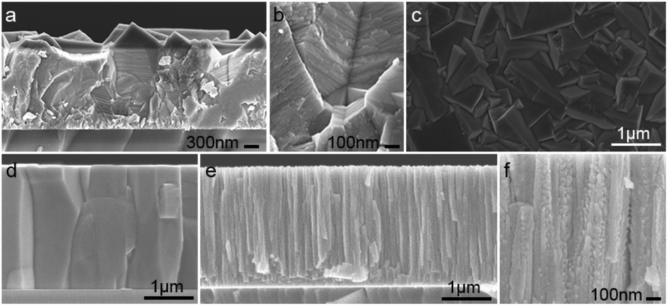 | ||
| Fig. 3 Typical microstructural features of as-grown PbSe films. (a) Low-magnification and (b) high-magnification side-view and (c) top-view FESEM image of CBD-PbSe films grown 80 °C for 3.0 h. (d) Low-magnification side-view FESEM image of traditional VPD-PbSe film fabricate at 300 °C in 2 × 10⁻⁴ Pa. (e) Low- and (f) high-resolution side-view FESEM image of modified VPD-PbSe film fabricated at 25 °C substrate temperature in 2 × 10⁻² Pa. | ||
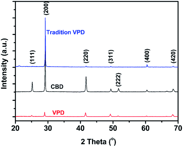 | ||
| Fig. 4 XRD patterns of PbSe films fabricated from traditional VPD, CBD and modified VPD technologies. | ||
 | ||
| Fig. 5 Typical microstructural features of as-grown PbSe films fabricated from various methods at different growth temperatures and O2 pressure. (a) CBD at 80 °C, (b) hydrothermal at 180 °C, (c) CBD at 3 °C, (d) VPD at 130 °C in 5 × 10⁻³ Pa O2 pressure; (e and f) VPD at 130 °C in 4 × 10⁻² Pa O2 pressure. | ||
The recent studies9,18,33–37,41 have shown that iodine is key element to trigger the IR-response of PbSe by forming PbI2, PbSeIx or Pb–Se–O–I phase at the surface and interfaces between PbSe grains. Due to hard diffusion of iodine in the large PbSe single-crystal grains, it is difficult to form a continuous PbI2, PbSeIx or Pb–Se–O–I phases transporting channels for photo-generated electrons in the whole PbSe film during sensation process. At the same time, large single-crystal grain was disadvantageous for oxygen passivation to eliminate the defects in the PbSe crystalline. There were lots of defects in an amorphous nanoparticle PbSe film synthesized at 3 °C.38 These defects can't be completely eliminated by the sensitization process. The surviving defects become the recombination centres for photo-generated electrons and holes, then decreased the carrier lifetime, resulting in unsensitive for IR radiation.
No infrared responsivity was detected in sensitized traditional-VPD method, confirming that the key role of self-assembly microstructure of CBD as-grown PbSe films on the infrared response. A typical compact columnar structure of traditional VPD-PbSe films was shown in Fig. 3(c), and one sharp and narrow XRD peak corresponding to PbSe (200) facet in Fig. 4 indicates that columnar crystals with 1 μm size grow preferentially along [200] orientation. By introducing O2 into the VPD deposition chamber and depositing at 25 °C substrate temperature, a microstructure similar with CBD-PbSe film was achieved, as shown in Fig. 3(e) and (f). It was a smooth and compact film constituted by (200) oriented PbSe nanorod-like clusters with a uniform distribution of 120 nm. High-resolution side-view FESEM in Fig. 3(f) obviously displayed that the nanorods were built by self-assembly of nanoparticles, which is originated from OA growth mechanism.
The influence of vacuum degree and substrate temperature on the microstructures of VPD-PbSe films were studied, shown in Fig. 5(d) and (e) show the typical microstructural features of VPD-PbSe films by various O2 pressure at 130 °C growth temperature. With the increase of the O2 pressure from 10−4 to 5 × 10⁻³ Pa, the size of columnar crystals decreased from 1 μm to 50 nm, presenting a single crystal rode-like crystals as shown in Fig. 5(d). With further increasing the O2 pressure to 4 × 10⁻² Pa, one-dimensionally ordered self-assembly of nanocrystals could be obviously observed from Fig. 5(e) and (f). Therefore, there seemed to be no doubt that high O2 pressure and low growth temperature contribute to the formation of microstructure of nanorods composed of self-assembled nanocrystals. It is well known that low growth temperature inhibits the spontaneous growth of columnar PbSe grain originated from dynamic driving. At the same time, the absorbed oxygen on the surfaces of PbSe nanoparticles lead to a transformation of growth mechanism from IBI to OA model.40 Subsequent, detectivity texting results proved that the optimized substrate temperature is at the range of 25–130 °C under O2 pressure of 10−2 Pa. More typical morphologies of VPD-PbSe as-grown films could be obtained from ESI.†
Beside of microstructure, the modified VPD technology also duplicates the phase composition of PbSe film fabricated from CBD technology, identified by XRD patterns showing in Fig. 4. Although a slight difference in intensities, the all PbSe facets in CBD-film XRD pattern appeared in the pattern of modified VPD film.
It is well known that once deposited, lead-salt film is alive to IR radiation after suffering thermal-sensitization process in O2 and/or I2 atmosphere.18,32 By now, the sensitization processes vary with the individual group. In our case, an optimized two-step sensitization process was employed, including oxidization at 420 °C for 1 h, followed by iodization at 380 °C for 10 min.
The responsivity R and specific detectivity D* were obtained as described in our previous work by using the definition as shown below:
where Is and In are the measured detector output signal and noise currents, A is the device detection area, Δf is the noise bandwidth, and Pi is the incident radiant power. Peak responsivity Rpeak and peak detectivity D* are then calculated through a conversion factor defined in ref. 17.
Finally, a room-temperature peak detectivity D* of 1.6 × 1010 cm Hz1/2 W−1 was achieved at blackbody 500 K under 750 Hz chopping frequency modulation, which outperforms the VPD-PbSe detectors reported by NIT, and approaches the D* of 2.8 × 1010 cm Hz1/2 W−1 of the CBD-PbSe detector.17
Fig. 6 presented the microstructures of CBD-and VPD-PbSe detectors. The side- and top-view of FESEM image of CBD detector showing in Fig. 6(a) and (b) demonstrated the sensitized CBD-PbSe grains was 0.5–1 μm, and have blunted edges and a surface roughness of 0.2–0.3 μm. We deem that the morphological evolution before and after sensitization was attributed to in sequence (1) the oxygen passivation of intrinsic  and
and  defects within PbSe nano-crystals; (2) the recrystallization of PbSe nano-crystals and (3) the formation of PbSeO3 or Pb–Se–O–I phase around the PbSe crystals.9,18 The smaller the nanocrystal is, more easily the oxygen diffuses and more complete the passivation, the better the nanocrystal quality. Subsequently, the nanocrystals with high crystal quality recrystallize to form large microcrystals powered by the thermodynamic driving force (420 °C). The two above-mentioned reasons could be vitrified by the enhanced peak intensities and the narrowed full width at half maximum (FWHM) related to PbSe facets in the XRD patterns, showing in Fig. 7.
 | ||
| Fig. 6 Typical microstructural features of sensitized PbSe films. (a) Side-view and (b) top-view FESEM image of sensitized CBD-PbSe films. (c) Low-magnification side-view and (d) low-magnification and (e) high-magnification top-view FESEM image of sensitized modified VPD-PbSe film. | ||
 | ||
| Fig. 7 XRD Patterns of sensitized PbSe detectors fabricated from CBD and modified VPD technologies. | ||
An exactly the same evolvements in morphology and phase composition were observed in the sensation process of VPD-PbSe film, as shown in Fig. 6(c)–(e) and 7. The morphology of sensitized VPD-PbSe showed a small PbSe grains of 150–200 nm and a smooth surface roughness of less than 100 nm. The substantial improvement in the distribution of PbSe microcrystal size and the surface roughness can help to improve the performance uniformity and yield of lead-salt IR-sensitive films, which is key for FPA imaging system. In comparation with compact tissue of CBD-PbSe sensitized film, there were many voids in the sensitized VPD-PbSe films, which was considered as the reason for the D* of VPD-PbSe detector lower than that of CBD-PbSe detector in our case. Therefore, detectivity D* of VPD-PbSe detectors has great developing opportunity by further optimizing the sensitization process to eliminate the voids in VPD-PbSe detectors.
Note, there were only (200) and (400) peaks surviving in the sensitized VPD-PbSe XRD pattern in Fig. 7. This is caused by a mixed Oriented Attachment and Ostwald Ripening (OR) growth pathway during the recrystallization process.38 First, adjacent small PbSe particles with common crystallographic orientations combine to form large one by OA mechanism in initial annealing stage. Then larger PbSe grains with high orientation are formed by an interface-reaction-limited mass transfer from smaller particles. The PbSe (100) facet is significantly lower in energy than the (111) facet, PbSe shows a tendency to form clusters with a rectangular symmetry with (100) orientation on the glass at low temperature, or rods with a cubic symmetry at high temperature, as shown in Fig. 3(e) and (d), respectively. After high-temperature recrystallization, the PbSe particles with (100) orientation merges into big grains by OA growth mechanism, companying with significant increase of (100) intensity contributed from recrystallization and oxygen passivation. At the same time, other PbSe small particles with (220), (311) orientation slowly disappear for the interface-reaction-limited mass transfer, and merge into large PbSe grains with (100) orientation. Finally, there are only (200) and (400) facets with strong intensities observed in XRD patterns.
The influence of resistance on the detectivity was analysed, and was summarized in Table 1. Based on the p–n charge separation model for the enhanced photoconduction detection mechanism,33 the resistance of PbSe detector was regulated by the thickness of PbSeO3,16 PbSeIx (ref. 35) or PbI2 (ref. 34–37) wrapping in PbSe microcrystals, which was dominated by the iodine-sensitization time. With increasing the iodine-sensitization time to 30 min, the resistance of detector significantly increases by almost four orders of magnitude up to 8 MΩ. The best detectivity D* was achieved at resistance of 0.2 MΩ with a 0.2 μV noise and a 9150 signal/noise (S/N). It is found that the signal and noise reach the maximum as the resistance kept on increasing to 0.4 MΩ. However, the increased multiple in noise (3) was more than the multiple in signal (1.4), resulting in an order of magnitude reduction in the detectivity D* (2.0 × 109 cm Hz1/2 W−1). Subsequently, the signal and noise drop synchronously with further increasing resistance to 8 MΩ. Based on the morphological evolution, there was a reasonable prospect that the size and number of voids mount with increase of the resistance (iodine-sensitization time), resulting in increasing of the noise. The maximum signal of 2490 μV at 0.4 MΩ for VPD-PbSe detector almost approached to the signal of best CBD-PbSe detector obtained at 4 MΩ, indicating that the future research of VPD-PbSe technology is focus on the noise reduction while maintaining the maximum signal.
| Time, min | Resistance, MΩ | Signal, V | Noise, μV | D* (λp, 750, 1), cm Hz1/2 W−1 |
|---|---|---|---|---|
| 0 | 0.002 | — | — | — |
| 5 | 0.07 | 534 | 0.6 | 1.7 × 10⁹ |
| 10 | 0.2 | 1830 | 0.2 | 1.6 × 10¹⁰ |
| 20 | 0.4 | 2490 | 1.9 | 2.0 × 10⁹ |
| 30 | 8.0 | 1083 | 0.5 | 4.0 × 10⁹ |
| 20(CBD) | 4.0 | 2643 | 0.2 | 2.8 × 10¹⁰ |
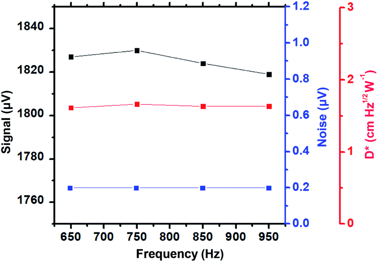
The typical frequency response of the optimized VPD-PbSe detector was shown in Fig. 8. It's always been known that the lead-salt detector has a 1/f noise characteristic, so the lower frequencies have higher noise and consequently a lower D* value. The detectivity D* relatively constant after the chopping frequency was increased to 950 Hz. For PbSe detectors, 1 kHz is chosen as a standard chopping frequency because it is away from the 1/f noise but lower than the time constant response limit.
 | ||
| Fig. 8 The dependence of chopping frequency on the performance of VPD-PbSe detectors. | ||
Base on the dependency of the detectivities on the microstructures of PbSe films obtained from various fabrication technologies, a qualitative explanation for the optimum microstructure is given. It is obvious that the performance of PbSe photoconductors is dominated by the crystal quality, orientation and size of PbSe particles, which depends on the fabrication technology and deposition temperature.44,45 The crystal quality determinates the life time of the photogenerated carriers. Higher crystal quality is, fewer defects inside crystal, lower number of recombination centres of photogenerated electrons and holes, longer the lifetime of photogenerated carriers, resulting in an enhanced detectivity. The ordered crystal orientation of PbSe particles contributes to the glide of the defects or dislocations inside crystals46 during the oxidization step, resulting in an improved carrier lifetime. Based on the p–n charge separation model, the particle size is critical to the formation of p–n heterojunction interface. Larger particle is, denser the structure, harder the iodine diffuses, fewer the p–n heterojunction interface, the more difficult for the photogenerated carriers, resulting in a lower infrared responsivity. Suffering from the process modifying, the microstructure of VPT PbSe film changes from typical microrods (Fig. 3(d)) into nanorods comprised of self-assembled nanoparticles (Fig. 3(f)), which helps to eliminate the defects and dislocation during the first-step sensitization, resulting in a longer carrier lifetime. At the same time, small size and loose structure make the iodine diffusion easier to form larger number of p–n heterojunction interface during the second-step sensitization, speeding the separation of photogenerated carriers.
IV Conclusion
In summary, we tried to replicate the microstructure of high-performance CBD-PbSe detectors by employing the modified VPD technology for breakthrough the VPD technical bottleneck of low detectivity. Microstructural characteristics of microcrystal comprising self-assembled nanoparticles and phase composition were exactly duplicated under 10−2 Pa O2 pressure and 25 °C growth temperature. Suffered from the optimized sensitization involving an oxidization at 420 °C for 1 h and an iodization at 380 °C for 10 min, a room-temperature peak detectivity D* of 1.6 × 1010 cm Hz1/2 W−1 was achieved at blackbody 500 K under 750 Hz chopping frequency modulation, which approaches the best performance of CBD-PbSe detectors, as shown in Fig. 9. The microstructural evolution demonstrated that there is still plenty of room to promote the detectivity of VPD-PbSe detectors via eliminating the voids formed in the sensitization process to reduce the noise. This indicates that the modified VPD technology can provide a technical solution for the manufacturing of the megapixel uncooled lead salt FPA imaging system, which has wide application in military, commercialization and civilian, such as Imaging Infra-Red (IIR) seeker system, automatic and automatic an auxiliary driving of automobiles, industrial quality inspection, manufacturing process control etc.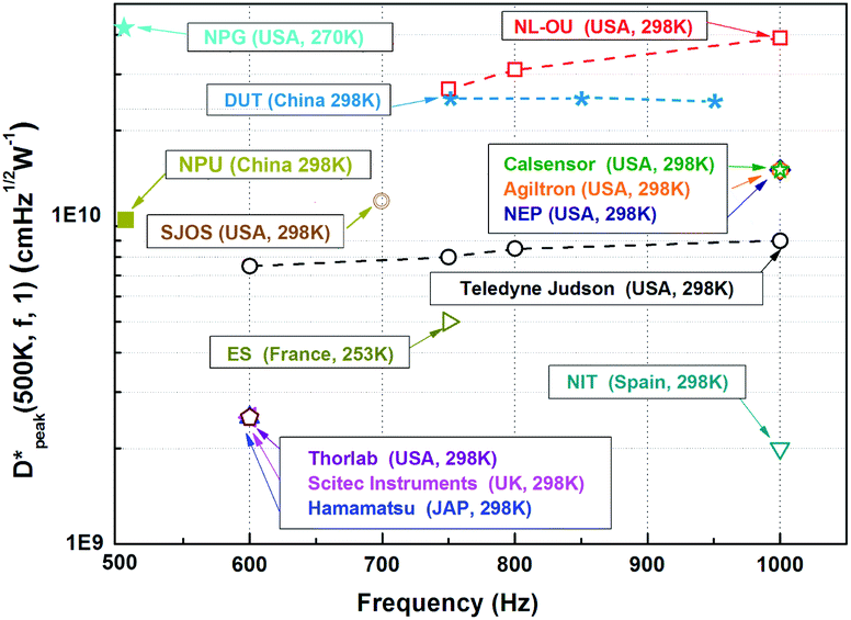 | ||
| Fig. 9 Comparison of D* value reported by various institutes.6,8,32,42–43 | ||
Conflicts of interest
There are no conflicts to declare.Acknowledgements
This research was funded by the Dalian Science and Technology Innovation Fund (2020JJ26GX022) and Fundamental Research Funds for the Central Universities (Grant No. DUT19RC(3)032).Notes and references
- https://www.wdzj.com/hjzs/ptsj/20190404/972424-1.html.
- https://www.militaryaerospace.com/unmanned/article/16713998/darpa-launches-wired-program-to-develop-affordable-waferscale-infrared-sensors.
- H. Yang, X. J. Li, G. D. Wang and J. B. Zheng, Lead Selenide Polycrystalline Coatings Sensitized Using Diffusion and Ion Beam Methods for Uncooled Mid-Infrared Photodetection, Coatings, 2018, 8, 444 CrossRef.
- T. Beystrum, N. Jacksen, M. Sutton, M. Preis and C. Walmsley, Low-cost 320x240 lead salt focal plane array, Presented in part at the Infrared Imaging Systems: Design, Analysis, Modeling, and Testing XII, 2001, vol. 4372, pp. 96–104 Search PubMed.
- T. Beystrum, R. Himoto, N. Jacksen and M. Sutton, Low-cost PbSalt FPAs, Presented in part at the, Infrared Technology and Applications XXX, 2004, vol. 5406, pp. 287–294 Search PubMed.
- D. Shelton, J. Sigley, R. Nicholas and R. Driggers, Potential and limitations for very-high-operating-temperature (VHOT) MWIR focal plane arrays using halogen-passivated PbSe, Presented in part at the, Infrared Technology and Applications XLIV, 2018, vol. 10624, p. 1062411 Search PubMed.
- G. Vergara, R. Linares Herrero, R. Gutíerrez Álvarez, C. Fernández-Montojo, L. J. Gómez, V. Villamayor, A. Baldasano Ramírez and M. Montojo, 80 × 80 VPD PbSe: the first uncooled MWIR FPA monolithically integrated with a Si-CMOS ROIC, Presented in part at the, Infrared Technology and Applications XXXIX, 2013, vol. 8704, p. 87041M Search PubMed.
- B. Weng, J. Qiu, L. Zhao, Z. Yuan, C. Chang and Z. Shi, Recent development on the uncooled mid-infrared PbSe detectors with high detectivity, Presented in part at the, Quantum Sensing and Nanophotonic Devices XI, 2014, vol. 8993, p. 899311 Search PubMed.
- P. Kumar, M. Pfeffer, E. Schweda, O. Eibl, J. J. Qiu and Z. S. Shi, PbSe mid-IR photoconductive thin films (part I): Phase analysis of the functional layer, J. Alloys Compd., 2017, 724, 316–326 CrossRef CAS.
- P. Kumar, M. Pfeffer, C. Berthold and O. Eibl, PbSe mid-IR photoconductive thin films (part-II): Structural analysis of the functional layer, J. Alloys Compd., 2018, 735, 1654 CrossRef CAS.
- Y. Suh and S.-H. Suh, Effect of iodine pressure in the sensitization treatment on the structural and electrical properties of PbSe films, Presented in part at the, Infrared Sensors, Devices, and Applications VI, 2016, vol. 9974, p. 997405 Search PubMed.
- S. Ganguly, X. Tang, S. S. Yoo, P. Guyot-Sionnest and A. W. Ghosh, Extrinsic voltage control of effective carrier lifetime in polycrystalline PbSe mid-wave IR photodetectors for increased detectivity, AIP Adv., 2020, 10, 095117 CrossRef CAS.
- H. Z. Wu, J. X. Si, T. N. Xu and C. F. Cao, Progress of IV-VI semiconductor research in China, Presented in part at the, Conference Digest of the 2006 Joint 31st International Conference on Infrared and Millimeter Waves and 14th, International Conference on Terahertz Electronics, 2006, p. 407, DOI:10.1109/ICIMW.2006.368615.
- H. Yang, X. J. Li, G. D. Wang and J. B. Zheng, The electrical properties of carrier transport between lead selenide polycrystallites manipulated by iodine concentration, AIP Adv., 2018, 8, 085316 CrossRef.
- H. Yang, G. D. Wang, X. J. Li and J. B. Zheng, Effect of in situ O+ beam induction on the microstructures and optical properties of polycrystalline lead selenide films, Mater. Lett., 2019, 251, 85–88 CrossRef CAS.
- F. H. Zhao, J. G. Ma, D. H. Li, S. Mukherjee, G. Bi and Z. S. Shi, Influence of Oxygen Post-Growth Annealing on Optical and Electrical Properties of PbSe Thin Films, J. Electron. Mater., 2009, 38, 1661–1665 CrossRef CAS.
- B. Weng, J. Qiu, Z. Yuan, P. R. Larson, G. W. Strout and Z. Shi, Responsivity enhancement of mid-infrared PbSe detectors using CaF2 nano-structured antireflective coatings, Appl. Phys. Lett., 2014, 104, 021109 CrossRef.
- J. J. Qiu, B. B. Weng, Z. J. Yuan and Z. S. Shi, Study of sensitization process on mid-infrared uncooled PbSe photoconductive detectors leads to high detectivity, J. Appl. Phys., 2013, 113, 103102 CrossRef.
- R. Ahmed and M. C. Gupta, Mid-infrared photoresponse of electrodeposited PbSe thin films by laser processing and sensitization, Opt. Lasers Eng., 2020, 134, 106299 CrossRef.
- G. Vergara, M. T. Rodrigo, M. C. Torquemada, L. J. Gómez, V. Villamayor, M. Álvarez, M. Verdú, F. J. Sánchez, R. Almazán, J. Plaza, P. Rodríguez, I. Catalán, J. Diezhandino and M. T. Montojo, A 32x32 array of polycrystalline PbSe opens up the market of very low cost MWIR sensitive photon detectors, Presented in part at the, Infrared Technology and Applications XXXII, 2006, vol. 6206, p. 62062Y Search PubMed.
- G. Vergara, R. Linares-Herrero, R. Gutiérrez-Álvarez, M. T. Montojo, C. Fernández-Montojo, A. Baldasano-Ramírez and G. Fernández-Berzosa, VPD PbSe technology fills the existing gap in uncooled low-cost and fast IR imagers, Presented in part at the, Infrared Technology and Applications XXXVII, 2011, p. 80121Q, DOI:10.1117/12.884018.
- G. Vergara, L. J. Gómez, V. Villamayor, M. Álvarez, M. C. Torquemada, M. T. Rodrigo, M. Verdú, F. J. Sánchez, R. M. Almazán, J. Plaza, P. Rodriguez, I. Catalán, R. Gutierrez, M. T. Montojo, F. Serra-Graells, J. M. Margarit and L. Terés, Monolithic uncooled IR detectors of polycrystalline PbSe: a real alternative, Presented in part at the Infrared Technology and Applications XXXIII, 2007, vol. 6542, p. 654220 Search PubMed.
- R. Linares Herrero, M. T. Montojo Supervielle and A. Baldasano Ramírez, VPD PbSe technology: the road toward the industrial maturity, Presented in part at the, Infrared Technology and Applications XXXVI, 2010. p. 7660 Search PubMed.
- M. C. Torquemada, V. Villamayor, L. J. Gomez, G. Vergara, M. T. Rodrigo, G. Perez, I. Genova, I. Catalan, D. Fernandez, R. M. Almazan, M. Alvarez, C. Sierra, C. M. Gutierrez, M. T. Magaz and J. Plaza, Monolithic integration of uncooled PbSe bicolor detectors, Sens. Actuators, A, 2013, 199, 297–303 CrossRef CAS.
- J. M. Margarit, G. Vergara, V. Villamayor, R. Gutierrez-Alvarez, C. Fernandez-Montojo, L. Teres and F. Serra-Graells, A 2 kfps Sub-μW/Pix Uncooled-PbSe Digital Imager With 10 Bit DR Adjustment and FPN Correction for High-Speed and Low-Cost MWIR Applications, IEEE J. Solid-State Circuits, 2015, 50, 2394 Search PubMed.
- R. Figueras, J. M. Margarit, G. Vergara, V. Villamayor, R. Gutierrez-Alvarez, C. Fernandez-Montojo, L. Teres and F. Serra-Graells, A 128×128-pix 4-kfps 14-bit Digital-Pixel PbSe-CMOS Uncooled MWIR Imager, Presented in part at the 2018 IEEE International Symposium on Circuits and Systems (ISCAS), Piscataway, NJ, 2018, pp. 1–5, DOI:10.1109/ISCAS.2018.8351264.
- G. Vergara, M. T. Montojo, M. C. Torquemada, M. T. Rodrigo, F. J. Sanchez, L. J. Gomez, R. M. Almazan, M. Verdu, P. Rodriguez, V. Villamayor, M. Alvarez, J. Diezhandino, J. Plaza and I. Catalan, Polycrystalline lead selenide: the resurgence of an old infrared detector, Opto-Electron. Rev., 2007, 15, 110–117 CAS.
- New Infrared Technologies (NIT) – niteurope, https://www.niteurope.com/en/.
- J. C. Slater, Barrier Theory of the Photoconductivity of Lead Sulfide, Phys. Rev., 1956, 103, 1631–1644 CrossRef CAS.
- R. L. Petritz, Theory of Photoconductivity in Semiconductor Films, Phys. Rev., 1956, 104, 1508–1516 CrossRef CAS.
- J. N. Humphrey and R. L. Petritz, Photoconductivity of Lead Selenide - Theory of the Mechanism of Sensitization, Phys. Rev., 1957, 105, 1736–1740 CrossRef CAS.
- M. C. Torquemada, M. T. Rodrigo, G. Vergara, F. J. Sanchez, R. Almazan, M. Verdu, P. Rodriguez, V. Villamayor, L. J. Gomez, M. T. Montojo and A. Munoz, Role of halogens in the mechanism of sensitization of uncooled PbSe infrared photodetectors, J. Appl. Phys., 2003, 93, 1778–1784 CrossRef CAS.
- L. H. Zhao, J. J. Qiu, B. B. Weng, C. Chang, Z. J. Yuan and Z. S. Shi, Understanding sensitization behavior of lead selenide photoconductive detectors by charge separation model, J. Appl. Phys., 2014, 115, 084502 CrossRef.
- M. H. Jang, P. M. Litwin, S. S. Yoo, S. J. McDonnell, N. K. Dhar and M. C. Gupta, Mid-wavelength infrared photo response and band alignment for sensitized PbSe thin films, J. Appl. Phys., 2019, 126, 105701 CrossRef.
- M. H. Jang, E. R. Hoglund, P. M. Litwin, S. S. Yoo, S. J. McDonnell, J. M. Howe and M. C. Gupta, Photoconductive mechanism of IR-sensitive iodized PbSe thin films via strong hole-phonon interaction and minority carrier diffusion, Appl. Opt., 2020, 59, 10228 CrossRef PubMed.
- M. H. Jang, S. S. Yoo, M. T. Kramer, N. K. Dhar and M. C. Gupta, Properties of chemical bath deposited and sensitized PbSe thin films for IR detection, Semicond. Sci. Technol., 2019, 34, 115010 CrossRef CAS.
- M. H. Jang, S. S. Yoo, M. T. Kramer, N. K. Dhar and M. C. Gupta, Electrical transport properties of sensitized PbSe thin films for IR imaging sensors, Semicond. Sci. Technol., 2019, 34, 065009 CrossRef CAS.
- J. J. Qiu, B. B. Weng, W. Y. Ge, L. L. McDowell, Z. H. Cai and Z. S. Shi, A broadband Pb-chalcogenide/CdS solar cells with tandem quantum-dots embedded in the bulk matrix (QDiM) absorption layers by using chemical bath deposition, Sol. Energy Mater. Sol. Cells, 2017, 172, 117–123 CrossRef CAS.
- T. Hemati, X. T. Zhang and B. B. Weng, A direct oriented-attachment growth of lead-chalcogenide mid-infrared nanocrystals film on amorphous substrates, J. Mater. Chem. C, 2020, 8, 13205–13212 RSC.
- P. J. McCann, X. M. Fang, W. K. Liu, B. N. Strecker and M. B. Santos, MBE growth of PbSe/CaF2/Si(1 1 1) heterostructures, J. Cryst. Growth, 1997, 175/176, 1057–1062 CrossRef CAS.
- K. H. Shi, Y. M. Luo, J. M. Bian and J. J. Qiu, PbI2 3D network transporting model for charge separation mechanism of PbSe detectors, unpublished.
- H. Yang, G. D. Wang, X. J. Li and J. B. Zheng, Polycrystalline lead selenide prepared by an oxygen ion beam induction, J. Alloys Compd., 2021, 854, 155292 CrossRef CAS.
- M. H. Jang, M. T. Kramer, S. S. Yoo and M. C. Gupta, Laser annealing to improve PbSe thin film photosensitivity and specific detectivity, Appl. Opt., 2020, 59, 9409–9414 CrossRef PubMed.
- J. Qiu, B. Weng, L. L. McDowell and Z. Shi, Low-cost uncooled MWIR PbSe quantum dots photodiodes, RSC Adv., 2019, 9, 42516–42523 RSC.
- J. Qiu, B. Weng, W. Ge and Z. Shi, A broadband Pb-chalcogenide/CdS solar cells with tandem quantum-dots embedded in the bulk matrix (QDiM) absorption layers by using chemical bath deposition, Sol. Energy Mater. Sol. Cells, 2017, 172, 117–123 CrossRef CAS.
- P. Müller, H. Zogg, A. Fach, J. John, C. Paglino, A. N. Tiwari and M. Krejci, Reduction of Threading Dislocation Densities in Heavily Lattice Mismatched PbSe on Si(111) by Glide, Phys. Rev. Lett., 1997, 78, 3007–3010 CrossRef.
Footnote |
| † Electronic supplementary information (ESI) available. See DOI: 10.1039/d1ra06144e |
| This journal is © The Royal Society of Chemistry 2021 |