
An efficacious multifunction codoping strategy on a room-temperature solution-processed hole transport layer for realizing high-performance perovskite solar cells†
Dan
Ouyang
,
Jiawei
Zheng
,
Zhanfeng
Huang
,
Lu
Zhu
 and
Wallace C. H.
Choy
*
and
Wallace C. H.
Choy
*
Department of Electrical and Electronic Engineering, The University of Hong Kong, Pokfulam Road, Hong Kong 999077, China. E-mail: chchoy@eee.hku.hk
First published on 3rd November 2020
Abstract
A multifunctional carrier transport layer favoring outstanding carrier extraction, high-quality active layer formation, and a facile low-temperature process for efficient and large-scale perovskite solar cells (PSCs) are highly desirable. While co-doping approaches have recently become a hot topic in carrier transport layers to address the negative effects and limitations of typical single doping and further boost the carrier extraction properties and thus device performances, high-temperature, high power, and multi-steps processes/treatments are required which hinder their applications and potentially damage underneath structures particularly in emerging flexible electronics. In this work, we demonstrate the first kind of room-temperature solution-processed and post-treatment-free Li and Cu codoped NiOx nanoparticle-based hole transport layer (HTL). Simultaneously, the Li and Cu codoped NiOx HTLs show the interesting and critical features of (1) improved electrical conductivity and optical transmittance, (2) a high quality (pin-hole/crack free, compact and uniform) film morphology, (3) favoring large grain-size perovskite film formation, and (4) wide-range thermal stability up to 250 °C. With these interesting multiple functions, PSCs with Li and Cu codoped NiOx HTLs achieve a PCE of 20.8% and 18.2% on rigid and flexible substrates, respectively. This work contributes to a promising route for realizing highly efficient and stable rigid and flexible PSCs using abundant low-cost inorganic HTLs.
1. Introduction
The rapidly developed perovskite solar cells (PSCs) have aroused tremendous interest owing to their excellent optoelectronic properties (such as a broad absorption range, intense extinction coefficient, and high charge carrier mobility), long charge-carrier lifetime, low-temperature solution processability, and relatively low-cost fabrication.1–4 The power conversion efficiency (PCE) of PSCs has been swiftly raised from ∼3.8% (ref. 5) to recent certified 25%,6 showing the great commercial potential of this cell technology. In PSCs, carrier transport layers (CTLs) are crucial not only for achieving better energy alignment and carrier transport but also for obtaining improved stability, and tremendous efforts have been devoted to exploring effective CTLs featuring low resistance, good optical transparency, superior charge extraction/transport ability, and excellent stability. Among various CTL materials, inorganic CTLs are of particular interest due to their decent carrier mobility, very low cost of raw materials and synthesis, and good stability.7–15Recently, the modification in carrier transport materials by codoping has become a hot and attractive topic for increasing the efficiency of photovoltaic devices due to the advantages of compensating for the negative effects of single doping or further enlarged the regulating range of carrier mobility, Fermi level, etc.16–20 By combining the effect of Mg on the bandgap and Er on light absorption and emission, a co-doped Er, Mg TiO2 electron transport layer (ETL) under 500 °C hydrothermal treatment effectively improves the device efficiency.17 A Sm3+, Eu3+ co-doped TiO2 ETL was also demonstrated via a pulse laser deposition method and the PSCs exhibited a PCE of 19.01% with good ultraviolet (UV) light stability.21 The improvement of device performance was explained by the UV light utilization due to the down-conversion dopant Eu3+, which can be enhanced by further doping with Sm3+. By doping Zr and F in SnO2 to increase the conduction band and electrical conductivity, the PSCs with suitable annealing and UV-ozone treatment could achieve over 19% PCE with low hysteresis.22 Moreover, co-doping also has been adopted in commonly used NiOx hole transport layers (HTLs) for modifying the electrical properties by increasing the dopant solubility, the activation rate by lowering the ionization energy of Ni vacancies, and the carrier mobility.20,23–25 For instance, high-temperature sol–gel processed Pb, Li and Ag, Li co-doped NiOx thin films have been fabricated and used as HTLs in PSCs, which exhibited a PCE of 17.02% and 19.24%, respectively.23–25 A Mg and Li co-doped NiOx HTL formed by a spray technique also achieved a PCE of 18.3% in inverted PSCs.24 However, all the above cases require high temperatures (>200 °C) during deposition and/or annealing treatment for realizing the expected electrical performance of co-doping materials, which not only increases the complexity and cost of device fabrication but also limits the possibility of PSC application on flexible plastic substrates. It is highly desirable to explore room-temperature solution-processed codoped NiOx HTLs for flexible PSCs, featuring efficient hole extraction capabilities and uniform morphologies. To the best of our knowledge, there is no report on room-temperature solution-processed co-doped NiOx HTLs for demonstrating highly efficient rigid and flexible PSCs.
Herein, we demonstrate a room-temperature solution-processed and post-treatment-free Li, Cu-codoped NiOx (hereafter named (Li, Cu):NiOx) nanoparticle (NP) based HTL for high-performance rigid and flexible inverted planar PSCs. The (Li, Cu):NiOx film exhibits not only simultaneously enhanced electrical conduction and optical transmittance, but also improved morphology uniformity on various substrates such as rigid indium tin oxide (ITO)/glass and flexible ITO/polyethylene terephthalate (PET). Besides, the co-doped NiOx HTL can promote large grain perovskite film formation. The simultaneous interesting features result in the improvement of PCE by 15% as compared to the case of pristine NiOx to a value of 20.8% and 18.2% for inverted PSCs on the rigid and flexible substrates, respectively. While the effective co-doped (Li, Cu):NiOx HTL is formed at room temperature, the high performance can sustain annealing temperature up to 250 °C. Moreover, the PSCs based on (Li, Cu):NiOx showed decent stability, with 95% of the original efficiency remaining after 60 days of storage under inert conditions. This work provides a promising route to realize highly efficient and stable inverted planar PSCs both on rigid and flexible substrates using abundant and low-cost inorganic HTLs, which favor the development of large-scale perovskite optoelectronic devices.
2. Experimental section
2.1 Materials
All chemicals were of analytical reagent grade and used as received unless otherwise noted. Nickel(II) nitrate hexahydrate (Ni(NO3)2·6H2O, 97%), lead(II) iodide (PbI2, 99%), lead(II) chloride (PbCl2, 99%), and zirconium(IV) acetylacetonate (ZrAcac, 98%) were purchased from Sigma-Aldrich. Lithium nitrate (LiNO3, 99%) and copper(II) nitrate trihydrate (Cu(NO3)2·3H2O, 98%) were purchased from JK Science. Dimethylformamide (DMF, extra dry, 99%), 1, 2-dichlorobenzene (DCB, extra dry, 98+%), chlorobenzene (CB, extra dry, 99.8%), and isopropanol (IPA, extra dry, 99.8%) were purchased from Acros Organics. CH3NH3I was purchased from Dyesol. PC61BM and C60 were purchased from Solarmer Energy, Inc. Ag (99.999%) was purchased from Alfa Aesar.2.2 Synthesis of NiOx NPs without/with doping
NiOx NPs were synthesized by a chemical precipitation method according to previous reports.11,26 Typically, Ni(NO3)2·6H2O (0.5 mol) was dispersed in 100 mL deionized water to obtain a green solution. Under continuous magnetic stirring, the pH of the solution was adjusted to 10 by adding a NaOH aqueous solution (10 mol L−1) drop by drop. After stirring for another 5 min, a green colloidal precipitation was collected by centrifugation and washed with DI water and ethanol two times, respectively. The obtained green powders were dried at 80 °C for 6 h and then calcined at 270 °C for 2 h to obtain a dark-black powder. For 5% Cu:NiOx, 5% Li:NiOx, and (Li, Cu):NiOx NPs, 5 mol% Ni(NO3)2·6H2O were respectively replaced with 5 mol% Cu(NO3)2·3H2O, 5 mol% LiNO3, and 5 mol% (Cu(NO3)2·3H2O/LiNO3 = 2![[thin space (1/6-em)]](https://www.rsc.org/images/entities/char_2009.gif) :1), and all other procedures were identical to the synthesis of undoped NiOx NPs. The as-prepared NiOx and doped NiOx NPs were dispersed in deionized water in a certain concentration range with ultrasonication for 10 min.
:1), and all other procedures were identical to the synthesis of undoped NiOx NPs. The as-prepared NiOx and doped NiOx NPs were dispersed in deionized water in a certain concentration range with ultrasonication for 10 min.
2.3 Device fabrication
ITO-coated glass substrates (∼15 Ω sq−1) were cleaned by sequential ultra-sonication in detergent water, deionized water, acetone, and ethanol for 15 min, respectively, and then ultraviolet-ozone treated for 15 min. The HTLs were deposited by spin-coating the corresponding NiOx or (Li, Cu):NiOx aqueous solution (20 mg mL−1) at 2000 rpm for 50 s. All of the above procedures were carried out at room temperature and without any post-treatment. The average thickness of NiOx and doped NiOx films was about 20 nm. After transferring samples into a nitrogen-filled glovebox, the MAPbI3−xClx perovskite films were deposited onto the HTLs according to our previous report.12 Afterward, a total concentration of 20 mg mL−1 mixed solution of PC61BM/C60 (weight ratio, 2:3) in dichlorobenzene was spin-coated on top of the perovskite layer at 700 rpm for 60 s and then 4000 rpm for 60 s, followed by spin-coating ZrAcac (2 mg mL−1 in isopropanol) at 4000 rpm. Finally, a 100 nm thick Ag electrode was thermally evaporated on top of the device under a base pressure of 10−4 Pa with a device area of 0.06 cm2.
2.4 Characterization and measurement
The crystal phase of the samples was identified by X-ray powder diffraction with Cu Kα radiation at a λ of 1.54056 Å (XRD, Bruker D2 Phaser). The nanoparticle morphology and lattice spacing were examined by tapping mode atomic force microscopy (AFM, NT-MDT NTEGRA), transmission electron microscopy (TEM, Philips Tecnai G2 20 S-TWIN), and scanning electron microscopy (SEM, Hitachi S-4800, and LEO 1530 FEG), respectively. The I–V measurements of the sample films were performed by conductive atomic force microscopy (c-AFM). The chemical composition of sample films on ITO was verified by X-ray photoelectron spectroscopy (XPS), which was performed in an ultrahigh vacuum environment using a Physical Electronics PHI 5802 with a monochromatic Al Kα X-ray source. The thickness of the samples was measured by using a profilometer. The optical properties of the samples were determined under a dark ambient environment using spectroscopic ellipsometry (Woollam). Ultraviolet photoelectron spectroscopy (UPS) was performed by using a He discharged lamp (He I 21.22 eV, Kratos Analytical). A Keithley 2635 sourcemeter was used to determine the current density–voltage (J–V) characteristics and the solar cells were tested by using a Newport AM 1.5 G solar simulator under a light intensity of 100 mW cm−2, calibrated with a standard silicon reference cell. The steady-state PCE, PCE (t), was recorded by setting the bias voltage to the VMPP (obtained from the J–V curve) and then tracing the current density. Incident-photon-to-current conversion efficiency (IPCE) measurements were conducted by using a system combining a xenon lamp monochromatic chopper and a lock-in amplifier together with a calibrated silicon photodetector (Hamamatsu mono-Si cell). Time-resolved photoluminescence (PL) spectra were recorded on a PicoQuant FluoTime 300 instrument. A picosecond 375 nm pulse laser (LDH-P-C-75) with a pulse width of <40 ps and a repetition rate of 5 MHz was used to excite the samples. Electrochemical impedance spectroscopy (EIS) analysis was performed on a CHI660C electrochemical workstation (CH Instrument, Inc.) at 0.9 voltage in the frequency range from 10−1 to 106 Hz.3. Results and discussion
The undoped NiOx and (Li, Cu):NiOx NPs have been newly synthesized by a modified chemical coprecipitation approach.11,26 Particularly, a portion of Ni(NO3)2·6H2O in the precursor was replaced by Cu(NO3)2·3H2O and LiNO3 with an appropriate mole ratio which can be used to low-temperature synthesize not only Cu doped and Li doped NiOx NPs but also the targeted co-doped (Li, Cu):NiOx NPs, as further detailed in the Experimental section.Fig. 1(a) shows the XRD patterns of NiOx and (Li, Cu):NiOx powders. All samples show three prominent characteristic diffraction peaks that can be respectively assigned to the (111), (200), and (220) planes of the NiO phase according to JCPDS (22-1189). The similar diffraction peaks for undoped and doped NiOx illustrate that light doping of Cu and Li could hardly change the phase structure of NiOx.27,28 Notably, the peak shift from 62.43° to 62.60° indicates a slight increase of the lattice parameter after successfully co-doping Cu and Li into NiOx, which is similar to other doped NiOx.29,30 Moreover, the high-resolution TEM image and selective area electron diffraction pattern (SAED) of the (Li, Cu):NiOx nanocrystal (Fig. 1(b)) further verified that codoped NiOx NPs possess good crystalline properties and a pure NiO phase. TEM was applied to confirm the crystallite sizes of NiOx and (Li, Cu):NiOx NPs as shown in Fig. 1(c) and S1.† Compared with pristine NiOx (5.62 nm on average), the smaller grain size of (Li, Cu):NiOx (4.28 nm on average, Fig. 1(d)) is beneficial for the formation of thin films featuring a densely packed and smooth morphology. The smaller size may be attributed to the smaller size of hydroxide intermediates.
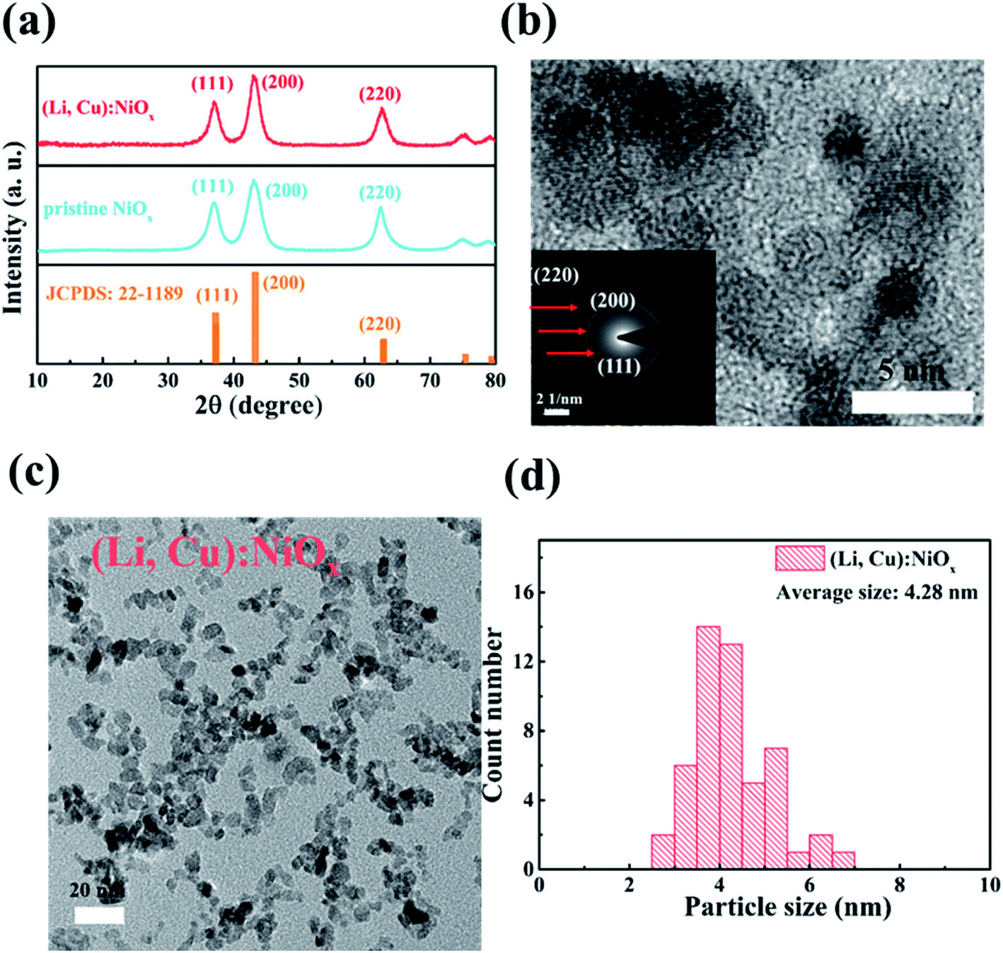 | ||
| Fig. 1 (a) XRD patterns of the as-synthesized of NiOx and (Li, Cu):NiOx NPs. (b) HRTEM image with the indexed SAED pattern of the as-synthesized (Li, Cu):NiOx NPs. (c) TEM image and (d) size distribution of the as-synthesized (Li, Cu):NiOx NPs. | ||
The XPS spectra of pristine NiOx and (Li, Cu):NiOx samples are shown in Fig. S2.† Both pristine and codoped NiOx films have typical peaks including the main peak at ∼854.1 eV, a shoulder at ∼855.5 eV, and a shake-up satellite peak at ∼861.2 eV.31,32 The main peak corresponds to Ni2+ in the standard Ni–O octahedral bonding configuration in cubic rock salt NiOx.33,34 The shoulder peak is ascribed to the Ni-vacancy induced Ni3+ ion,34–37 nickel hydroxides and oxyhydroxides,34,35 and nonlocal screening and surface states.31 Notably, in Fig. S2(b) and (c),† XPS peaks corresponding to Cu 2p2/3 (933.6 eV) and Li 1 s (55.9 eV) are clearly observed for the (Li, Cu):NiOx film, which are absent in the undoped NiOx film, revealing that Cu and Li are successfully incorporated into NiOx.38 Due to the Li and Cu doping, the obtained Ni3+/Ni2+ ratio of the (Li, Cu):NiOx film (1.68) is larger than that of undoped NiOx (1.57) which contributes to the increase of hole conductivity as further studied in a later section.
The surface morphologies of undoped NiOx and (Li, Cu):NiOx thin films on ITO glass were determined by top-view SEM and AFM as shown in Fig. 2(a)–(d). Notably, the (Li, Cu):NiOx film consists of small-sized crystalline grains and is uniform without pin holes (Fig. 2(a)). Moreover, 3D AFM images further confirm the closely packed and crack-free morphology of the (Li, Cu):NiOx film with a smaller root-mean-square roughness (RMS) of 3.09 nm (Fig. 2(c)) compared to the pristine NiOx film (4.00 nm; Fig. 2(d)). It is worth noting that the smooth and uniform surface of the (Li, Cu):NiOx film should be beneficial to the formation of high-quality perovskite films for realizing high-performance devices. Thus, the morphologies of perovskite layers on NiOx and the (Li, Cu):NiOx thin film were characterized by SEM as shown in Fig. S3(a) and (b).† It is found that all the perovskite films are homogeneous and densely packed. Notably, the perovskite crystal grains formed on (Li, Cu):NiOx (511 nm) show a larger grain size than those grown on NiOx (440 nm), as displayed in Fig. S3(c) and (d).† That is because the slightly larger contact angle (inset in Fig. S3(a) and (b)†) provides a non-wetting surface, favoring the suppression of heterogeneous nucleation39 and the promotion of the grain growth.12,40,41 Consequently, the (Li, Cu):NiOx based HTL favors the formation of a good quality perovskite film, which is one of the interesting properties for obtaining highly efficient PSCs.
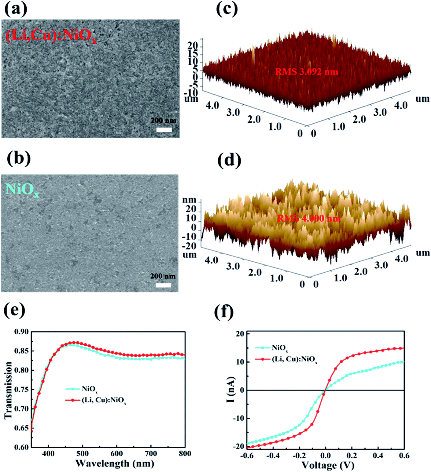 | ||
| Fig. 2 SEM images of (a) (Li, Cu):NiOx and (b) NiOx films on ITO glass. 3D AFM images: (c) (Li, Cu):NiOx and (d) NiOx films. (e) The transmittance spectra of NiOx and (Li, Cu):NiOx films on ITO glass. (f) I–V conducting curves of NiOx and (Li, Cu):NiOx films measured in the c-AFM mode. | ||
Electrical and optical properties are particularly important for realizing efficient HTLs. Firstly, we investigated the optical transmittance of NiOx and (Li, Cu):NiOx films coated on ITO glass as shown in Fig. 2(e). Interestingly, for the (Li, Cu):NiOx thin film, the transmittance reaches 87% at 460 nm, and shows an improvement over a large wavelength range from 500 to 800 nm than that of pristine NiOx. Furthermore, while light Li only doping does not change the transparency, the Cu doping will reduce the doping transmittance decreases as shown in Fig. S4† due to the d–d transition of Cu2+ in the crystalline environment of NiOx, which agrees with previous reports.34,42,43
We further study the effect of Li and Cu co-doping on the electrical conductivity of NiOx films by performing c-AFM measurements, as described in Fig. 2(f). From the I–V curves, a significantly higher current in the (Li, Cu):NiOx film (14.6 nA at a bias of 0.5 V) is clearly observed, indicating a dramatically increased conductivity compared to pristine NiOx (8 nA at a bias of 0.5 V). The increased ratio of Ni3+/Ni2+ supports the successful doping of Li and Cu as well as the improved hole conductivity, which is in good agreement with other reports (Fig. S5†).24,29,34,43–45 These results indicate the Li and Cu codoping strategy on NiOx could achieve significantly enhanced conductivity and keep high transparency, making it more suitable as an efficient HTL for achieving high-performance PSCs.
To explore the function of the (Li, Cu):NiOx film as the HTL, inverted PSCs with a structure of ITO/NiOx (or (Li, Cu):NiOx)/perovskite/PC61BM:C60/ZrAcac/Ag have been fabricated, where the corresponding energy level diagram is depicted in Fig. 3(a). The energy levels of ITO, perovskite, PC61BM:C60, ZrAcac, and Ag are collected from the literature,12,13,46 and NiOx or (Li, Cu):NiOx are obtained from UPS. It should be noted that zirconium acetylacetonate (ZrAcac) is inserted between the PC60BM:C60 and Ag cathode for efficiently extracting and transporting electrons. The cross-sectional view SEM image of the device configuration is shown in Fig. 3(b). Fig. 3(c) depicts the J–V curves of the champion devices based on pristine NiOx and (Li, Cu):NiOx under AM 1.5 G illumination. The (Li, Cu):NiOx based PSCs with an optimized thickness of 20 nm exhibited a short circuit current density (JSC) of 23.156 mA cm−2, an open-circuit voltage (VOC) of 1.11 V, and a fill factor (FF) of 0.81 to yield the best PCE of 20.83%, clearly outperforming the PSCs based on pristine NiOx as the HTL. The best-performing reference cell using pristine NiOx as the HTL gave a JSC of 22.02 mA cm−2, VOC of 1.09 V, FF of 0.75, and PCE of 17.91%. These values are comparable with those of a previous report on devices with the same structure.47 Thanks to the simultaneously enlarged transmittance and conductivity of the codoped HTL and the high-quality perovskite film with a larger grain size, the inverted PSCs displayed significantly enhanced JSC, FF, and PCE, which are also the highest among the reported NiOx based inverted PSCs, as shown in Table S1.† Additionally, the PSCs based on (Li, Cu):NiOx HTLs showed negligible J–V hysteresis in Fig. 3(d), which is better than that of NiOx based PSCs (Fig. S6†). The narrow distributions of the statistical photovoltaic parameters (JSC, VOC, FF, and PCEs) from 30 devices further confirm the reliability of performance improvement of (Li, Cu):NiOx-based PSCs (Fig. S7†). Fig. 3(e) shows the IPCE spectra of the champion devices based on NiOx and (Li, Cu):NiOx, where the integrated JSC from the IPCE over an AM 1.5 G spectrum approximately agrees with those obtained from J–V curves. In addition, the steady-state photocurrent output at the maximum power point over 200 s has been measured by applying a bias of 0.97, as shown in Fig. 3(f). There is no performance degradation under long illumination and a stable PCE of 20.24% for (Li, Cu):NiOx based PSCs was obtained, which is consistent with that of J–V measurement.
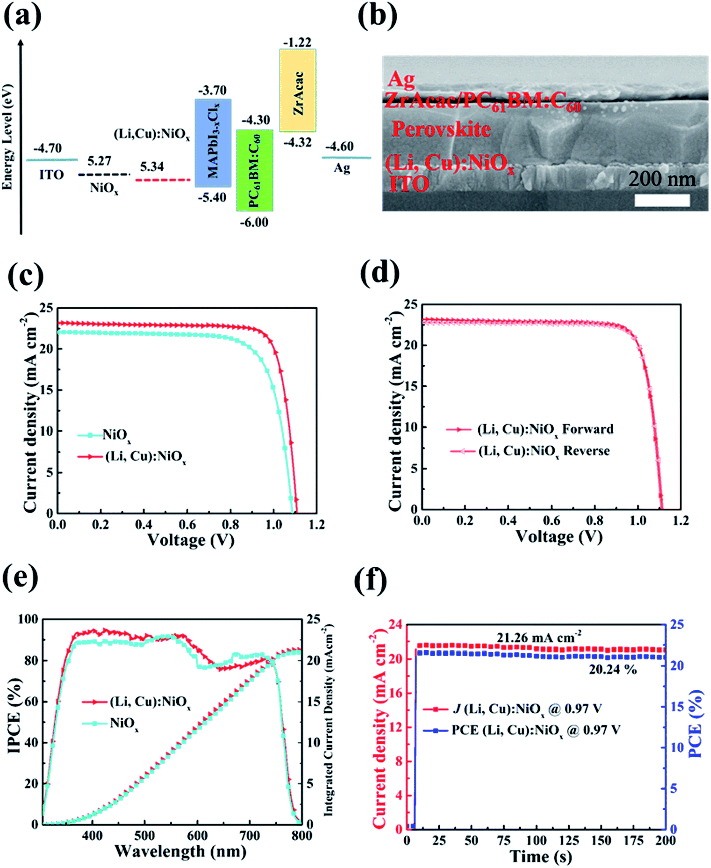 | ||
| Fig. 3 (a) Energy band level diagram of the various layers in inverted PSCs. (b) Cross-sectional SEM image of a complete perovskite device with (Li, Cu):NiOx films as the HTL. (c) J–V characteristics of the best NiOx and (Li, Cu):NiOx based PSCs measured under AM 1.5 G 100 mW cm−2 illumination. (d) J–V characteristics of (Li, Cu):NiOx based devices extracted from forward and reverse sweeping. (e) IPCE spectra and integrated JSC curves of the best NiOx and (Li, Cu):NiOx based PSCs. (f) Steady-state photocurrent output at the maximum power point of (Li, Cu):NiOx-based PSCs under continuous simulated AM 1.5 G illumination for 200 s. | ||
In order to explore the reasons for the improved performance by codoping with Li and Cu, we first compared the work function (WF) of NiOx and (Li, Cu):NiOx films by Kelvin-probe measurement. For each sample, 500 points are collected, as shown in Fig. S8.† The measured WF values are collected in Table S2.† The WF of the pristine NiOx film is determined to be 4.99 eV and shifted to 5.12 eV for (Li, Cu):NiOx. From the UPS and the corresponding energy level diagram in Fig. 4(a) and (b), Cu and Li codoping can cause energy band shifts and increase the work function,48 resulting in a favorable energy level alignment with the perovskite layer (−5.4 eV, Fig. 3(a)) and an enhanced hole extraction ability. In addition, the valence band (VB) shifted by about 0.02 eV closer to the Fermi energy level after Li and Cu codoping (Fig. 4(b)), showing enhanced p-type properties and improved film conductivity, which is consistent with the previous discussion.
 | ||
| Fig. 4 (a) UPS of the NiOx and (Li, Cu):NiOx films on ITO glass. (b) Energy level diagrams of the NiOx and (Li, Cu):NiOx films. (c) PL spectra for perovskite films on different substrates: glass (orange), pristine NiOx (black), and (Li, Cu):NiOx (red), respectively. (d) Time-resolved PL spectra of the perovskite film on NiOx and (Li, Cu):NiOx, respectively. (e) Nyquist plots of EIS spectra for the device with NiOx and (Li, Cu):NiOx as HTLs, respectively. | ||
To verify the charge extraction ability at the interface of HTL/perovskite, PL (Fig. 4(c)) and time-resolved PL (Fig. 4(d)) measurements of the perovskite layers deposited on NiOx, and (Li, Cu):NiOx films were conducted, respectively. It can clearly be observed that the (Li, Cu):NiOx HTL exhibits efficient PL quenching compared to that of pristine NiOx, illustrating a more favorable ohmic contact with the perovskite layer and obvious improvement of the hole extraction efficiency. Meanwhile, the TRPL profiles are shown in Fig. 4(d), where the PL lifetime is fitted by two-exponential decay.29,49 There is a decrease in the average PL lifetime for (Li, Cu):NiOx/perovskite (13 ns) as compared to pristine NiOx/perovskite (20 ns), which further validated a faster and more efficient hole extraction and transport ability at the (Li, Cu):NiOx/perovskite interface. Compared to NiOx, the more effective hole extraction and transport by the (Li, Cu):NiOx HTL from the perovskite active layer could be ascribed to the higher conductivity and increased work function, which would contribute to high JSC and FF values for (Li, Cu):NiOx based PSCs.
Charge transport and recombination ability can also be studied by EIS measurements, which are performed at a bias voltage of 0.9 V under dark conditions (Fig. 4(e)). The only one semicircle in the obtained Nyquist plot will be more likely related to the recombination resistance at the interface of the HTL/perovskite layer, where the larger the diameter is, the less the hole recombination at the interface. Compared to that of pristine NiOx based devices (1.3 KΩ), (Li, Cu):NiOx HTL based PSCs exhibit a larger charge recombination resistance (2.6 KΩ), illustrating less carrier recombination, which results in increased JSC and enhanced FF in the (Li, Cu):NiOx HTL based PSCs. As shown in the dark current–voltage curves of Fig. S9,† the lower dark current under negative bias in the (Li, Cu):NiOx HTL based PSCs illustrates that those PSCs based on the (Li, Cu):NiOx HTL exhibited a lower leakage current, reducing leakage-induced recombination that would improve the VOC.
Regarding the stability and reversibility of PSCs, the PCE of (Li, Cu):NiOx HTL based PSCs was characterized after one-month storage in a nitrogen-filled glovebox, as portrayed in Fig. 5. It is found that (Li, Cu):NiOx HTL-based devices exhibited excellent stable performance, retained 95% of initial PCE after 60 days of storage, implying the beneficial role of Cu and Li in preventing the undesired oxidation process on the NiOx surface.
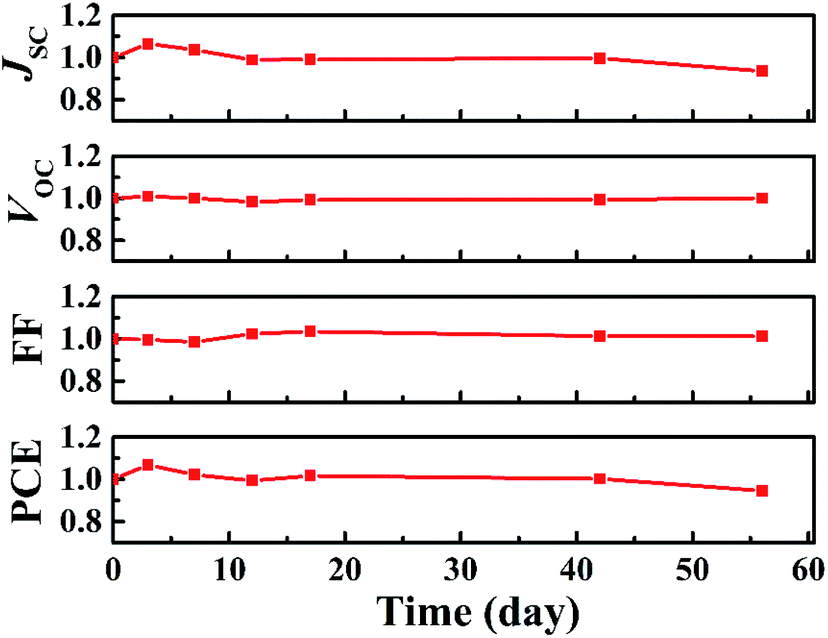 | ||
| Fig. 5 Photovoltaic performance parameter (JSC, VOC, FF, and PCE) of (Li, Cu):NiOx based PSCs as a function of storage time under an inert environment for almost 60 days. All devices were encapsulated and stored in a glove box. | ||
To demonstrate the feasibility of post-treatment free and room-temperature processed (Li, Cu):NiOx HTLs for application in flexible devices, we deposited a (Li, Cu):NiOx film onto an ITO-PET substrate to fabricate flexible PSCs. A photograph of a typical flexible device with an area of 0.08 cm2 is shown in Fig. S10(a).† Fig. S10(b)† illustrates the J–V curves of the champion flexible PSCs with a (Li, Cu):NiOx HTL (under AM 1.5 G illumination). The device exhibited a JSC of 22.02 mA cm−2, a VOC of 1.06, and a FF of 0.78, corresponding to the best PCE of 18.16%, which are comparable to those of the reported best flexible PSCs with inverted structures (Fig. S10(c)).† To the best of our knowledge, 18.2% is the highest PCE value attained for NiOx based flexible inverted PSCs. This result suggests that the (Li, Cu):NiOx HTL without any high-temperature treatment is compatible with the flexible substrate and shows a broad application prospect for the roll-to-roll scale-up fabrication process.
Another interesting feature of the (Li, Cu):NiOx films is that while only room temperature conditions are needed for forming efficiency HTLs, the films can tolerate a wide temperature range for the practical application of PSCs in a temperature changing environment. The J–V characteristics of PSCs using a (Li, Cu):NiOx HTL with different annealing temperatures are collected in Table S3.† Our results show that all the devices show similar performances for the co-doped (Li, Cu):NiOx HTL with annealing temperature up to 250 °C. With the annealing temperature further increasing to 300 °C, the PCE decreases, which is attributed to the decreased JSC and VOC. Our results demonstrate that the (Li, Cu):NiOx HTL in this work can function as an effective HTL without any post-treatment and offer wide temperature stability from room temperature up to 250 °C, which can contribute to the device stability during the fabrication and application of PSCs.
4. Conclusions
In this work, we have successfully demonstrated efficient HTLs by a simple room-temperature solution process without any treatment for high performance rigid and flexible PSCs. Particularly, a co-doped (Li, Cu):NiOx film simultaneously exhibits several interesting features of (1) improved electrical conductivity, (2) enhanced optical transmittance, (3) high quality (compact and uniform), and (4) favoring large grain-size perovskite film formation. The PCE of PSCs based on (Li, Cu):NiOx HTLs improved by 15% as compared to the case of pristine NiOx and reached a promising value of 20.8% on rigid substrates and 18.2% on flexible substrates. While an effective co-doped (Li, Cu):NiOx HTL is formed at room temperature, the high performance can sustain annealing temperature up to 250 °C. Meanwhile, the PSCs exhibit excellent stability, with 95% of the original efficiency remaining after 1000 h of storage under ambient conditions. This work provides a promising route to realize highly efficient and stable rigid and flexible PSCs using abundant low-cost inorganic HTLs.Conflicts of interest
The authors declare no competing financial interests.Acknowledgements
This work was supported by the University Grant Council of the University of Hong Kong (Grant# 201811159147, and Research Equipment Fund), the General Research Fund (Grant 17204117, 17200518, 17201819, and 17211220), and the Collaborative Research Fund (C5037-18G) from the Research Grants Council (RGC), and the Environment and Conservation Fund (ECF Project 64/2018) of Hong Kong Special Administrative Region, China.References
- N. J. Jeon, J. H. Noh, Y. C. Kim, W. S. Yang, S. Ryu and S. I. Seok, Nat. Mater., 2014, 13, 897–903 CrossRef CAS.
- Q. Dong, Y. Fang, Y. Shao, P. Mulligan, J. Qiu, L. Cao and J. Huang, Science, 2015, 347, 967–970 CrossRef CAS.
- H. Oga, A. Saeki, Y. Ogomi, S. Hayase and S. Seki, J. Am. Chem. Soc., 2014, 136, 13818–13825 CrossRef CAS.
- C. Wehrenfennig, G. E. Eperon, M. B. Johnston, H. J. Snaith and L. M. Herz, Adv. Mater., 2014, 26, 1584–1589 CrossRef CAS.
- A. Kojima, K. Teshima, Y. Shirai and T. Miyasaka, J. Am. Chem. Soc., 2009, 131, 6050–6051 CrossRef CAS.
- National Renewable Energy Laboratory, NREL Efficiency Chart, 2019, https://www.nrel.gov/pv/assets/pdfs/best-research-cell-efficiencies.20190128.pdf Search PubMed.
- P. Qin, S. Tanaka, S. Ito, N. Tetreault, K. Manabe, H. Nishino, M. K. Nazeeruddin and M. Gratzel, Nat. Commun., 2014, 5, 3834 CrossRef CAS.
- Z. Zhu, Y. Bai, T. Zhang, Z. Liu, X. Long, Z. Wei, Z. Wang, L. Zhang, J. Wang, F. Yan and S. Yang, Angew. Chem., Int. Ed., 2014, 53, 12571–12575 CAS.
- S. S. Shin, W. S. Yang, J. H. Noh, J. H. Suk, N. J. Jeon, J. H. Park, J. S. Kim, W. M. Seong and S. I. Seok, Nat. Commun., 2015, 6, 7410 CrossRef CAS.
- C. Zuo and L. Ding, Small, 2015, 11, 5528–5532 CrossRef CAS.
- H. Zhang, J. Cheng, F. Lin, H. He, J. Mao, K. S. Wong, A. K. Jen and W. C. Choy, ACS Nano, 2016, 10, 1503–1511 CrossRef CAS.
- D. Ouyang, J. Xiao, F. Ye, Z. Huang, H. Zhang, L. Zhu, J. Cheng and W. C. H. Choy, Adv. Energy Mater., 2018, 8, 1702722 CrossRef.
- H. Zhang, H. Wang, H. Zhu, C.-C. Chueh, W. Chen, S. Yang and A. K. Y. Jen, Adv. Energy Mater., 2018, 8, 1702762 CrossRef.
- D. Ouyang, Z. Huang and W. C. H. Choy, Adv. Funct. Mater., 2019, 29, 1804660 CrossRef.
- Z. Huang, D. Ouyang, C. J. Shih, B. Yang and W. C. H. Choy, Adv. Energy Mater., 2020, 10, 1900903 CrossRef CAS.
- M. Hajizadeh-Oghaz, Ceram. Int., 2019, 45, 6994–7000 CrossRef CAS.
- H. Chen, W. Zhu, Z. Zhang, W. Cai and X. Zhou, J. Alloys Compd., 2019, 771, 649–657 CrossRef CAS.
- M. Vasilopoulou, N. Kelaidis, E. Polydorou, A. Soultati, D. Davazoglou, P. Argitis, G. Papadimitropoulos, D. Tsikritzis, S. Kennou, F. Auras, D. G. Georgiadou, S. G. Christopoulos and A. Chroneos, Sci. Rep., 2017, 7, 17839 CrossRef.
- A. Ioakeimidis, I. T. Papadas, D. Tsikritzis, G. S. Armatas, S. Kennou and S. A. Choulis, APL Mater., 2019, 7, 021101 CrossRef.
- S. Wang, B. Zhang, D. Feng, Z. Lin, J. Zhang, Y. Hao, X. Fan and J. Chang, J. Mater. Chem. C, 2019, 7, 9270–9277 RSC.
- B. Zhang, Z. Song, J. Jin, W. Bi, H. Li, C. Chen, Q. Dai, L. Xu and H. Song, J. Colloid Interface Sci., 2019, 553, 14–21 CrossRef CAS.
- J. Tian, J. Zhang, X. Li, B. Cheng, J. Yu and W. Ho, Sol. RRL, 2020, 4, 2000090 CrossRef CAS.
- D. Hou, J. Zhang, X. Gan, H. Yuan, L. Yu, C. Lu, H. Sun, Z. Hu and Y. Zhu, J. Colloid Interface Sci., 2020, 559, 29–38 CrossRef CAS.
- M. H. Liu, Z. J. Zhou, P. P. Zhang, Q. W. Tian, W. H. Zhou, D. X. Kou and S. X. Wu, Opt. Express, 2016, 24, A1349–A1359 CrossRef CAS.
- X. Xia, Y. Jiang, Q. Wan, X. Wang, L. Wang and F. Li, ACS Appl. Mater. Interfaces, 2018, 10, 44501–44510 CrossRef CAS.
- F. Jiang, W. C. Choy, X. Li, D. Zhang and J. Cheng, Adv. Mater., 2015, 27, 2930–2937 CrossRef CAS.
- Q. He, K. Yao, X. Wang, X. Xia, S. Leng and F. Li, ACS Appl. Mater. Interfaces, 2017, 9, 41887–41897 CrossRef CAS.
- K. H. Kim, C. Takahashi, Y. Abe and M. Kawamura, Optik, 2014, 125, 2899–2901 CrossRef CAS.
- H. S. Kim, J. Y. Seo, H. Xie, M. Lira-Cantu, S. M. Zakeeruddin, M. Gratzel and A. Hagfeldt, ACS Omega, 2017, 2, 9074–9079 CrossRef CAS.
- R. Kaneko, T. H. Chowdhury, G. Wu, M. E. Kayesh, S. Kazaoui, K. Sugawa, J.-J. Lee, T. Noda, A. Islam and J. Otsuki, Sol. Energy, 2019, 181, 243–250 CrossRef CAS.
- S. Seo, I. J. Park, M. Kim, S. Lee, C. Bae, H. S. Jung, N. G. Park, J. Y. Kim and H. Shin, Nanoscale, 2016, 8, 11403–11412 RSC.
- Z. Qiu, H. Gong, G. Zheng, S. Yuan, H. Zhang, X. Zhu, H. Zhou and B. Cao, J. Mater. Chem. C, 2017, 5, 7084–7094 RSC.
- S. W. T. Jesse, R. Manders, M. J. Hartel, T. H. Lai, S. Chen, C. M. Amb, J. R. Reynolds and F. So, Adv. Funct. Mater., 2013, 23, 2993–3001 CrossRef.
- W. Chen, Y. Wu, J. Fan, A. B. Djurišić, F. Liu, H. W. Tam, A. Ng, C. Surya, W. K. Chan, D. Wang and Z.-B. He, Adv. Energy Mater., 2018, 8, 1703519 CrossRef.
- J. Cui, F. Meng, H. Zhang, K. Cao, H. Yuan, Y. Cheng, F. Huang and M. Wang, ACS Appl. Mater. Interfaces, 2014, 6, 22862–22870 CrossRef CAS.
- K. C. Wang, P. S. Shen, M. H. Li, S. Chen, M. W. Lin, P. Chen and T. F. Guo, ACS Appl. Mater. Interfaces, 2014, 6, 11851–11858 CrossRef CAS.
- S. S. Mali and C. K. Hong, Nanoscale, 2016, 8, 10528–10540 RSC.
- J. Jang, S. Chung, H. Kang and V. Subramanian, Thin Solid Films, 2016, 600, 157–161 CrossRef CAS.
- C. Bi, Q. Wang, Y. Shao, Y. Yuan, Z. Xiao and J. Huang, Nat. Commun., 2015, 6, 7747 CrossRef CAS.
- B. Yang, D. Ouyang, Z. Huang, X. Ren, H. Zhang and W. C. H. Choy, Adv. Funct. Mater., 2019, 29, 1902600 CrossRef.
- P.-W. Liang, C.-C. Chueh, S. T. Williams and A. K. Y. Jen, Adv. Energy Mater., 2015, 5, 1402321 CrossRef.
- J. W. Jung, C. C. Chueh and A. K. Jen, Adv. Mater., 2015, 27, 7874–7880 CrossRef CAS.
- S. C. Chen, T. Y. Kuo, Y. C. Lin and H. C. Lin, Thin Solid Films, 2011, 519, 4944–4947 CrossRef CAS.
- J. Zheng, L. Hu, J. S. Yun, M. Zhang, C. F. J. Lau, J. Bing, X. Deng, Q. Ma, Y. Cho, W. Fu, C. Chen, M. A. Green, S. Huang and A. W. Y. Ho-Baillie, ACS Appl. Energy Mater., 2018, 1, 561–570 CrossRef CAS.
- X. Wan, Y. Jiang, Z. Qiu, H. Zhang, X. Zhu, I. Sikandar, X. Liu, X. Chen and B. Cao, ACS Appl. Energy Mater., 2018, 1, 3947–3954 CrossRef CAS.
- Y. Zhao, H. Zhang, X. Ren, H. L. Zhu, Z. Huang, F. Ye, D. Ouyang, K. W. Cheah, A. K. Y. Jen and W. C. H. Choy, ACS Energy Lett., 2018, 3, 2891–2898 CrossRef CAS.
- S. Yue, K. Liu, R. Xu, M. Li, M. Azam, K. Ren, J. Liu, Y. Sun, Z. Wang, D. Cao, X. Yan, S. Qu, Y. Lei and Z. Wang, Energy Environ. Sci., 2017, 10, 2570–2578 RSC.
- S. Xiao, F. Xu, Y. Bai, J. Xiao, T. Zhang, C. Hu, X. Meng, H. Tan, H. P. Ho and S. Yang, Sol. RRL, 2018, 3, 1800278 CrossRef.
- Y. Li, L. Meng, Y. M. Yang, G. Xu, Z. Hong, Q. Chen, J. You, G. Li, Y. Yang and Y. Li, Nat. Commun., 2016, 7, 10214 CrossRef CAS.
Footnote |
| † Electronic supplementary information (ESI) available. See DOI: 10.1039/d0ta05873d |
| This journal is © The Royal Society of Chemistry 2021 |