
Sub-5 nm homeotropically aligned columnar structures of hybrids constructed by porphyrin and oligo(dimethylsiloxane)†
Weilu
Yang
 a,
Dong
Liu
a,
Longfei
Luo
a,
Peiyun
Li
b,
Yun
Liu
a,
Zhihao
Shen
*a,
Ting
Lei
b,
Huai
Yang
b,
Xing-He
Fan
*a and
Qi-Feng
Zhou
a
a,
Dong
Liu
a,
Longfei
Luo
a,
Peiyun
Li
b,
Yun
Liu
a,
Zhihao
Shen
*a,
Ting
Lei
b,
Huai
Yang
b,
Xing-He
Fan
*a and
Qi-Feng
Zhou
a
aBeijing National Laboratory for Molecular Sciences, Key Laboratory of Polymer Chemistry and Physics of Ministry of Education, Center for Soft Matter Science and Engineering, and College of Chemistry and Molecular Engineering, Peking University, Beijing 100871, China. E-mail: zshen@pku.edu.cn; fanxh@pku.edu.cn
bKey Laboratory of Polymer Chemistry and Physics of Ministry of Education, and School of Materials Science and Engineering, Peking University, Beijing 100871, China
First published on 27th November 2021
Abstract
A series of tetraphenylporphyrin-based thermotropic liquid crystals containing oligo(dimethylsiloxane) were synthesized. These disc–coil hybrids form ordered nanostructures with periodic sizes on the sub-5 nm scale, including oblique columnar, lamellar, and hexagonal columnar phases. Films with sub-5 nm line patterns and homeotropically aligned columnar structures can be obtained by substrate-induced self-assembly.
Following Moore's law,1 the device feature size keeps reducing to the sub-5 nm length scale.2 The formation of a perfect array with small-sized features and long–range order is one of the crucial challenges in nanotechnology.3 Liquid crystals (LCs) with highly ordered nanostructures are promising building blocks to create nanotemplates.4 They have attracted more and more attention owing to their advantageous properties, including uniform small feature sizes (<10 nm), various highly ordered structures, easily oriented character, and shorter stabilization times when compared to block copolymers (BCPs).4
Oligo(dimethylsiloxane) (ODMS), composed of a discrete siloxane main chain and methyl substituents, are a kind of attractive etch mask precursor, which can transform into inorganic silicon oxide via oxygen plasma oxidation.5 They have low surface energy and high chemical incompatibility with most organic components.6,7 By covalently attaching ODMS to various aromatic cores such as naphthalenediimides,8 azobenzene,9 and other aromatic cores, long-range ordered nanostructures including cubic, hexagonal columnar (Colh),10 rectangular columnar, gyroid,11 and lamellar (Lam)12 phases with relatively small feature sizes were constructed.13–15 Moreover, long-range ordered line patterns on silicon substrates with sub-5 nm feature sizes were obtained by taking advantage of the photo-response of azobenzene and directed self-assembly (DSA) in prefabricated nanotrenches.4,6,16 However, thin films with vertically aligned structures constructed by ODMS-based LCs are difficult to obtain owing to the intrinsic surface energy mismatch between ODMS and LC cores,6 and completely vertically oriented structures have not been reported, although obtaining such structures is a very challenging and critical step in preparing nanotemplates.6,16
Porphyrins with large conjugated structures can easily form supramolecular columnar structures by π–π stacking interactions.17–20 In addition, porphyrin cores have suitable polarity, and homeotropic alignment or parallel alignment of porphyrin-based disc–coil LCs can be easily regulated by varying the surface properties of substrates, leading to supramolecular columns with either parallel or vertical orientation.21–24
Considering these advantages of porphyrin and ODMS, we covalently link disc-like tetraphenylporphyrin (TPP) and four ODMS coil chains together to create a series of new hybrid LCs, TPP-4Sin (n represents the number of repeating units in ODMS, and n = 3, 7, 11). Scheme 1 shows the synthetic route, and specific synthetic procedures are described in the ESI.† Chemical structures of the LCs were confirmed by 1H NMR (Fig. S1, S3 and S5, ESI†), 13C NMR (Fig. S2, S4 and S6, ESI†), and matrix-assisted laser desorption/ionization time-of-flight (MALDI-TOF) mass spectra (Fig. S7, ESI†). The introduction of the porphyrin core and peripheral ester bonds makes it possible to regulate the orientation of the self-assembled structures.
 | ||
| Scheme 1 Synthetic route of TPP-4Si3, TPP-4Si7, and TPP-4Si11. | ||
Thermogravimetric analysis (TGA) results (Fig. S8, ESI†) show that all these LCs have excellent thermal stabilities with decomposition temperatures at 5% weight loss over 390 °C. Differential scanning calorimetry (DSC) (Fig. S9, ESI†) and polarized light microscopy (PLM) (Fig. S10, ESI†) were used to determine their phase transition temperatures, with results summarized in Table S1 (ESI†).
The self-assembled structures of these LCs in bulk were studied by in situ temperature-dependent wide-angle X-ray scattering (WAXS). As shown in Fig. 1a, at ambient temperature, five diffraction peaks with q = 1.81, 2.18, 4.32, 3.62, and 4.53 nm−1 are present in the WAXS profile of TPP-4Si3. Presumably, these peaks can be indexed as (10), (01), (20), (02), and (21) diffractions of an oblique columnar (Colob) structure with a = 3.53 nm, b = 2.94 nm, and γ = 100.8°. A schematic packing model is shown in Fig. 1b. The rigid aromatic porphyrin discs (red in the model) are arranged to form columnar arrays of the Colob structure, while the space between the cylinders was filled by flexible ODMS chains (blue in the model). The peak related to π–π stacking could be found at q = 18.99 nm−1 (Fig. S11, ESI†), indicating the relatively ordered stacking of the porphyrin cores with a distance of 0.33 nm. At 240 °C, all these peaks disappear; thus, the sample turns isotropic.
 | ||
| Fig. 1 Temperature-dependent WAXS profiles and schematic models of TPP-4Si3 ((a): the halo at q = 4.25 nm−1 is attributed to the scattering of the Kapton tape supporting the sample; (b): Colob phase), TPP-4Si7 ((c and d): Lam phase), and TPP-4Si11 ((e and f): Colh phase, with red plates and blue lines representing rigid TPP cores and ODMS chains, respectively). | ||
For TPP-4Si7, only a primary diffraction peak with q = 1.49 nm−1 is observed from the WAXS profile (Fig. 1c) of the bulk sample at ambient temperature, and the d-spacing value is 4.11 nm. In the integral curve of grazing-incidence wide-angle X-ray diffraction (GI-WAXD) from a thermally annealed thin-film sample, a secondary diffraction peak is observed at q = 2.97 nm−1, suggesting the formation of a Lam phase. The peak related to π–π stacking of the porphyrin cores cannot be observed in the high-angle region (Fig. S12. ESI†), revealing that the packing of rigid cores in the supramolecular sheets is relatively disordered. A schematic packing model of the Lam structure is given in Fig. 1d. The porphyrin cores are aligned to form layers, while the ODMS chains fill in the other sublayers in an interdigitated manner. At 150 °C, the diffraction peak turns into a diffused scattering halo; in combination with the PLM results, TPP-4Si7 becomes isotropic.
As shown in Fig. 1e, at ambient temperature, three diffraction peaks with q = 1.44, 2.51, and 2.83 nm−1 having a q ratio of 1![[thin space (1/6-em)]](https://www.rsc.org/images/entities/char_2009.gif) :31/2:2 are observed in the WAXS profile (Fig. 3d) of TPP-4Si11. These three peaks can be indexed as (10), (11), and (20) diffractions of a Colh structure with a cell parameter a of 4.96 nm. The peak related to π–π stacking of the aromatic porphyrin cores cannot be observed (Fig. S13, ESI†), revealing the relatively disordered packing of the rigid discs in the supramolecular columns. The schematic packing model of the Colh structure is given in Fig. 1f. Similar to TPP-4Si7, when the temperature is increased to 150 °C, the primary diffraction peak turns into a diffused scattering halo and the secondary peak disappears, demonstrating that it becomes isotropic.
:31/2:2 are observed in the WAXS profile (Fig. 3d) of TPP-4Si11. These three peaks can be indexed as (10), (11), and (20) diffractions of a Colh structure with a cell parameter a of 4.96 nm. The peak related to π–π stacking of the aromatic porphyrin cores cannot be observed (Fig. S13, ESI†), revealing the relatively disordered packing of the rigid discs in the supramolecular columns. The schematic packing model of the Colh structure is given in Fig. 1f. Similar to TPP-4Si7, when the temperature is increased to 150 °C, the primary diffraction peak turns into a diffused scattering halo and the secondary peak disappears, demonstrating that it becomes isotropic.
The schematic phase diagram of these LCs is depicted in Fig. S14 (ESI†). The Lam-to-Colh phase transition is similar to the trend in the self-assembly of BCPs, which is attributed to the change of the coil volume fraction (fcoil). TPP-4Si7 with fcoil = 0.63 that is asymmetric but more or less close to 0.5 assembles into a Lam structure. TPP-4Si11 with fcoil = 0.72 that is more asymmetric forms a Colh structure.
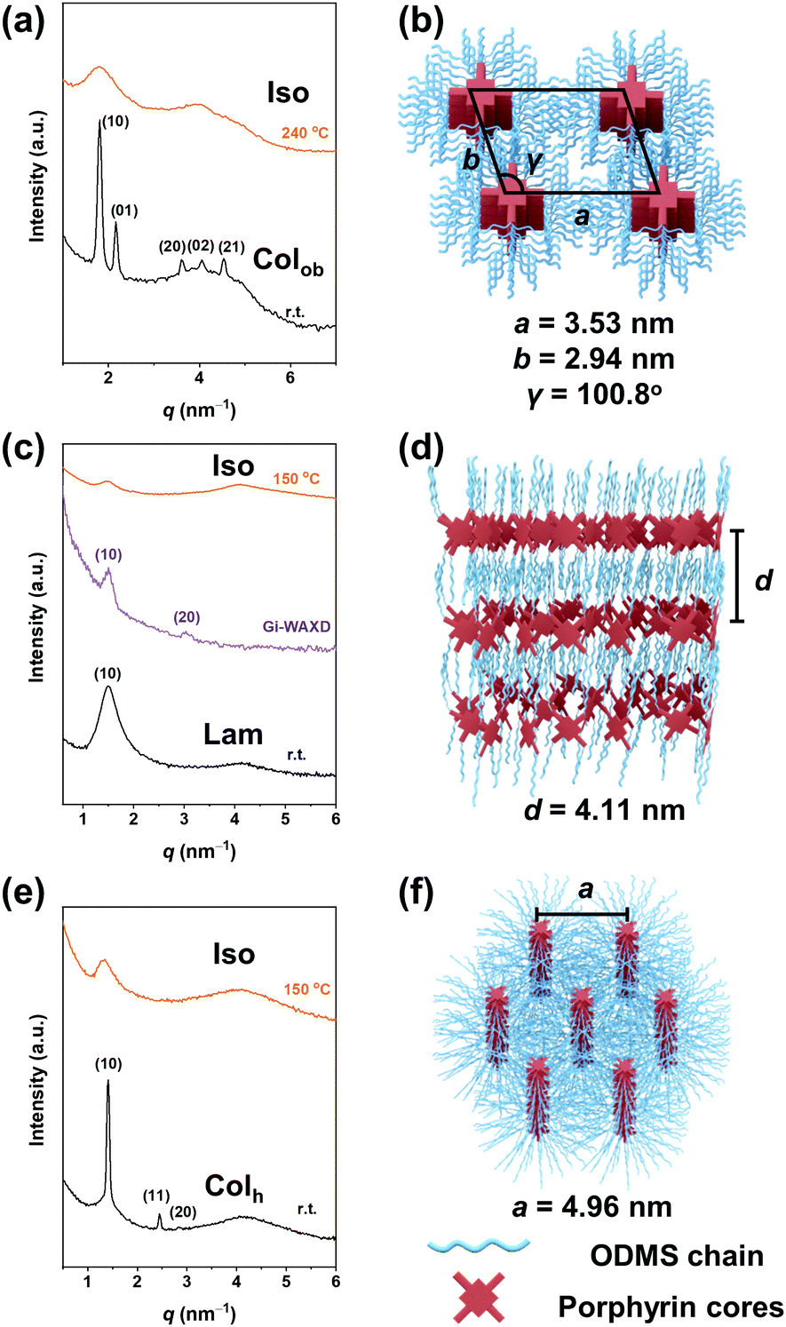
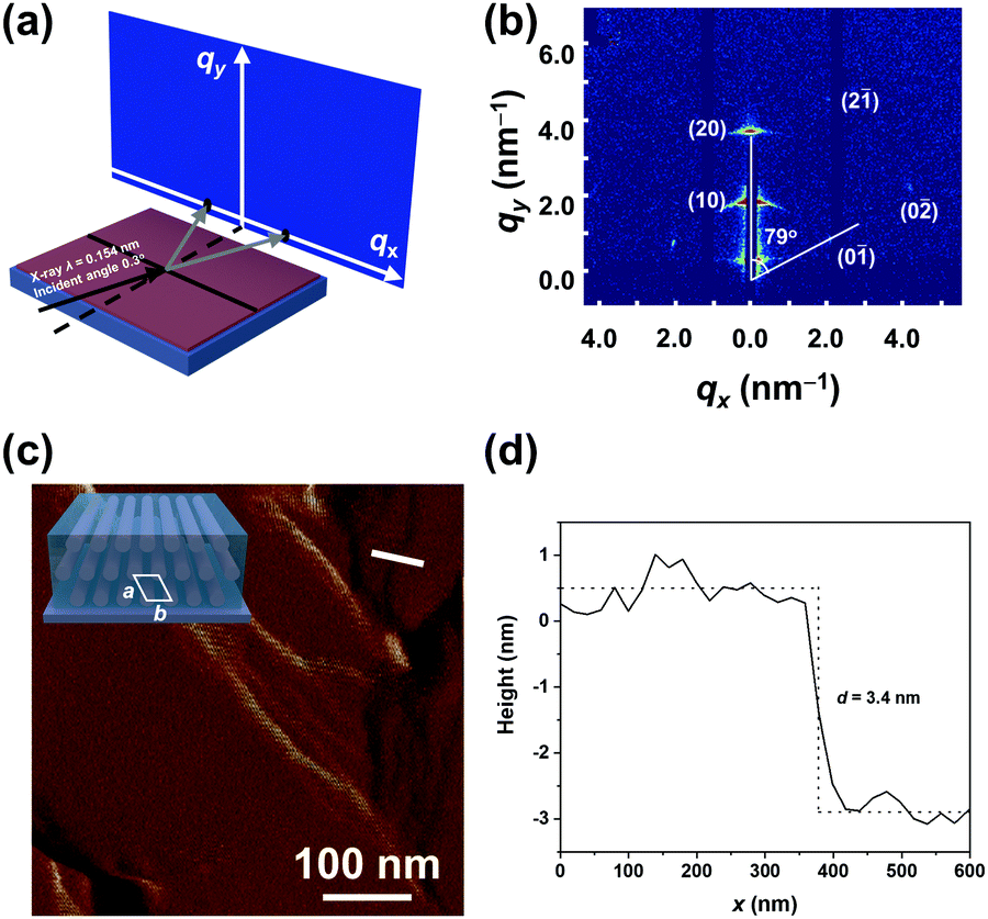
Based on the understanding of their self-assembled structures in bulk, thin-film self-assembly was also studied. In order to enhance the compatibility between the substrate and LCs, a Si wafer was modified with a polydimethylsiloxane (PDMS, Mn = 5000 Da) polymer brush in advance (detailed modification method is described in the ESI†). The success of the modification was verified by the water contact angle measurements (Fig. S15a, ESI†). Then uniform thin films with a thickness of about 82 nm (Fig. S15b, ESI†) were prepared and annealed (detailed method is described in the ESI†). Their thin-film self-assembled structures were characterized using GI-WAXD and tapping-mode AFM. Fig. 2a is a schematic illustration of the GI-WAXD experiment. For the thin film of TPP-4Si3, the GI-WAXD pattern (Fig. 2b) shows that the (10) and (20) diffractions are located along the qy direction, and the (01) and (02) diffractions are located in the quadrants with an angle of 79° to qy. In addition, the (21) plane can also be well assigned. These results prove the assignment of the Colob structure from the WAXS profile at ambient temperature mentioned previously. An AFM phase image (Fig. 2c) shows flat sheets with a constant height difference of ca. 3.4 nm between two consecutive layers on the basis of the cross-sectional scanning curve (Fig. 2d). This value is consistent with the d-spacing of the (10) plane (3.47 nm) of the Colob phase in bulk. These results indicate that the columns of the Colob structure have a parallel orientation with respect to the Si substrate and the normal direction of the (10) plane is perpendicular to the Si substrate. The schematic model of the thin-film self-assembled structure is shown in the upper left of Fig. 2c, where the red columns represent the porphyrin cores and the blue matrix represents the ODMS chains. For the thin film of TPP-4Si7, the GI-WAXD pattern (Fig. 3a) shows that the (10) and (20) diffractions are located along the qy direction. AFM height images (Fig. 3b) of the thin-film surface show flat sheets with a constant height difference of ca. 4.1 nm between two consecutive layers according to the cross-sectional scanning curve (Fig. S16, ESI†), in agreement with the spacing (d = 4.11 nm) of the Lam phase in bulk. These results demonstrate the parallel orientation of the Lam phase relative to the Si substrate.
 | ||
| Fig. 2 Schematic illustration of the GI-WAXD experiment (a); GI-WAXD pattern (b) and AFM phase image (c) and cross-sectional scanning curve from the AFM phase image (d) of the thin film of TPP-4Si3. | ||
For the thin film of TPP-4Si11, the (10) diffraction of the Colh structure in the Gi-WAXD pattern (Fig. 3c) is along the median direction. And highly ordered line features with a spacing of ca. 4.9 nm measured from the cross-sectional scanning curve (Fig. S17, ESI†) are observed from the tapping-mode AFM phase image (Fig. 3d). The contrast in the AFM phase images originates from the varying hardness of the flexible ODMS coils and the rigid TPP moieties in tapping mode (TPP units = light, ODMS coils = dark). The spacing corresponds to the lattice parameter a (4.96 nm) of the Colh phase from bulk WAXS data. Moreover, the line patterns can be found clearly in large areas with a few defects (Fig. S18, ESI†). All these results illustrate that the bulk self-assembled structure is well retained in the thin film with parallel orientation. Owing to the extremely low surface energy (γPDMS = 20.5 mN·m−1) of ODMS coils, an ODMS wetting layer in the air interface should form for all these three structures. Therefore, the cylindrical structures in both Colob and Colh are buried underneath the wetting layer.4
 | ||
| Fig. 3 GI-WAXD pattern (a) and AFM height image (b) of TPP-4Si7 thin films; GI-WAXD pattern (c) and AFM phase image ((d); the upper right inset is the corresponding FFT pattern) of TPP-4Si11 thin films. | ||
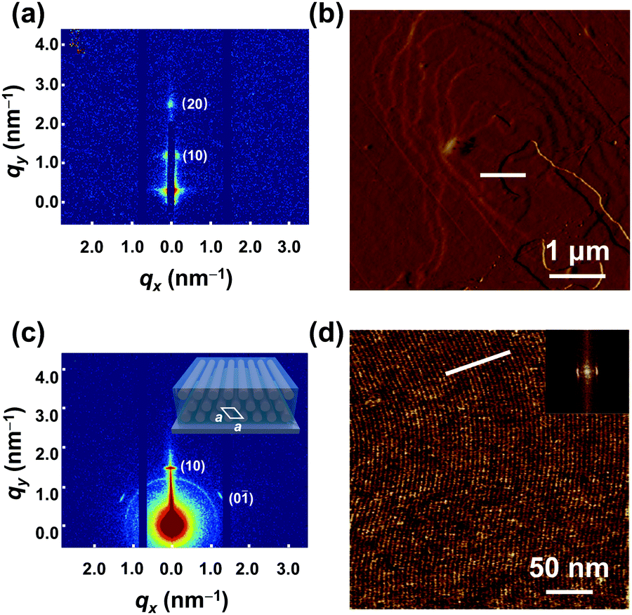
We further investigated the homeotropic alignment of TPP-4Si11 both in a 1 μm-thick glass cell and on the surface of a Si wafer. By controlling the corresponding annealing process, the supramolecular columns formed by the intermolecular π–π stacking of porphyrin can be aligned spontaneously perpendicular to the substrate. In order to obtain the vertically aligned structure in the glass cell, a cell with a 1 μm thickness was prepared first (details are described in the ESI†). TPP-4Si11 can be capillary-filled into the cell when being heated to the isotropic state. The sample in the cell was slowly cooled to ambient temperature at a cooling rate of 0.2 °C min−1. The PLM micrograph (Fig. 4a) is almost completely dark between crossed polarizers, indicating that the columns are perpendicularly aligned with respect to the substrates, i.e., in a homeotropic alignment. The dark areas represent homeotropic alignment, and the bright domains appear when the porphyrin planes are inclined to the substrate. The six-fold two-dimensional (2D) WAXD pattern obtained from the optically dark domain also confirms the homeotropic alignment (Fig. 4b).
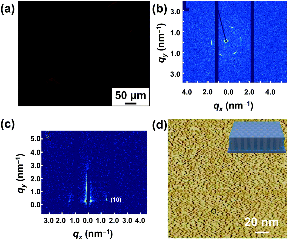 | ||
| Fig. 4 PLM micrograph (a) and 2D WAXD pattern from the homeotropic monodomain (b) of TPP-4Si11 in a 1 μm thick glass cell; GI-WAXD pattern (c) and AFM phase image (d) of homeotropic TPP-4Si11 thin film. | ||
The solvent annealing process for the vertical alignment on a Si substrate was performed according to Jung et al.'s publication.25 The preparation and annealing details of homeotropically-aligned TPP-4Si11 thin films are described in the experimental section of ESI.† The GI-WAXD pattern with two reflections along the qx direction (Fig. 4c) and the tapping-mode AFM phase image (Fig. 4d) confirm the perpendicularly aligned supramolecular columns on the Si wafer. Furthermore, plasma etching experiments were applied to a perpendicularly aligned thin film of TPP-4Si11. Hole structures were observed in the AFM height image obtained by using the Scanasyst mode (Fig. S19a, ESI†). The GI-WAXD pattern remains unchanged after etching (Fig. S19b, ESI†), indicating that the self-assembled structure is maintained during etching.
In conclusion, the disc−coil hybrid LCs with covalently linked porphyrin and ODMS chains having variable numbers of siloxane repeating units were designed and synthesized. Colob, Lam, and Colh self-assembled structures with periodic sizes of less than 5 nm were obtained. These structures can be well transferred onto thin films with parallel orientation by simple thermal annealing on a PDMS-modified Si wafer. In addition, the well-ordered Colh structure of TPP-4Si11 can be perpendicularly aligned by thermal annealing in a 1 μm-thick glass cell or by solvent annealing under PVA-coated double-sandwiched confinement.
This work was supported by the National Key R&D Program of China (Grant 2018YFB0703702) and the National Natural Science Foundation of China (Grants 51725301, 21674004, and 51921002). The authors also thank Prof. Jian Pei for allowing the use of the LCCP-6A plasma etching system.
Conflicts of interest
There are no conflicts to declare.Notes and references
- G. E. Moore, Electronics, 1965, 38, 114–117 Search PubMed.
- Y. Rokhlenko, K. Kawamoto, J. A. Johnson and C. O. Osuji, Macromolecules, 2018, 51, 3680–3690 CrossRef CAS.
- L.-Y. Shi, C. Yin, B. Zhou, W. Xia, L. Weng and C. A. Ross, Macromolecules, 2021, 54, 1657–1664 CrossRef CAS.
- K. Nickmans and A. P. H. J. Schenning, Adv. Mater., 2018, 30, 1703713 CrossRef.
- B. van Genabeek, B. F. M. de Waal, M. M. J. Gosens, L. M. Pitet, A. R. A. Palmans and E. W. Meijer, J. Am. Chem. Soc., 2016, 138, 4210–4218 CrossRef CAS PubMed.
- K. Nickmans, G. M. Bögels, C. Sánchez-Somolinos, J. N. Murphy, P. Leclère, I. K. Voets and A. P. H. J. Schenning, Small, 2017, 13, 1701043 CrossRef.
- K. Nickmans, R. C. P. Verpaalen, J. N. Murphy and A. P. H. J. Schenning, J. Mater. Chem. C, 2018, 6, 3042–3046 RSC.
- J. A. Berrocal, R. H. Zha, B. F. M. de Waal, J. A. M. Lugger, M. Lutz and E. W. Meijer, ACS Nano, 2017, 11, 3733–3741 CrossRef CAS.
- R. H. Zha, G. Vantomme, J. A. Berrocal, R. Gosens, B. de Waal, S. Meskers and E. W. Meijer, Adv. Funct. Mater., 2018, 28, 1703952 CrossRef.
- R. H. Zha, B. F. M. de Waal, M. Lutz, A. J. P. Teunissen and E. W. Meijer, J. Am. Chem. Soc., 2016, 138, 5693–5698 CrossRef CAS PubMed.
- W. Yang, W. Zhang, L. Luo, X. Lyu, A. Xiao, Z. Shen and X.-H. Fan, Chem. Commun., 2020, 56, 10341–10344 RSC.
- K. Nickmans, S. O. Jansma, D. Hey, G. Velpula, J. Teyssandier, S. De Feyter and A. P. H. J. Schenning, Helv. Chim. Acta, 2018, 101, e1800130 CrossRef.
- J. A. Berrocal, J. Teyssandier, O. J. G. M. Goor, S. De Feyter and E. W. Meijer, Chem. Mater., 2018, 30, 3372–3378 CrossRef CAS PubMed.
- M. H. C. van Son, A. M. Berghuis, F. Eisenreich, B. de Waal, G. Vantomme, J. Gómez Rivas and E. W. Meijer, Adv. Mater., 2020, 32, 2004775 CrossRef CAS PubMed.
- B. van Genabeek, B. F. M. de Waal, B. Ligt, A. R. A. Palmans and E. W. Meijer, ACS Macro Lett., 2017, 6, 674–678 CrossRef CAS.
- K. Nickmans, J. N. Murphy, B. de Waal, P. Leclère, J. Doise, R. Gronheid, D. J. Broer and A. P. H. J. Schenning, Adv. Mater., 2016, 28, 10068–10072 CrossRef CAS.
- M. Shirakawa, S.-i. Kawano, N. Fujita, K. Sada and S. Shinkai, J. Org. Chem., 2003, 68, 5037–5044 CrossRef CAS PubMed.
- W. Liu, Y. Shi, T. Shi, G. Liu, Y. Liu, C. Wang and W. Zhang, Liq. Cryst., 2003, 30, 1255–1257 CrossRef CAS.
- M. Castella, F. López-Calahorra, D. Velasco and H. Finkelmann, Chem. Commun., 2002, 2348–2349, 10.1039/B203710F.
- T. Sakurai, K. Tashiro, Y. Honsho, A. Saeki, S. Seki, A. Osuka, A. Muranaka, M. Uchiyama, J. Kim, S. Ha, K. Kato, M. Takata and T. Aida, J. Am. Chem. Soc., 2011, 133, 6537–6540 CrossRef CAS.
- R. van der Weegen, A. J. P. Teunissen and E. W. Meijer, Chem. – Eur. J., 2017, 23, 3773–3783 CrossRef CAS.
- X. Zhou, S.-W. Kang, S. Kumar and Q. Li, Liq. Cryst., 2009, 36, 269–274 CrossRef CAS.
- Q. Zhou, T. Chen, J. Zhang, L. Wan, P. Xie, C. C. Han, S. Yan and R. Zhang, Tetrahedron Lett., 2008, 49, 5522–5526 CrossRef CAS.
- A.-Q. Xiao, X.-L. Lyu, H.-B. Pan, Z.-H. Tang, W. Zhang, Z.-H. Shen and X.-H. Fan, Chin. J. Polym. Sci., 2020, 38, 1185–1191 CrossRef CAS.
- K. Kwon, K. Park and H.-T. Jung, Nanoscale, 2018, 10, 8459–8470 RSC.
Footnote |
| † Electronic supplementary information (ESI) available: Experimental section; synthetic procedures; instrumentation and characterization; thermal transition data; Scheme S1; Table S1 and Fig. S1–S19. See DOI: 10.1039/d1cc05886j |
| This journal is © The Royal Society of Chemistry 2022 |