
Effects of incorporation of Ag into a kesterite Cu2ZnSnS4 thin film on its photoelectrochemical properties for water reduction†
Shigeru Ikeda *ab,
Thi Hiep Nguyencd,
Riku Okamotoa,
Mikas Remeikae,
Imane Abdellaouie,
Muhammad M. Islame,
Takashi Haradaf,
Ryu Abeg and
Takeaki Sakuraie
*ab,
Thi Hiep Nguyencd,
Riku Okamotoa,
Mikas Remeikae,
Imane Abdellaouie,
Muhammad M. Islame,
Takashi Haradaf,
Ryu Abeg and
Takeaki Sakuraie
aDepartment of Chemistry, Konan University, 9-1 Okamoto, Higashinada-ku, Kobe, Hyogo 658-8501, Japan. E-mail: s-ikeda@konan-u.ac.jp
bInstitute for Energy Conversion Materials, Konan University, 9-1 Okamoto, Higashinada-ku, Kobe, Hyogo 658-8501, Japan
cInstitute of Research and Development, Duy Tan University, Da Nang 550000, Vietnam
dFaculty of Natural Sciences, Duy Tan University, Da Nang 550000, Vietnam
eDepartment of Applied Physics, University of Tsukuba, Ibaraki 305-8577, Japan
fResearch Center for Solar Energy Chemistry, Graduate School of Engineering Science, Osaka University, 1-3 Machikaneyama, Toyonaka, Osaka 560-8531, Japan
gDepartment of Energy and Hydrocarbon Chemistry, Graduate School of Engineering, Kyoto University, Katsura Nishikyo-ku, Kyoto 615-8510, Japan
First published on 30th November 2021
Abstract
Kesterite Cu2ZnSnS4 (CZTS) thin films in which the Cu site was partially replaced with Ag were prepared by spray deposition on an Mo-coated glass substrate. Successful replacement of Cu components in the CZTS lattice with Ag up to an Ag/(Cu + Ag) ratio of 0.20 was achieved. Samples with relatively low contents of Ag (Ag/(Cu + Ag) ratios of 0.05 and 0.10) showed obvious grain growth compared to that of bare CZTS, whereas samples with higher Ag contents showed an appreciable decrease in grain sizes. Photoelectrochemical properties for water reduction (H2 production), which was examined after surface modifications with an In2S3/CdS double layer and Pt catalyst for H2 evolution, depended strongly on such morphological differences; a maximum conversion efficiency, i.e., half-cell solar to hydrogen efficiency, of 2.4% was achieved by the photocathode based on the film with an Ag/(Cu + Ag) ratio of 0.10. Minority carrier dynamics examined by photoluminescence measurements indicated that such an active sample of PEC H2 production had a relatively long carrier lifetime, suggesting that the suppression of carrier recombination at grain boundaries in the bulk of these kesterite films is one of the important factors for enhancing PEC functions.
Introduction
Hydrogen (H2) is used extensively as a raw material for many kinds of chemical processes. H2 has also become important as one of the most attractive candidates as a fuel and as an energy carrier. Although the conventional resources of H2 are fossil fuels, H2 production from water decomposition is a promising method for solving various environmental and energy issues. Photoelectrochemical (PEC) decomposition of water has been studied extensively for the utilization of solar energy based on cost-effective materials and systems.1–3 Two electrodes, a photocathode and a photoanode, were used for PEC water splitting: the photocathode induces water reduction into H2 and the photoanode produces oxygen (O2) by water oxidation on their surfaces.Several chalcogenide thin films having p-type semiconductive properties have been studied for photocathode materials.4–10 Cu-based selenides, sulfides and their mixed forms of selenosulfides crystallized in a chalcopyrite structure (Cu(In,Ga)(Se,S)2) have been shown to be effective after modification of their surfaces for inducing water reduction.11–23 We have shown that sulfide-based chalcopyrite thin films, including CuInS2 and Cu(In,Ga)S2, were useful as photocathodes for H2 production from water when they were covered by an ultra-thin layer of an n-type CdS or In2S3 compound followed by deposition of platinum (Pt) nanoparticles as H2 evolution catalysts.24–28
Pure sulfide kesterite Cu2ZnSnS4 (CZTS) has also been studied as a candidate for photocathode materials because of its appropriate bandgap of approximately 1.5 eV for efficient sunlight absorption as well as its environmental and resource advantages compared to those of the above-mentioned chalcopyrite compounds.29–36 After the first report of PEC water reduction using a CZTS-based photocathode by Yokoyama et al.,29 several groups investigated the use of CZTS thin films with various surface modifications for realizing highly active and stable H2 production. We have reported the achievement of bias-free water splitting under simulated sunlight (AM1.5G) radiation with a maximum sunlight conversion efficiency of 0.28% by using a CZTS-based photocathode modified with an In2S3/CdS double layer and Pt deposits upon combination with a BiVO4-based photoanode.32 Further improvements were also achieved in our subsequent studies by applying several surface modifications.35,36 The current best efficiency of unbiased solar to hydrogen conversion using a tandem cell based on a CZTS-based photocathode and a BiVO4 photoanode is 3.17%: notable features of the tandem device are its successful increase in size up to 5 × 5 cm2 and superior long-term stability over 60 h.36 Although the efficiency value is close to the current best PEC water reduction photocathode based on a chalcopyrite compound thin film,19 further improvements are required to reach a necessary level for predicting its practical use.
Apart from the surface modification approach, substitutions of constituent elements in the CZTS crystalline lattice were studied as another approach to improve PEC properties for water reduction as well as further functionalization. Tay et al. used Cd as a partial substituent of Zn in a CZTS film with a compositional formula of Cu2Cd0.4Zn0.6SnS4: a half-cell solar to hydrogen conversion efficiency (HC-STH) of more than 4% was achieved by the resulting photocathode.37 Regarding the durability issue, Wen et al. reported that a significant improvement in durability was achieved by alloying Ge at the Sn site.38 We also found that Ge replacement was effective for inducing an upward shift of the bottom energy of the conduction band; the photocathode based on a film with complete replacement of Ge (Cu2ZnGeS4) showed CO2 reduction ability.39 Furthermore, Zhou et al. found that a Cu2BaSn(S,Se)4 thin film in which the Zn site of CZTS is fully replaced with Zn and the S component is partially substituted with Se was applicable for solar water reduction with high durability.40 Recently, partial replacement of Cu with Ag in a CZTS film was found to be effective not only for PEC water reduction41,42 but also for photovoltaic application.43–45 Due to the much higher formation energy of Ag on the Zn antisite defect (AgZn) than that of Cu on the Zn antisite defect (CuZn),44,46 Ag incorporation into the Cu site of CZTS leads to a reduction in the CuZn content. Although CuZn is a kind of p-type defect in CZTS, its energy level is deeper than the favourable Cu vacancy (VCu).47 Thus, Ag incorporation should induce reduction of the CuZn contents, resulting in enhancement of fluctuation and band tailing48 and reduction of band bending (i.e., built-in potential).49 The best device for PEC water reduction reported recently achieved a photocurrent of 17.7 mA cm−2 at 0 V (vs. reversible hydrogen electrode (RHE)) and an onset potential of 0.85 V (vs. RHE).42 Since the PEC activity achieved is one of the highest values reported for a CZTS-based photocathode, it is expected that further functionalization of PEC properties can be achieved by using a photocathode based on an Ag-incorporated CZTS film. In this study, therefore, we examined PEC properties of water reduction over Ag-incorporated CZTS films with various Ag contents with focus on correlations with their structural/morphological and carrier recombination properties.
Experimental
Fabrication of CZTS and Ag-incorporated CZTS thin films
8 mL of an aqueous solution containing 9.5 mM Cu(NO3)2, 9 mM Zn(NO3)2, 12.5 mM Sn(CH3SO3)2 and 60 mM of SC(NH2)2 with pH adjusted to 1.5 by adding a few drops of conc. HNO3 was sprayed on an Mo-coated glass substrate (Mo/glass) by using a FUSO SEIKI Lumina STS-10SK atomizer. The temperature of the Mo/glass during the spray deposition was fixed at 380 °C by using a hotplate. The thus-obtained precursor film deposited on Mo/glass was placed with 20 mg elemental sulfur in an evacuated Pyrex ampoule (ca. 160 cm3) and annealed at 600 °C for 30 min to facilitate crystallization into CZTS. For fabrication of Ag-incorporated CZTS, silver nitrate (AgNO3) with appropriate concentrations was also included in the source solution; the concentration of Cu(NO3)2 solution was accordingly reduced. For example, a source solution composed of 9.31 mM Cu(NO3)2 0.19 mM AgNO3, 9 mM Zn(NO3)2, 12.5 mM Sn(CH3SO3)2, and 60 mM of SC(NH2)2 with pH adjusted to 1.5 was used to obtain a film with an Ag/(Ag + Cu) ratio of 0.02. The thus-obtained Ag-incorporated CZTS films are labelled ACZTS(Ag/(Ag + Cu) ratio).Deposition of CdS and In2S3 layers
Surface modifications of the prepared CZTS and Ag-incorporated CZTS films with CdS and/or ln2S3 layers were performed by the chemical bath deposition method (CBD). For the deposition of a CdS layer, CZTS and Ag-incorporated CZTS films were immersed in an aqueous solution containing 12.5 mM CdSO4, 0.22 M SC(NH2)2, and 11 M NH4OH for 7 min at 60 °C. The sample was then rinsed thoroughly with distilled water. The deposition resulted in the formation of ca. 50–80 nm-thick CdS layers on the top of CZTS and Ag-incorporated CZTS films. The thus-obtained CdS-covered samples were put into an aqueous solution containing 25 mM In2(SO4)3, 0.1 M CH3CSNH2 and 0.1 M CH3COOH. After soaking in the chemical bath solution at 65 °C for 15 min, ca. 15 nm-thick In2S3 layers were deposited on the outer part of the CdS layers of the samples. Finally, the samples were washed with distilled water for further use.Deposition of Pt for PEC water reduction
To examine the PEC water reduction properties, Pt particles as a hydrogen evolution reaction (HER) catalyst were deposited on the samples by photoelectrodeposition. The deposition was performed by using a conventional three-electrode system consisting of the sample film as a working electrode, a Pt wire as a counter electrode, and an Ag/AgCl reference electrode. These electrodes were immersed in 0.1 M Na2SO4 solution containing 1 mM H2PtCl6 (pH 6.8) and the deposition was performed with a constant potential of −0.1 V for 10 min by using a Solartron SI1280B electrochemical measurement unit. During the deposition, the working electrode was illuminated by using a Cermax LX-300F 300 W xenon lamp.Photoelectrochemical measurements
The same three-electrode setup as that used for the above Pt deposition was used for PEC measurements. PEC H2 generation from the Pt-modified samples (i.e., photocathodes) was examined in 0.2 mol dm−3 Na2HPO4/NaH2PO4 solution (pH 6.5). Illumination of simulated sunlight (AM1.5G) was performed by using an Asahi Spectra HAL-320 compact xenon light source. Potentials referred to the Ag/AgCl electrode (EAg/AgCl: V (vs. Ag/AgCl)) were converted to a reversible hydrogen electrode (ERHE: V (vs. RHE)) using the Nernst equation as follows:| ERHE = EAg/AgCl + 0.059 × pH + 0.199. |
Half-cell solar to hydrogen efficiency (HC-STH) plots against applied potentials were also obtained from the current density-potential response of the photocathodes by using the following equation:
| HC-STH (%) = Jph × ERHE × 100/P0, |
A PEC cell connected to an Agilent 490 Micro GC gas chromatography system (MS-5A column, thermal conductivity detector, Ar carrier) was used to quantify the amounts of H2 in the gas phase during the PEC water reduction. The PEC cell immersed in a water bath to maintain the temperature at 25 °C was irradiated with simulated sunlight (AM1.5G) by using the above-mentioned solar simulator. The potential of the photocathode during photoirradiation was fixed at 0 V, 0.25 V, or 0.40 V (ERHE).
Characterizations of CZTS and Ag-containing CZTS films
Crystalline structures of the films were determined by X-ray diffraction (XRD) using a Rigaku Mini Flex X-ray diffractometer (CuKα, Ni filter). The morphologies of the films were examined by field emission scanning electron microscopy (FE-SEM) using a Hitachi S-5000 FEG scanning electron microscope. Steady-state photoluminescence (PL) measurements were performed using a 635 nm line of a CW diode laser (Scientex OPG-3300). Spectra were analysed by a grating monochromator and detected using an Si-CCD photodetector. Time-resolved photoluminescence measurements (TRPL) were carried out with the same excitation line of 635 nm but in a pulse-mode having pulse-width and repetition rate of 100 ps and 10 MHz, respectively. Considering the spot size of the laser beam on the sample of ca. 80 μm, the photon density per pulse was estimated to be ca. 5 × 10⁹ photons cm−2. The decay curves were measured at the peak energy (ca. 950 nm) of the corresponding PL and detected using an InGaAs-based photomultiplier tube (Hamamatsu H10330A-75). All PL and TRPL measurements were carried out at room temperature.Results and discussion
Fig. 1a shows the XRD patterns of CZTS and Ag-incorporated CZTS films deposited on Mo/glass. The CZTS film showed reflections consistent with those of a standard profile (PDF-01-075-4155). With an increase in the charged contents of Ag+ ions in the source solutions for spray deposition, these reflections were shifted to the low 2θ side, as can been seen typically for (112) reflections of these films (Fig. 1b). Inductively coupled plasma (ICP) analyses of these films reported previously indicated that the Ag/(Ag + Cu) ratios in the films were almost comparable to those of charged values.43 Thus, observed shifts of reflections imply replacements of Cu in the CZTS lattice with Ag having a larger atomic (or ionic) radius than that of Cu. It is noted that a weak reflection at 2θ of 28.5°, assignable to the (111) reflection of the ZnS crystal, appeared for the ACZTS films. As reported previously,43 the depth profiles of CZTS and ACZTS films obtained by secondary ion mass spectrometry (SIMS) indicated that the presence of large contents of Zn components was pronounced for all of the films at the surface region. These results indicate the presence of a small fraction of ZnS at the surface of these kesterite films. A possible explanation of such segregations of ZnS at the surface is due to the evaporation of the Sn component during high-temperature heat treatment.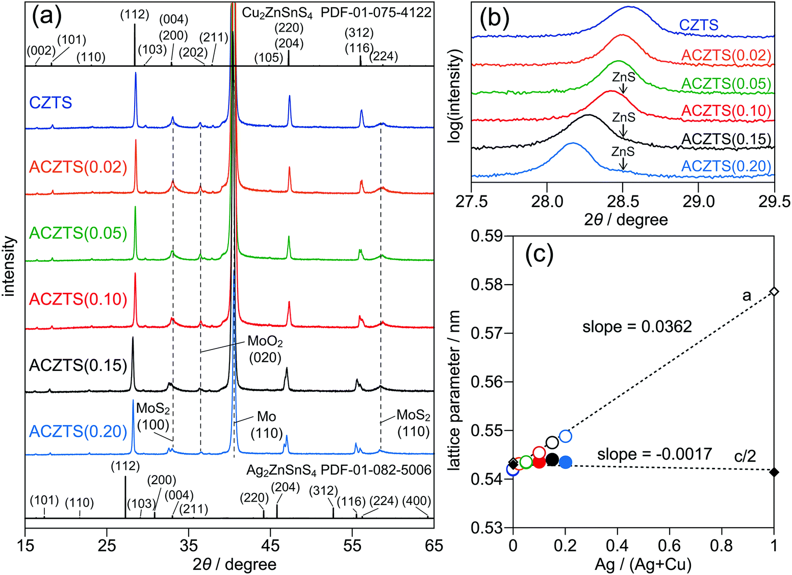 | ||
| Fig. 1 XRD patterns (a and b) of CZTS and Ag-incorporated thin films deposited on Mo/glass. (c) Lattice parameter variations obtained from these patterns (circles) and standard profiles of CZTS (PDF-01-075-4122) and Ag2ZnSnS4 (PDF-01-082-5006). | ||
As calculated from these reflections, the length of the a-axis of the kesterite unit cell increased linearly with an increase in the Ag content, whereas the length of the c-axis was almost constant regardless of the Ag content (Fig. 1c). Moreover, extrapolations of these lattice parameters to the Ag/(Ag + Cu) ratio of 1.0 showed good agreement with those of pure Cu-free kesterite Ag2ZnSnS4 calculated from a standard profile (PDF-01-082-5006). Thus, all of the Ag components in the Ag-incorporated films should exist mainly in their corresponding Cu sites of kesterite lattices.
Fig. 2 shows surface FE-SEM images of CZTS and Ag-incorporated films. Corresponding size distributions of grains, which were obtained by applying a normal distribution curve to the average minor diameter (Davr) and the standard deviation (SD) calculated from more than 50 grains for each sample, are also shown in this figure. The CZTS film shows densely packed well-grown grains of ca. 1 μm in size. Similar morphologies were also observed for the ACZTS(0.02) film. Further inclusion of Ag up to the Ag/(Ag + Cu) ratio of 0.10 (ACZTS(0.05) and ACZTS(0.10) films) induced obvious grain growth. Size distribution analyses suggest ca. 1.5-times increments of their grain sizes compared to those in the bare CZTS film. On the other hand, Ag-containing films including larger amounts of Ag (ACZTS(0.15) and ACZTS(0.20) films) showed appreciable reductions in their grain sizes by nearly one order of magnitude. Empirically, partial Ag replacement is known to be effective for grain growth in several chalcopyrite films50–52 as well as the present Ag-incorporated CZTS41 at least for an Ag/(Ag + Cu) ratio of less than 0.20 regardless of their fabrication processes. However, there is no report showing a detrimental effect of Ag incorporation on grain growth. Although detailed analyses should be performed, the observed suppression of grain growth is likely to be characteristic for the spray deposition method.
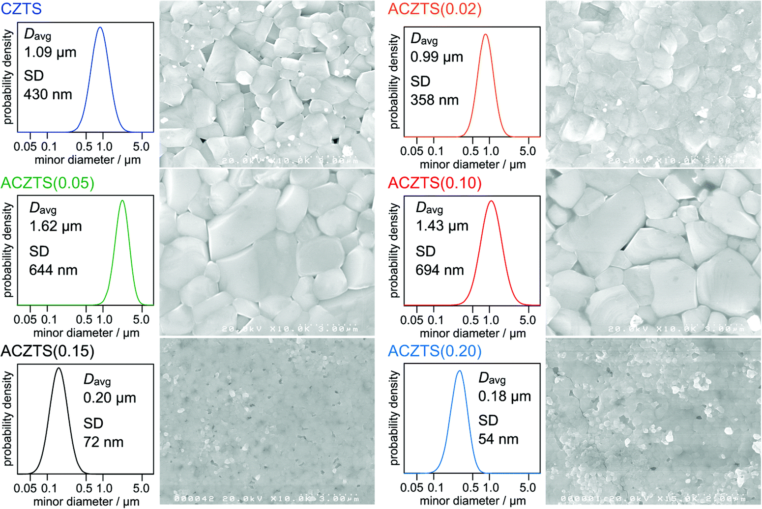 | ||
| Fig. 2 Surface FE-SEM images of CZTS and Ag-incorporated thin films deposited on Mo/glass. Size distributions of grains calculated from average minor diameters (Davgs) and standard deviations (SDs) obtained by measuring more than 50 grains are also shown on the left of each SEM image. | ||
It is known that surface modifications with both an n-type ultrathin layer (such as CdS and In2S3) and an HER catalyst (such as Pt metal nanoparticles) are indispensable for inducing efficient photocurrents.11,24,25 The present thin films also required these modifiers: regarding the n-type layer, specifically, the use of an In2S3–CdS double layer showed better HER ability than that of a simple CdS (or In2S3) single layer (Fig. S1, ESI†). As reported previously,32 the CdS layer should form the best p–n heterojunction for the CZTS-based photoabsorber; the main contribution of the In2S3 overlayer would be protection of direct contact of the CdS surface with the aqueous solution to avoid rapid oxidative degradation of CdS. Therefore, we used samples modified with the In2S3–CdS double layer and a Pt catalyst as photocathodes. Fig. 3a shows the current density-potential (J–V) curves obtained by linear sweep voltammetry (LSV) analyses of photocathodes based on CZTS and Ag-incorporated CZTS films under chopped sunlight (AM 1.5G) illumination. The photocathode based on the CZTS film showed a photocurrent density of 9 mA cm−2 at ERHE = 0 V. The maximum HC-STH (HC-STHmax) of the photocathode estimated from the J–V curve reached 1.6% (Fig. 3b); the photocurrent onset of the sample, defined as a potential (ERHE) showing 0.1% of HC-STH, was estimated to be 0.72 V. Although the photocathode based on an Ag-incorporated CZTS film with low Ag content (ACZTS(0.02)) showed almost the same J–V curve as that of the bare CZTS-based photocathode, obvious increases in PEC characteristics were observed for photocathodes based on the ACZTS(0.05) and ACZTS(0.10) films, whereas appreciable drops in PEC properties appeared for the photocathodes based on the ACZTS(0.15) and ACZTS(0.20) films. For a quantitative comparison of these PEC properties, typical PEC parameters, i.e., HC-STHmax and photocurrent onset, were extracted and they were plotted against the Ag/(Ag + Cu) ratio (Fig. 3c). There were appreciable improvements in HC-STHmax values, which reached more than 2% when photocathodes based on the ACZTS(0.05) and ACZTS(0.10) films were used, though the photocurrent onset was not affected by the Ag incorporation (see below) probably due to similarities of interface properties of p–n heterojunctions in these photocathodes. The highest HC-STHmax value of 2.4% was obtained by the ACZTS(0.10)-based photocathode sample. On the other hand, appreciable drops in PEC properties appeared for photocathodes based on ACZTS(0.15) and ACZTS(0.20) films. HC-STHmax values of these photocathodes were reduced to almost one-third of the HC-STHmax value of a bare CZTS-based photocathode.
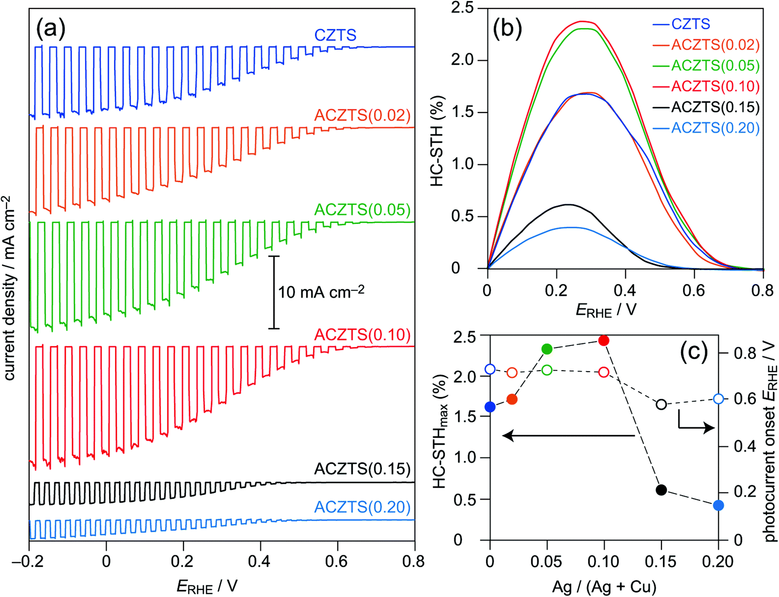 | ||
| Fig. 3 (a) Current density–potential (J–V) curves of CZTS and Ag-incorporated thin films modified with a chemical bath-deposited CdS layer and Pt deposits in an Na2HPO4/NaH2PO4 solution (pH 6.5) under chopped solar simulated AM 1.5G light irradiation. (b) Corresponding HC-STH plots extracted from these J–V curves for each sample. (c) Plots of HC-STHmax and photocurrent onset ERHEs of these photocathodes against Ag/(Ag + Cu) ratios of CZTS and Ag-incorporated thin films. | ||
To characterize the effect of Ag incorporation into the CZTS lattice of the film on photoexcited charge recombination occurring inside the film, PL and TRPL measurements were performed for CdS-covered CZTS and Ag-incorporated CZTS films. It is known that bare kesterite and chalcopyrite films are degraded by exposure to open air and the degradation has an impact on minority carrier lifetime.53–55 To examine the bulk properties of the films in this study, therefore, CdS-covered films, i.e., CZTS and Ag-incorporated films passivated by a CdS layer, were chosen for both PL and TRPL measurements. For PL emission properties, the normalized PL spectra of all samples showed similar results in terms of peak shape and peak position, as shown in Fig. 4a: as analysed by applying the conventional Gaussian equation, all of the measured samples showed peak-top positions of ca. 940 nm and peak widths of ca. 70 nm (Table 1). The PL peak position value corresponded to 1.32 eV in the energy scale; the value is much smaller than that of the band gap energy of CZTS (ca. 1.50 eV). In accordance with the previous PL study on selenosulfide Cu-based kesterites (Cu2ZnSn(Se,S)4), the observed PL emission is assignable to the band–impurity recombination.53 Photoabsorption properties of Ag-incorporated CZTS crystals examined by the powder system proved that band gap energies of Ag-incorporated CZTS crystals in the present Ag content (i.e., Ag/(Ag + Cu) ratio up to 0.2) are not significantly changed by the Ag incorporation.56,57 Moreover, band edge positions, i.e., the maximum energies of valence band (VBMs) and minimum energies of conduction band (CBMs), of the CZTS and ACZTS films were suggested to be comparable to at least the ACZTS with an Ag/(Ag + Cu) ratio up to 0.1.43 Therefore, the optical absorption properties of the present Ag-incorporated CZTS crystals are assumed to be almost the same as those of the Ag-free CZTS film. Based on these considerations, the observed PL emissions for the Ag-containing samples measured in the present study are also assignable to the same band–impurity recombination path. Thus, in the following discussion, we assumed that the Ag incorporation of the present sample did not induce critical changes in the defect structure(s)-affected radiative recombination.
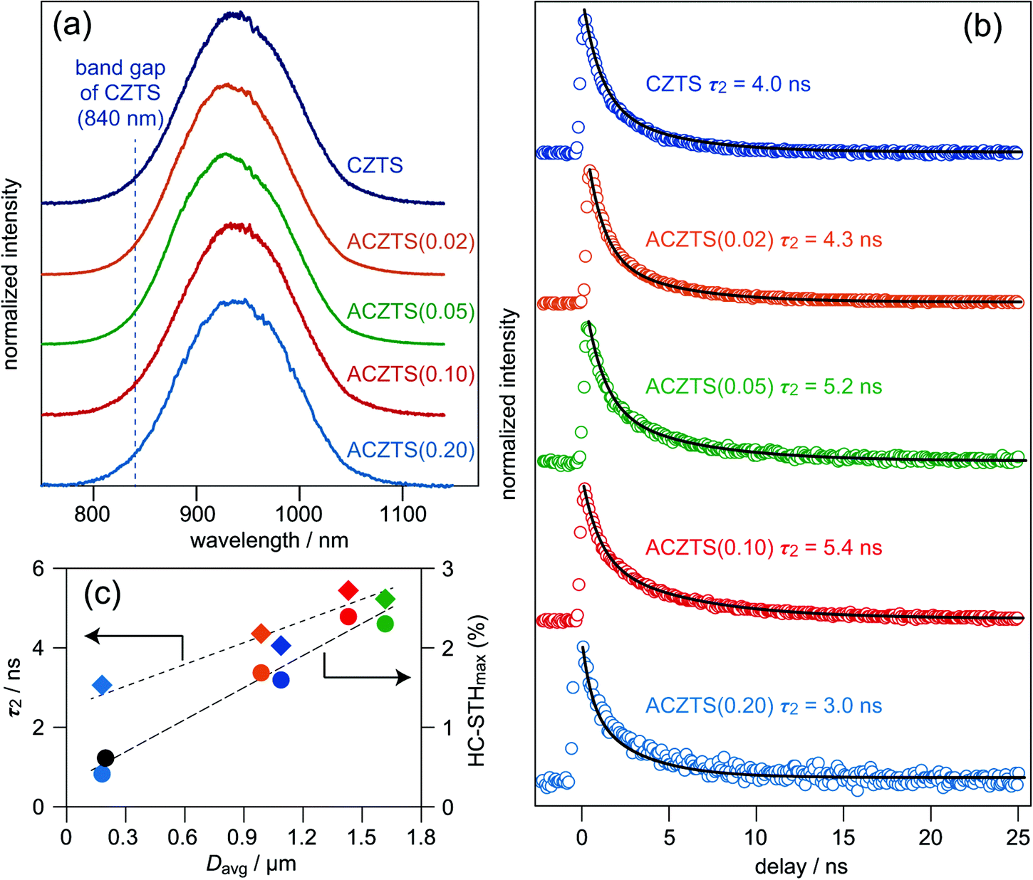 | ||
| Fig. 4 (a) Steady-state PL and (b) TRPL spectra of CZTS and Ag-incorporated thin films covered with a chemical bath-deposited CdS layer. (c) Dependence of τ2 and dependence of HC-STHmax obtained by TRPL measurement (for τ2) and J–V curves shown in Fig. 3 (for HC-STHmax) on the contents of Ag (Ag/(Ag + Cu)) in CZTS and Ag-incorporated thin films. | ||
| Sample | λ 0 /nm | w /nm | τ 1 /ns | τ 2 /ns | C 1/C2b |
|---|---|---|---|---|---|
| a Peak position (λ0) and width (w) determined by fitting each PL spectra with the conventional Gaussian equation: I(λ) = exp{−(λ − λ0)/w}2. b Parameters obtained by fitting TRPL decay curves with the double-exponential function given in the main text. | |||||
| CZTS | 941 | 72.2 | 1.00 | 4.01 | 1.75 |
| ACZTS(0.02) | 934 | 71.6 | 0.95 | 4.30 | 1.80 |
| ACZTS(0.05) | 934 | 74.3 | 1.04 | 5.18 | 1.53 |
| ACZTS(0.10) | 940 | 74.0 | 0.98 | 5.42 | 1.19 |
| ACZTS(0.20) | 940 | 76.2 | 0.56 | 2.96 | 0.91 |
As shown in Fig. 4b, the room temperature TRPL signal indicates a gradual increase in PL lifetime with an increase in the Ag content. The decay curves could be fitted by the following double-exponential function:
I(t) = C1![[thin space (1/6-em)]](https://www.rsc.org/images/entities/char_2009.gif) exp(−t/τ1) + C2exp(−t/τ2), exp(−t/τ1) + C2exp(−t/τ2), |
| 1/τPL = 1/τrad + 1/τnr. |
As shown in Fig. 4c, there is a clear trend for an increase in minority carrier lifetime with an increase in Davr. The HC-STHmax values are also increased with an increase in the grain size in the kesterite films. The integrated PL intensity of the corresponding samples also roughly follow a similar tendency (data not shown). These results suggest that a deep defect(s) that existed at grain boundaries in the kesterite films would be a probable center for inducing SRH recombination. Although the origin(s) of defect structure(s) at grain boundaries has not yet been clarified, suppression of the effective area of SRH recombination would be achieved by an increase in grain size, resulting in improvements of HC-STHmax. Apart from the effect of grain boundaries, acceptor densities (NAs) calculated from capacitance–voltage (C–V) analyses of photovoltaic devices indicated that there was no appreciable decrease in NA observed for the ACZTS film with a moderate Ag content (ACZTS(0.10)).43 As mentioned above, a theoretical study suggested that the formation energy of the CuZn antisite defect is much lower than other point defects such as VCu,47 whereas the formation energy of the AgZn antisite defect is relatively high since there are significant differences in the ionic radii between Ag and Zn ions.46 Assuming that the Ag incorporation reduces the number of CuZn antisite defects, comparable values of NAs between the ACZTS(0.10) film and the CZTS film suggest achievement of a successful combination of suppression of the formation of unfavourable CuZn and increment of favourable VCu in the kesterite lattice of the ACZTS(0.10) film. On the other hand, significant reductions in grain sizes observed for the photocathode based on Ag-incorporated CZTS films with a relatively large Ag content mainly appeared to have detrimental effects of an increase in the effective area of the grain boundaries, leading to a drop of their PEC performances.
As discussed in a previous report on the solar cell properties of Ag-incorporated films obtained by spray deposition, the best parameters were obtained by the cell based on ACZTS(0.02).43 Based on the fact that ACZTS films with relatively large grains (ACZTS(0.05) and ACZTS(0.10)) had many pinholes over the entire surface as observed at a relatively low magnification using a laser microscope,43 the inconsistency with the present PEC results as well as minority carrier lifetimes is likely to be due to the occurrence of shunts in the solar cell device induced by such pinholes, whereas the present PEC device is free from the unfavourable effect of pinholes, and thus there are many opportunities for further functionalization and/or survey of materials for PEC applications without paying much attention to pinhole formation in a newly developed semiconductor film. This would be a significant characteristic of the PEC device that is superior to a solar cell.
Fig. 5a shows a time course curve of H2 gas liberation over the photocathode based on a CZTS film at ERHE = 0 V under illumination from simulated sunlight (AM 1.5G). A current density profile during hydrogen production and the sum of half of the electrons passing through the outer circuit (e−/2) during H2 liberation at a certain interval are also plotted in this figure. The amount of H2 produced in the gas phase increased proportionally at a rate (per 1 cm2) of 157 μmol h−1 cm−2. The corresponding e−/2 plot (slope: 161 μmol h−1 cm−2) was consistent with the H2 liberation, i.e., the faradaic efficiency, defined as the ratio in percent of the rate of H2 evolution to that of e−/2 during 3 h photoirradiation, was estimated to be almost unity (ca. 98%). In addition, the observed constant photocurrent flow during the reaction indicated almost no degradation of the photocathode. As shown in Fig. 5b and c, a similar monotonous increase in H2 accumulation was also observed when the reaction was performed at applied potentials (ERHEs) of 0.25 V and 0.40 V. From the slopes of time course curves, the rates of H2 evolution (per 1 cm2) were calculated to be 36 μmol h−1 cm−2 at ERHE = 0.25 V and 3.8 μmol h−1 cm−2 at ERHE = 0.4 V. However, in these power generation potential regions, gradual drops in the rates of H2 liberation and photocurrent density profiles were also observed, suggesting the occurrence of degradation. Our recent studies have shown that significant improvements can be achieved by surface loadings of different n-type modifiers instead of the present In2S3/CdS, such as an HfO2/CdS double layer35 and an HfO2/CdS/HfO2 triple layer.36 Although the other factors affecting durability of the present photocathode, such as stability of the incorporated Ag component, should also be clarified, applications of Ag incorporation to those stabilized devices are now in progress.
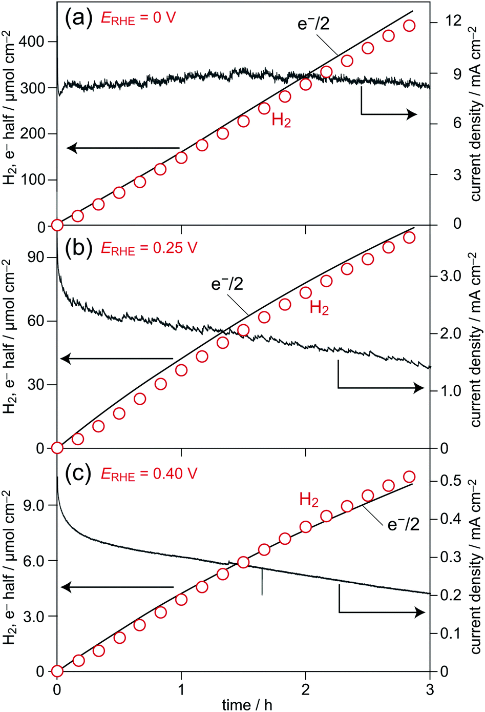 | ||
| Fig. 5 Time profiles of H2 evolution, half of the electrons passing through the outer circuit (e−/2), and photocurrent density over the photocathode composed of an ACZTS(0.10) film measured at different applied potentials (ERHEs). The active area of the used photocathode was 0.33 cm2. | ||
Conclusions
The effects of the incorporation of Ag into the crystalline lattice of a CZTS film on its morphological, PEC, and minority carrier dynamic properties were investigated. Obvious morphological changes were observed among the samples with different Ag contents. The photocathodes derived from the Ag-incorporated CZTS films having relatively large grains showed better PCE properties for H2 production than those of photocathodes based on bare CZTS and Ag-incorporated CZTS films having relatively small grains. Minority carrier lifetimes also followed these trends: relatively long lifetimes were obtained from samples that were highly active for PEC water reduction. Although the photocathodes did not have sufficient durability under operations in power-generating potential regions, the observed simple correlations among morphological, PEC, and carrier lifetime properties should be a useful guide for designing active photocathodes not only for H2 production but also for other photosynthetic reactions.Author contributions
S. Ikeda: conceptualization, methodology, supervision, project administration, writing – original draft, writing – review and editing; T. H. Nguyen: investigation, visualization; R. Okamoto: investigation; I. Abdellaoui: investigation, visualization; M. M. Islam: formal analysis, writing – review and editing; T. Harada: investigation, formal analysis; R. Abe: methodology; T. Sakurai: formal analysis, writing – review and editing.Conflicts of interest
There are no conflicts to declare.Acknowledgements
This work was supported by JSPS Grants-in-Aid for Scientific Research (KAKENHI), awards no. 19H02656, 19H02822, and 20H05120.Notes and references
- M. G. Walter, E. L. Warren, J. R. McKone, S. W. Boettcher, Q. Mi, E. A. Santori and N. S. Lewis, Chem. Rev., 2010, 110, 6446–6473 CrossRef CAS PubMed.
- I. Roger, M. A. Shipman and M. D. Symes, Nat. Rev. Chem., 2017, 1, 0003 CrossRef CAS.
- W. Yang and J. Moon, ChemSusChem, 2018, 11, 1–12 CrossRef.
- L. Zhang, Y. Li, X. Li, C. Li, R. Zhang, J.-J. Delaunay and H. Zhu, Nano Energy, 2016, 28, 135–142 CrossRef CAS.
- J. Kim, W. Yang, Y. Oh, H. Lee, S. Lee, H. Shin, J. Kim and J. Moon, J. Mater. Chem. A, 2017, 5, 2180–2187 RSC.
- J. J. Li, X. X. Han, M. Wang, Y. Zhao and C. Dong, New J. Chem., 2018, 42, 4114–4120 RSC.
- J. Tan, W. Yang, Y. Oh, H. Lee, J. Park, R. Boppella, J. Kim and J. Moon, Adv. Energy Mater., 2019, 9, 1900179 CrossRef.
- K. Wang, D. Huang, L. Li, K. Feng, T. Harada, S. Ikeda, J. Li and F. Jiang, Sol. RRL, 2020, 1900559 CrossRef CAS.
- T. Minegishi, A. Ohnishi, Y. Pihosh, K. Hatagami, T. Higashi, M. Katayama, K. Domen and M. Sugiyama, APL Mater., 2020, 8, 041101 CrossRef CAS.
- D. Huang, L. Li, K. Wang, Y. Li, K. Feng and F. Jiang, Nat. Commun., 2021, 12, 3795 CrossRef CAS PubMed.
- D. Yokoyama, T. Minegishi, K. Maeda, M. Katayama, J. Kubota, A. Yamada, M. Konagai and K. Domen, Electrochem. Commun., 2010, 12, 851–853 CrossRef CAS.
- M. Moriya, T. Minegishi, H. Kumagai, M. Katayama, J. Kubota and K. Domen, J. Am. Chem. Soc., 2013, 135, 3733–3735 CrossRef CAS PubMed.
- H. Kumagai, T. Minegishi, Y. Moriya, J. Kubota and K. Domen, J. Phys. Chem. C, 2014, 118, 16386–16392 CrossRef CAS.
- M. G. Mali, H. Yoon, B. N. Joshi, H. Park, S. S. Al-Deyab, D. C. Lim, S. Ahn, C. Nervi and S. S. Yoon, ACS Appl. Mater. Interfaces, 2015, 7, 21619–21625 CrossRef CAS PubMed.
- H. Kaneko, T. Minegishi, M. Nakabayashi, N. Shibata and K. Domen, Angew. Chem., Int. Ed., 2016, 55, 15329–15333 CrossRef CAS PubMed.
- N. Guijarro, M. S. Prévot, X. Yu, X. A. Jeanbourquin, P. Bornoz, W. Bourée, M. Johnson, F. Le Formal and K. Sivula, Adv. Energy Mater., 2016, 6, 1501949 CrossRef.
- M. Li, R. Zhao, Y. Su, J. Hu, Z. Yang and Y. Zhang, Appl. Catal., B, 2017, 203, 715–724 CrossRef CAS.
- A. D. DeAngelis, K. Horsley and N. Gaillard, J. Phys. Chem. C, 2018, 122, 14304–14312 CrossRef CAS.
- H. Kobayashi, N. Sato, M. Orita, Y. Kuang, H. Kaneko, T. Minegishi, T. Yamada and K. Domen, Energy Environ. Sci., 2018, 11, 3003–3009 RSC.
- M. Chen, Y. Liu, C. Li, A. Li, X. Chang, W. Liu, Y. Sun, T. Wang and J. Gong, Energy Environ. Sci., 2018, 11, 2025–2034 RSC.
- B. Kim, G. S. Park, Y. J. Hwang, D. H. Won, W. Kim, D. K. Lee and B. K. Min, ACS Energy Lett., 2019, 4, 2937–2944 CrossRef CAS.
- S. Ikeda, W. Fujita, R. Okamoto, Y. Nose, R. Katsube, K. Yoshino and T. Harada, RSC Adv., 2020, 10, 40310–40315 RSC.
- S. Ikeda, R. Okamoto and S. Ishizuka, Appl. Phys. Lett., 2021, 119, 083902 CrossRef CAS.
- S. Ikeda, T. Nakamura, S. M. Lee, T. Yagi, T. Harada, T. Minegishi and M. Matsumura, ChemSusChem, 2011, 4, 262–268 CAS.
- Gunawan, W. Septina, S. Ikeda, T. Harada, T. Minegishi, K. Domen and M. Matsumura, Chem. Commun., 2014, 50, 8941–8943 RSC.
- J. Zhao, T. Minegishi, L. Zhang, M. Zhong, Gunawan, M. Nakabayashi, G. Ma, T. Hisatomi, M. Katayama, S. Ikeda, N. Shibata, T. Yamada and K. Domen, Angew. Chem., Int. Ed., 2014, 53, 11808–11812 CrossRef CAS PubMed.
- W. Septina, Gunawan, S. Ikeda, T. Harada, T. Higashi, R. Abe and M. Matsumura, J. Phys. Chem. C, 2015, 119, 8576–8583 CrossRef CAS.
- Gunawan, W. Septina, T. Harada, Y. Nose and S. Ikeda, ACS Appl. Mater. Interfaces, 2015, 7, 16086–16092 CrossRef CAS PubMed.
- D. Yokoyama, T. Minegishi, K. Jimbo, T. Hisatomi, G. Ma, M. Katayama, J. Kubota, H. Katagiri and K. Domen, Appl. Phys. Express, 2010, 3, 101202 CrossRef.
- G. Ma, T. Minegishi, D. Yokoyama, J. Kubota and K. Domen, Chem. Phys. Lett., 2011, 501, 619–622 CrossRef CAS.
- P. Dai, G. Zhang, Y. Chen, H. Jiang, Z. Feng, A. Lin and J. Zhan, Chem. Commun., 2012, 48, 3006–3008 RSC.
- F. Jiang, Gunawan, T. Harada, Y. Kuang, T. Minegishi, K. Domen and S. Ikeda, J. Am. Chem. Soc., 2015, 137, 13691–13697 CrossRef CAS PubMed.
- L. Rovelli, S. D. Tilley and K. Sivula, ACS Appl. Mater. Interfaces, 2013, 5, 8018 CrossRef CAS PubMed; W. Yang, Y. Oh, J. Kim, M. J. Jeong, J. H. Park and J. Moon, ACS Energy Lett., 2016, 1, 1127–1136 CrossRef.
- M. P. Suryawanshi, U. V. Ghorpade, S. W. Shin, M. G. Gang, X. Wang, H. Park, S. H. Kang and J. H. Kim, ACS Catal., 2017, 7, 8077–8089 CrossRef CAS.
- D. Huang, K. Wang, L. Yu, T. H. Nguyen, S. Ikeda and F. Jiang, ACS Energy Lett., 2018, 3, 1875–1881 CrossRef CAS.
- D. Huang, K. Wang, L. Li, K. Feng, N. An, S. Ikeda, Y. Kuang, Y. H. Ng and F. Jiang, Energy Environ. Sci., 2021, 14, 1480–1489 RSC.
- Y. F. Tay, H. Kaneko, S. Y. Chiam, S. Lie, Q. Zheng, B. Wu, S. S. Hadke, Z. Su, P. S. Bassi, D. Bishop, T. C. Sum, T. Minegishi, J. Barber, K. Domen and L. H. Wong, Joule, 2018, 2, 537–548 CrossRef CAS.
- X. Wen, W. Luo, Z. Guan, W. Huang and Z. Zou, Nano Energy, 2017, 41, 18–26 CrossRef CAS.
- S. Ikeda, S. Fujikawa, T. Harada, T. H. Nguyen, S. Nakanishi, T. Takayama, A. Iwase and A. Kudo, ACS Appl. Energy Mater., 2019, 2, 6911–6918 CrossRef CAS.
- Y. Zhou, D. Shin, E. Ngaboyamahina, G. Han, C. B. Parker, D. B. Mitzi and J. T. Glass, ACS Energy Lett., 2018, 3, 177–183 CrossRef CAS.
- Z. Xu, Z. Guan, J. Yang and G. Li, ACS Appl. Energy Mater., 2019, 2, 2779–2785 CrossRef CAS.
- Y. F. Tay, S. S. Hadke, M. Zhang, N. Lim, S. Y. Chiamd and L. H. Wong, J. Mater. Chem. A, 2020, 8, 8862–8867 RSC.
- T. H. Nguyen, T. Kawaguchi, J. Chantana, T. Minemoto, T. Harada, S. Nakanishi and S. Ikeda, ACS Appl. Mater. Interfaces, 2018, 10, 5455–5463 CrossRef CAS PubMed.
- W.-C. Huang, S.-Y. Wei, C.-H. Cai, W.-H. Ho and C.-H. Lai, J. Mater. Chem. A, 2018, 6, 15170–15181 RSC.
- Y. Qi, Q. Tian, Y. Meng, D. Kou, Z. Zhou, W. Zhou and S. Wu, ACS Appl. Mater. Interfaces, 2017, 9, 21243–21250 CrossRef CAS PubMed.
- Z. K. Yuan, S. Chen, H. Xiang, X. G. Gong, A. Walsh, J. S. Park, I. Repins and S. H. Wei, Adv. Funct. Mater., 2015, 25, 6733–6743 CrossRef CAS.
- S. Chen, A. Walsh, X. G. Gong and S. H. Wei, Adv. Mater., 2013, 25, 1522–1539 CrossRef CAS PubMed.
- S. Bourdais, C. Choné, B. Delatouche, A. Jacob, G. Larramona, C. Moisan, A. Lafond, F. Donatini, G. Rey, S. Siebentritt, A. Walsh and G. Dennler, Adv. Energy Mater., 2016, 6, 1502276 CrossRef.
- Y.-F. Qi, D.-X. Kou, W.-H. Zhou, Z.-J. Zhou, Q.-W. Tian, Y.-N. Meng, X.-S. Liu, Z.-L. Du and S. X. Wu, Energy Environ. Sci., 2017, 10, 2401–2410 RSC.
- L. Zhang, T. Minegishi, J. Kubota and K. Domen, Phys. Chem. Chem. Phys., 2014, 16, 6167–6174 RSC.
- L. Zhang, T. Minegishi, M. Nakabayashi, Y. Suzuki, K. Seki, K. N. Shibata, J. Kubota and K. Domen, Chem. Sci., 2015, 6, 894–901 RSC.
- W. Septina, M. Sugimoto, D. Chao, Q. Shen, S. Nakatsuka, Y. Nose, T. Harada and S. Ikeda, Phys. Chem. Chem. Phys., 2017, 19, 12502–12508 RSC.
- M. A. Halim, M. M. Islam, X. Luo, T. Sakurai, N. Sakai, T. Kato, H. Sugimoto, H. Tampo, H. Shibata, S. Niki and K. Akimoto, Jpn. J. Appl. Phys., 2015, 54, 08KC15 CrossRef.
- M. Buffiere, G. Brammertz, A.-A. El Mel, N. Lenaers, Y. Ren, A. E. Zaghi, Y. Mols, C. Koeble, J. Vleugels, M. Meuris and J. Poortmans, Proc. IEEE 39th Photovoltaic Specialists Conf. (PVSC), 2013, p. 1941.
- H. Tangara, S. Zahedi-Azad, J. Not, J. Schick, A. Lafuente-Sampietro, M. M. Islam, R. Scheer and T. Sakurai, J. Appl. Phys., 2021, 129, 183108 CrossRef CAS.
- S. Ikeda, T. Nakamura, T. Harada and M. Matsumura, Phys. Chem. Chem. Phys., 2010, 12, 13943–13949 RSC.
- W. Gong, T. Tabata, K. Takei, M. Morihama, T. Maeda and T. Wada, Phys. Status Solidi C, 2015, 12, 700–703 CrossRef CAS.
- G. Brammertz, M. Buffière, Y. Mevel, Y. Ren, A. E. Zaghi, N. Lenaers, Y. Mols, C. Koeble, J. Vleugels, M. Meuris and J. Poortmans, Appl. Phys. Lett., 2013, 102, 013902 CrossRef.
- F. Jiang, S. Ikeda, Z. Tang, T. Minemoto, W. Septina, T. Harada and M. Matsumura, Prog. Photovoltaics, 2015, 23, 1884–1895 CAS.
Footnote |
| † Electronic supplementary information (ESI) available: LSV plot of CZTS-based photocathodes with several surface modifications. See DOI: 10.1039/d1cp04075h |
| This journal is © the Owner Societies 2022 |