
Silicon and indium as secondary cathodes for the analysis of solid alumina and sapphire by slow-flow direct-current glow discharge mass spectrometry
Jochen
Busam
 *,
Gagan
Paudel
and
Marisa
Di Sabatino
*,
Gagan
Paudel
and
Marisa
Di Sabatino
Department of Materials Science and Engineering, Norwegian University of Science and Technology (NTNU), 7491 Trondheim, Norway. E-mail: jochen.busam@ntnu.no
First published on 30th November 2021
Abstract
We demonstrate and compare the capabilities of indium and silicon as secondary cathodes for the analysis of flat, solid alumina and sapphire matrices by direct current glow discharge mass spectrometry (dc-GDMS). The mask designs and the glow discharge conditions are optimised for signal ratio and absolute intensity. The mask material was found to be a small factor in matrix to mask ratio and signal intensity despite the large difference in properties between indium and silicon. The results indicate that the discharge conditions play the most significant role. The mask material did not appear to affect the RSFs. On sapphire with indium, the possible discharge conditions and performance were limited due to a collapse of discharge. This was not the case for silicon, which proves to be a good alternative as secondary cathode material.
A Introduction
Direct current glow discharge mass spectrometry (dc-GDMS) on flat, solid, non-conducting samples is realised through the secondary cathode technique.1 Here, a conducting mask is placed on the sample and attracts plasma ions that sputter the mask atoms, which redeposit on the sample. This causes the non-conducting sample to also attract ions and be sputtered. The most reported mask design in the literature is that of a single round opening in a tantalum secondary cathode.1–6 Notably, with a pin-shaped tantalum holder, Nu Instruments demonstrated the analysis of alumina powder and sapphire wafers.7There are two main criteria for a good mask material: (i) it should be as pure as possible to prevent any signal contributions from impurities in the mask; (ii) it should have a low sputtering yield, as this seems beneficial to a stable discharge and sample matrix to mask signal ratios with a small mask contribution.2 The fulfilment of both criteria should enable low detection limits with the secondary cathode method in the GDMS. Tantalum has a low sputtering yield8–10 and is available in high purities. More recently, several slit openings have been reported for an indium mask, which is available in higher purities than tantalum.11,12 A possible drawback of indium is its high sputtering yield.10
The logical step to further improve the secondary cathode method is to choose a mask material that has lower sputtering yield and higher purity than tantalum and indium. An element that would combine ultra-high purity with a low sputtering yield is silicon.8–10 The purity of silicon can be on the ppq level even for common elements like iron.13 Silicon could allow for major improvements to the secondary cathode technique regarding detection limits. Silicon is a standard product in the semi-conductor industry and, therefore, readily available at a low cost. In the form of wafers, it can be purchased cleanly polished and at the required thicknesses to be used as secondary cathode.14 Also, silicon wafers have been previously used as auxiliary component in the context of dc-GDMS.15
In order to evaluate the performance of silicon as mask material, we compare both silicon and indium masks on Al2O3 samples. High-purity Al2O3 has, in its different forms, applications in various types of industries. As alumina ceramic, it is e.g. used for crucibles in the metal and glass industry. As single crystal, called sapphire, it is used as substrate in the semi-conductor industry. The chemical analysis of Al2O3 on the trace impurity level proves to be difficult, as the material is extremely resistant to chemical digestion. Also, its hardness makes crushing difficult and prone to contamination. dc-GDMS is a prime candidate to directly analyse such refractory materials, as it does not require digestion or crushing steps. Additionally, its high 1D resolution allows μm accurate depth profiling of flat samples.16,17
Quantification and RSF
In dc-GDMS, the effects of different sample matrices and discharge conditions on quantification are regarded as small.18 These external effects, and element intrinsic effects are incorporated into the analysis by so-called relative sensitivity factors (RSFs),19,20 as shown in eqn (1). CX/M is the concentration of element X contained in a sample matrix M, while Ix and IM represent the measured, abundance corrected ion beam intensity for the element and the matrix, respectively.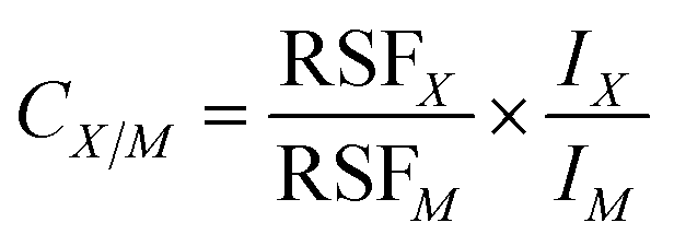 | (1) |
B Experimental
Instrumentation
This work was performed with a double focusing low-flow dc-GDMS, the Nu Instruments Astrum. The instrument was operated in constant current mode with a mass resolution of 4000. The standard RSFs provided with the instrument and used in these experiments are based on the work by Vieth and Huneke.19 The experiments were conducted with a flat-sample holder tantalum anode plate opening of 10 mm.Samples
Two types of samples with the chemical structure Al2O3 were investigated. One was the alumina ceramics used as insulator in the flat holders of the Astrum GDMS. These ceramics are commonly polycrystalline on the μm scale with glassy intermediate phases.21 The other sample was a sapphire single crystal. Both samples were polished down in several steps to 1 μm diamond grit and rinsed with ethanol and DI water. The sapphire proved to be too hard to obtain a smooth surface, as it still showed scratches of several μm depth.Masks
The indium masks were prepared from 7N indium shots provided by RASA Industries. The shots were pressed flat to a thickness of 0.2 mm. The mask openings were cut out with a ZrO2 blade of fixed size to provide reproducible dimensions and prevent contamination by metallic impurities. As the ZrO2 blades are inert and hard, no zirconium contamination is expected from them. The indium masks were etched for 1 min in 65% HNO3 to remove oxide layers and possible surface contamination. Finally, the masks were rinsed with DI water and ethanol and air dried.The silicon masks were prepared from as-received, chemically polished float zone (FZ) silicon wafers. The wafer thickness was 0.25 mm. The wafers were boron doped with concentrations of approximately 100 ppbw, yielding a resistivity of 1.2 Ω cm. The wafers were laser cut with a Rofin PowerLine F-30 at 1064 nm wavelength and 30 W power. During the cutting the wafers were placed on another wafer to avoid the laser penetrating into the underlying metal which could cause contamination. No further etching or polishing was applied after the cutting.
Mask design
For the indium mask, round openings of 6 and 8 mm were compared to the previously established design with three slits12 in terms of matrix to mask signal ratio and signal intensity. For the silicon mask, different aperture designs and dimensions were investigated. Round openings of 4–8 mm and designs with 3–5 slits of varying dimensions.Limit of detection
The limit of detection (LOD) is defined by three times the standard deviation of the background, as suggested by Milton and Hutton.2 The background thereby is the sum of instrument noise and signal contribution from the contaminants in the masks.Methodology
Measurements were acquired five or six times at 80 ms with the Faraday cup and at 320 ms with the ion counter for elements of low concentration.For Al2O3, the measured values were corrected for the contribution of impurities contained in the mask based on the Al27 signal intensity and the measured blank mask concentrations. As only Al27 and not O16 is measured, a stoichiometric correction of 0.53 is applied.
For the selection of discharge conditions two criteria were considered: (i) stable readback values of current and voltage and hence stable signal; (ii) highest absolute intensity of matrix signal as well as matrix to mask signal ratios with a small mask contribution. Discharge condition selection/optimization can also be done using other selection criteria, for instance minimum variation in RSFs.22 The criteria presented in this work are suitable for analysis of non-conducting samples, as demonstrated in earlier publications.14
C Results
Impurity concentration in the masks
For both indium and silicon, the masks showed similar impurity concentrations as the basic material. An example of the measured impurities in the masks is shown in Table 1. For silicon, all elements were below the detection limit, thus only an upper limit is given. The FZ silicon produced a comparably low ion beam intensity, which is the reason for the high detection limits compared to indium. It is possible that the silicon values are far below the upper limits given here.| Element | In mask | RSD% | Si mask | RSD% |
|---|---|---|---|---|
| Ti | 0.59 | 13 | ≤1.1 | 26 |
| V | 0.024 | 35 | ≤0.78 | 20 |
| Cr | 0.34 | 14 | ≤0.53 | 27 |
| Zr | ≤0.18 | 19 | ≤1.6 | 26 |
| Nb | 0.17 | 14 | ≤2.1 | 21 |
| Mo | 0.46 | 21 | ≤1.4 | 29 |
| W | 0.24 | 13 | ≤1.1 | 25 |
Mask design
For the indium mask, the design with three slits, shown in Fig. 1a, performed better in terms of matrix to mask ratio and intensity than any design with a round opening. The best round design was found in an opening of 6 mm and produced a matrix to mask ratio of 1![[thin space (1/6-em)]](https://www.rsc.org/images/entities/char_2009.gif) :37 with an Al27 intensity of 9.4 × 10⁸. The design with three slits produced a matrix to mask ratio of 1:4.3 with an Al27 intensity of 7.4 × 10⁹.
:37 with an Al27 intensity of 9.4 × 10⁸. The design with three slits produced a matrix to mask ratio of 1:4.3 with an Al27 intensity of 7.4 × 10⁹.
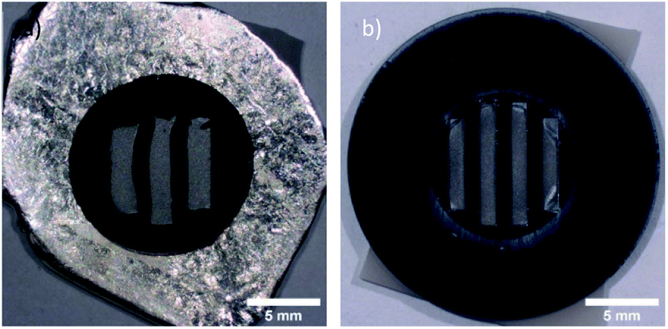 | ||
| Fig. 1 (a) indium mask with three slits on alumina after use, and (b) silicon mask with four slits on alumina after use. | ||
For silicon as well, the mask geometry with several rectangular slits performed better than the masks with a round opening. The best round design was found in an opening of 8 mm and produced a matrix to mask ratio of 1:34 with an Al27 intensity of 1.5 × 10⁸. The best design with slits produced a matrix to mask ratio of 1:5.8 with an Al27 intensity of 4.3 × 10⁹.
The optimum geometry was found with 4 slits of 1 mm width and 8 mm (central slits) and 6 mm length (peripheral slits), shown in Fig. 1b. A design with wider slits performed worse, possibly because of a shielding effect from charge build up due to the larger distance to a conductor. A design with 5 slits of 0.8 mm width and length from 6 to 9 mm performed similarly but was omitted due to the danger of the thin silicon parts breaking.
For both masks, no deposition of mask material was visible centrally inside the slits under the light microscope.
Discharge conditions
The exposed sample area is for both masks with slit design approximately 0.25 cm2.
Despite the large difference in sputtering yield, atomic weight and conductivity, the results regarding ratio and intensity for indium and silicon are rather similar under similar settings. The mask material itself thus seems to be a minor factor on matrix to mask ratio and intensity compared to the discharge settings.
:200 with an Al27 intensity of 6.3 × 10⁸. A clear cause for the collapse could not be determined.
For sapphire with a silicon mask, no collapse was observed. Thus, the optimal discharge settings could be established at 1.5 mA and 1950 V with an argon flow of around 0.21 sccm. This resulted in a matrix to mask ratio of 1:10 with an Al27 intensity of 2.9 × 10⁹. In this case, the silicon mask performs far better than the indium mask due to the different discharge settings.
For the silicon mask with very similar discharge conditions, sapphire yields a lower intensity and worse ratio than alumina despite the similar chemical structure. This points to an influence of the microstructure on the sputtering yield, as the single crystal appears more resistant.
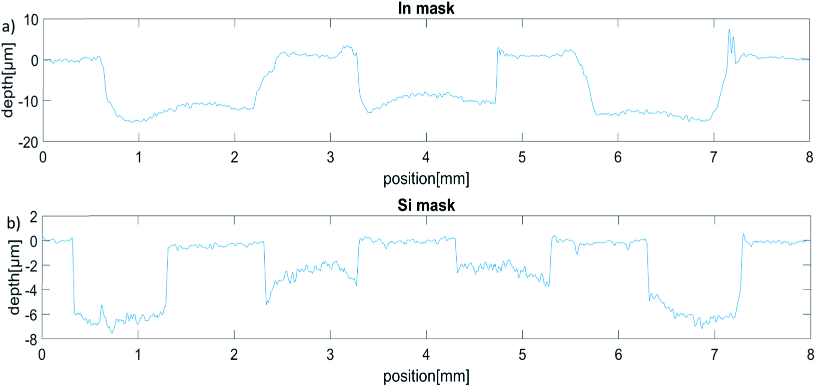 | ||
| Fig. 2 (a) crater profile with an indium mask on alumina after about 2 hours, and (b) crater profile with a silicon mask on alumina after about 1 hour. Notice the different depth scales, as the samples' runtimes deviated. | ||
For Si, the central slits are convex while the outer slits show a concave form and deeper penetration. This is reasonable again regarding the high voltage settings, as the outer slits lie close to the edge of the sample holder opening.
Both mask materials show a depth difference of approximately 5 μm between high and low point of the crater and approximately the same penetration speed.
Measured concentrations
| Element | Average | RSD% | Blank% |
|---|---|---|---|
| Ti | 9390 | 2.3 | 0.056 |
| V | 429 | 4.6 | 0.050 |
| Cr | 638 | 6.2 | 0.48 |
| Zr | 1390 | 4.0 | 0.12 |
| Nb | 84.0 | 15 | 1.5 |
| Mo | 76.9 | 16 | 5.2 |
| W | 140 | 10 | 1.5 |
| Element | Average | RSD% | Blank% |
|---|---|---|---|
| Ti | 9540 | 4.5 | 0.052 |
| V | 428 | 5.9 | 0.82 |
| Cr | 538 | 18 | 0.44 |
| Zr | 1220 | 9.9 | 0.57 |
| Nb | 5.74 | 55 | 62 |
| Mo | 68.5 | 31 | 8.4 |
| W | 122 | 19 | 3.9 |
Overall, the mask material shows no significant influence on the measured concentrations, and thus RSFs, under the same conditions. This is supported by the titanium and zirconium values, which are in the same periodic group and show no deviation to higher or lower values in one material.
The only element that did not suffer from contamination and had a reference value provided by the manufacturer was vanadium. The results for the indium and silicon masks are shown in Table 4. The reference value was given as 0.10 ppma. The measured values show a very good agreement between the indium and silicon masks, as was the case for alumina. The difference in discharge conditions do not appear to influence the measured concentration. Also, the measured values are well within the range of the reference value considering possible deviations in either measurement due to e.g., systematic errors.
| Mask | V | RSD% | Blank% |
|---|---|---|---|
| In | 42.3 | 20 | 24 |
| Si | 47.3 | 7.1 | 16 |
Table 5 shows the LODs for alumina. Both indium and silicon produce LODs at least in the single digit ppb range.
| Element | Indium mask | Silicon mask |
|---|---|---|
| Ti | 1.8 | ≤3.7 |
| V | 0.40 | ≤2.1 |
| Cr | 1.1 | ≤2.0 |
| Zr | ≤0.81 | ≤5.4 |
| Nb | 0.57 | ≤5.9 |
| Mo | 2.3 | ≤5.3 |
| W | 0.74 | ≤3.7 |
Table 6 shows LODs in sapphire. In this case, silicon performs significantly better than indium, due to running on optimal discharge conditions. And again, the silicon values are an upper limit. The sapphire LODs obtained here with the indium mask are comparable to the ones reported by Nu Instruments obtained with a pin-shaped tantalum holder.7 The LODs obtained here with the silicon mask are at least a factor 5–10 lower.
| Element | Indium mask | Silicon mask |
|---|---|---|
| Ti | 79 | ≤6.7 |
| V | 17 | ≤3.8 |
| Cr | 49 | ≤3.4 |
| Zr | ≤36 | ≤9.6 |
| Nb | 25 | ≤11 |
| Mo | 100 | ≤9.4 |
| W | 31 | ≤6.6 |
D Conclusion
For both indium and silicon as mask material, the design with several slits performed better than any design with a round opening in terms of signal intensity and matrix to mask signal ratio.Both indium and silicon appear well suited as mask material for the dc-GDMS analysis of alumina. Under similar discharge conditions their performance is comparable, and the measured values are in good agreement despite the large difference in properties (such as sputtering yield and conductivity) of the two mask materials. There appears to be no influence on the RSFs by the mask material and the dominant factor to the performance of the method is the discharge conditions.
For sapphire, a collapse of discharge was observed with the indium mask, limiting the possible discharge conditions. With the silicon mask, no collapse was observed, and the measurement could be taken under optimal discharge conditions. Despite a difference in discharge conditions between the two masks, the measured vanadium values were in good agreement and comparable to the reference value, indicating no significant RSF sensitivity for this element.
The behaviour of alumina and sapphire under glow discharge and consequently discharge stability is different. This is likely due to a difference in mechanical and electric properties. The crystal structure of sapphire appears to be more resistant to sputtering than the amorphous structure of alumina and it causes a collapse of discharge already at lower voltages.
Silicon has proven to be a valid alternative as mask material, though more efforts to quantify the concentrations in silicon are needed for a better correction. FZ silicon masks, laser cut from wafers, are highly reproducible and not prone to contamination, contrary to the soft indium that requires an etching step in preparation. In general, different mask materials are valuable for the secondary cathode method as one mask element itself or contaminants therein might be of interest for the measurement, or it might create interferences.
Conflicts of interest
There are no conflicts to declare.Acknowledgements
This work was carried out in the project “Crucibles for next generation high quality silicon solar cells (CruGenSi)”, project no. 268027, funded by the Research Council of Norway and industry partners.References
- S. L. Tong and W. W. Harrison, Glow discharge mass spectrometric analysis of non-conducting materials, Spectrochim. Acta, Part B, 1993, 48(10), 1237–1245, DOI:10.1016/0584-8547(93)80108-7.
- D. M. P. Milton and R. C. Hutton, Investigations into the suitability of using a secondary cathode to analyse glass using glow discharge mass spectrometry, Spectrochim. Acta, Part B, 1993, 48(1), 39–52, DOI:10.1016/0584-8547(93)80006-G.
- W. Schelles, S. De gendt, K. Maes and R. Van grieken, The use of a secondary cathode to analyse solid non-conducting samples with direct current glow discharge mass spectrometry: potential and restrictions, Fresenius. J. Anal. Chem., 1996, 355(7–8), 858–860, DOI:10.1007/s0021663550858.
- M. Betti, Use of a direct current glow discharge mass spectrometer for the chemical characterization of samples of nuclear concern, J. Anal. At. Spectrom., 1996, 11(9), 855–860, 10.1039/ja9961100855.
- S. De Gendt, W. Schelles, R. Van Grieken and V. Müller, Quantitative analysis of iron-rich and other oxide-based samples by means of glow discharge mass spectrometry, J. Anal. At. Spectrom., 1995, 10(9), 681–687, 10.1039/JA9951000681.
- A. Bogaerts, W. Schelles and R. Van Grieken, Analysis of Nonconducting Materials by DC Glow Discharge Spectrometry, Glow Discharge Plasmas in Analytical Spectroscopy, John Wiley & Sons, Ltd, 2003, pp. 293–315 Search PubMed.
- D. Barnhart, K. Putyera and G. Churchill, CHEMICAL PURITY DETERMINATIONS OF ADVANCED ALUMINA SAMPLES BY NU ASTRUM GLOW-DISCHARGE MASS SPECTROMETRY, Nu Astrum Glow-Discharge Mass Spectrometry, Nu Instruments Application Note AN15 Search PubMed.
- N. Laegreid and G. K. Wehner, Sputtering yields of metals for Ar+ and Ne+ ions with energies from 50 to 600 ev, J. Appl. Phys., 1961, 32(3), 365–369, DOI:10.1063/1.1736012.
- H. Oechsner, Sputtering-a review of some recent experimental and theoretical aspects, Appl. Phys., 1975, 8(3), 185–198, DOI:10.1007/BF00896610.
- M. P. Seah, Pure element sputtering yields using 500-1000 eV argon ions, Thin Solid Films, 1981, 81(3), 279–287, DOI:10.1016/0040-6090(81)90490-9.
- D. Barnhart, G. Churchill and A. Burrows, An Exploration of Sample Preparations and Detection Limits for Conductive, Semi-Conductive and Non-Conductive Materials as Pertaining to the Astrum HR-GDMS, in 2nd International Glow Discharge Spectroscopy Symposium, 2014 Search PubMed.
- J. Busam, G. Stokkan, A. M. F. Muggerud and M. Di Sabatino, Application of 7N In as secondary cathode for the dc-GDMS analysis of solid, fused high-purity quartz, J. Mass Spectrom., 2021, e4771, DOI:10.1002/jms.4771.
- E. B. McDonald, R. J. Smith, A. R. Hurley and D. L. Norman, Sub-parts-per-quadrillion sensitivity to contaminants in ultra-pure silicon via low-background instrumental neutron activation analysis, in Proceedings of the Fourth International Symposium on High Purity Silicon, 1996, pp. 554–563 Search PubMed.
- W. Schelles, S. De Gendt and R. E. van Grieken, Optimization of secondary cathode thickness for direct current glow discharge mass spectrometric analysis of glass, J. Anal. At. Spectrom., 1996, 11(10), 937–941 RSC.
- C. Modanese, L. Arnberg and M. Di Sabatino, Methodology to analyse small silicon samples by glow discharge mass spectrometry using a thin wafer mask, MethodsX, 2015, 2, e409–e414, DOI:10.1016/j.mex.2015.10.005.
- A. Raith, R. C. Hutton and J. C. Huneke, Optimization of quantitative depth profiling with glow discharge mass spectrometry. Part 1. Optimization studies on crater shape and time-depth conversion, J. Anal. At. Spectrom., 1993, 8(6), 867–873, 10.1039/JA9930800867.
- M. Di Sabatino, C. Modanese and L. Arnberg, Depth profile analysis of solar cell silicon by GD-MS, J. Anal. At. Spectrom., 2014, 29(11), 2072–2077, 10.1039/C4JA00175C.
- V. Hoffmann, M. Kasik, P. K. Robinson and C. Venzago, Glow discharge mass spectrometry, Anal. Bioanal. Chem., 2005, 381(1), 173–188 CrossRef CAS PubMed.
- W. Vieth and J. C. Huneke, Relative sensitivity factors in glow discharge mass spectrometry, Spectrochim. Acta, Part B, 1991, 46(2), 137–153, DOI:10.1016/0584-8547(91)80017-W.
- A. Bogaerts and R. Gijbels, Relative sensitivity factors in glow discharge mass spectrometry: the role of charge transfer ionization, J. Anal. At. Spectrom., 1996, 11(9), 841–847, 10.1039/ja9961100841.
- C. A. Powell-dogan and A. H. Heuer, Microstructure of 96% Alumina Ceramics: I, Characterization of the As-Sintered Materials, J. Am. Ceram. Soc., 1990, 73(12), 3670–3676 CrossRef CAS.
- G. Paudel and M. Di Sabatino, Quantification of discharge gas to optimize discharge parameters for relative sensitivity factors (RSFs) determination by slow-flow glow discharge mass spectrometry (GDMS), J. Anal. At. Spectrom., 2020, 35(11), 2748–2757, 10.1039/d0ja00281j.
- J. Rumble, CRC Handbook of Chemistry and Physics, CRC Press LLC, 100th edn, 2019 Search PubMed.
- A. Bogaerts and R. Gijbels, Calculation of crater profiles on a flat cathode in a direct current glow discharge, Spectrochim. Acta, Part B, 1997, 52(6), 765–777 CrossRef.
| This journal is © The Royal Society of Chemistry 2022 |