 Open Access Article
Vapor–liquid–solid growth and properties of one dimensional PbO and PbO/SnO2 nanowires
Nikolaos
Kelaidis
 *ab,
Matthew
Zervos
 *c,
Nektarios N.
Lathiotakis
 a,
Alexander
Chroneos
 d,
Eugenia
Tanasă
e and
Eugeniu
Vasile
e
aTheoretical and Physical Chemistry Institute, National Hellenic Research Foundation, Vass. Constantinou 48, GR-11635 Athens, Greece. E-mail: nkelaidis@eie.gr
bInstitute of Nanoscience and Nanotechnology, National Center for Scientific Research “Demokritos”, 15310 Athens, Greece
cNanostructured Materials and Devices Laboratory, School of Engineering, University of Cyprus, PO Box 20537, Nicosia, 1678, Cyprus. E-mail: zervos@ucy.ac.cy
dDepartment of Materials, Imperial College, London SW7 2AZ, UK
eDepartment of Science and Engineering of Oxides Materials and Nanomaterials, Politehnica University of Bucharest, 313 Splaiul Independentei, Bucharest, 060042, Romania
First published on 15th December 2021
Abstract
PbO nanowires have been obtained via a self-catalysed, vapor–liquid–solid mechanism and the reaction of Pb with O2 between 200 °C and 300 °C at 10 Pa. These had the form of tapes with a thickness of ∼20 nm, a width of ∼150 nm, and a length of up to ∼100 μm with a mixed orthorhombic and tetragonal crystal structure. The intermediate temperatures between 300 °C and 500 °C resulted in the formation of urchin-like structures but higher temperatures lead to a suppression of one-dimensional growth. We found that the morphology can be tuned in a reproducible way by adjusting the pressure, in which case we obtained two-dimensional plates at 1 kPa and spherical particles with diameters of ∼1–10 μm at 1 Pa for all temperatures between 100 °C and 500 °C. We did not obtain any PbO2 nanowires irrespective of the growth temperature and pressure but PbO nanowires were grown on SnO2 nanowires that were subsequently converted into PbO2/SnO2 branched nanowires, which are attractive for energy storage and the realization of advanced lead acid batteries. We describe in detail the properties of the PbO/SnO2 heterojunction by density functional theory calculations and show that it has a type II band line-up, which is also important for energy conversion, e.g. solar cells and photocatalysis.
1. Introduction
Metal oxide semiconductors such as SnO2,1–4 In2O35,6 and Ga2O37,8 are n-type semiconductors with direct energy band gaps that vary between 3.4 and 4.8 eV and have carrier densities that depend on the density of shallow defects and extrinsic impurities that are incorporated via doping. In contrast to the above wide band gap metal oxide semiconductors, PbO2 is an n-type semiconductor with a narrow energy band gap of ∼0.5 eV and a higher carrier density of the order of 1019 cm−3,9 which has been used mainly for energy storage and the realization of lead acid batteries (LABs),10 but also for detectors,11 sensors,12 and photocatalysis.13 In the past, many efforts have been devoted to the growth of PbO2 nanostructures14–21 which have been prepared almost exclusively by templated electrodeposition (ELD). To the best of our knowledge, only Pan et al.22 obtained PbO2 NWs by physical vapour deposition using PbO at 950 °C and 400 mbar under an inert gas flow of Ar. The PbO2 NWs of Pan et al.22 were collected on 10 mm × 60 mm Al2O3 at lower temperatures but these were not explicitly specified. Recently, we tried to obtain PbO2 NWs via the vapor–liquid–solid (VLS) mechanism and the reaction of Pb with O2 at 800 °C23 using Au as a catalyst but instead we obtained PbO, which is a semiconductor with an intermediate direct energy band gap of ≈1.8 eV that is n-type when it contains an excess of Pb and p-type when it is O-rich.24 More specifically, the reaction of Pb with O2 leads to the deposition of PbO layers but we did not obtain any nanowires. The one dimensional growth was not promoted by using different catalysts such as Au, Ni or Mo or by reducing the growth temperature from 800 °C to 700 °C, 600 °C and 500 °C. In all cases, we obtained layers of PbO with a tetragonal crystal structure. This was attributed to the fact that (a) Pb readily dissolves Au and forms PbAu225,26 and (b) liquid particles of Pb have a small surface tension at elevated temperatures which prohibits the formation of well-defined particles that are required for VLS growth. The growth of the free-standing PbO2 NWs by the VLS mechanism is desirable for the realization of advanced LABs like those of Moncada et al.,27 who obtained PbO2 NWs by ELD inside a template on bulk PbO2, while recent efforts to obtain high-performance LABs enabled by Pb and PbO2 nanostructured electrodes show that it is an active topic of investigation.28 Consequently, here we have investigated if it is possible to grow PbO2 NWs by the VLS mechanism and the reaction of Pb with O2 at low temperatures i.e. between 200 °C and 500 °C and over a wider range of pressures between 1 and 1000 Pa.We found that the reaction of Pb with O leads to the growth of PbO (not PbO2) NWs with a thickness of ∼20 nm, a width of ∼150 nm and a length of up to ∼100 μm that have a mixed orthorhombic and tetragonal crystal structure. PbO NWs are obtained in a narrow window of growth conditions via a self-catalyzed, VLS mechanism between 200 °C and 300 °C at 10 Pa. PbO NWs may be grown on carbon fiber networks (CFNs) and on SnO2 NWs. We describe the electronic properties of the SnO2/PbO NWs using density functional theory (DFT) calculations and their potential for energy conversion and storage.
2. Methods
A 1′′ hot-wall, low-pressure chemical vapour deposition (LPCVD) reactor was used for the growth of the PbOx NWs as described in detail elsewhere3. For the growth of the PbOx NWs we used 0.1 ± 1 mg of Pb (Aldrich, 2–14 Mesh, 99.9%) which has a relatively low melting point of 327 °C.Square samples of ≈10 mm × 10 mm Si (001) and fused SiO2 (f-SiO2) were cleaned sequentially in trichloroethylene, methanol and acetone, rinsed in de-ionised water and dried with nitrogen, after which a thin layer of ≈1 nm Au was deposited on the Si(001) and f-SiO2. The elemental Pb was loaded in a boat and positioned in the middle of the single heated zone. In contrast, the Si and f-SiO2 substrates were positioned outside of the single heated zone, on the downstream side, where the temperatures were 200 °C, 300 °C and 400 °C after reaching a steady state temperature of 800 °C at the centre of the heated zone.
After loading, the 1′′ LPCVD reactor was evacuated down to 10−4 mbar, and subsequently purged with 100 ml min−1 of Ar for 10 min at 10 Pa. Then, the temperature was ramped up to 800 °C at 30 °C min−1 under the same flow of Ar. Upon reaching 800 °C at the centre of the heated zone, a small flow of 10 ml min−1 O2 was added to the 100 ml min−1 of Ar for 30 min, followed by cooling down without O2. In addition to the above, we have also grown PbO NWs on CFNs and on SnO2 NWs.
The morphology, composition and crystal structure of the PbO NWs were analyzed by scanning electron microscopy (SEM), energy dispersive X-ray analysis (EDX) and X-ray diffraction (XRD) in conjunction with high resolution transmission electron microscopy (HRTEM) using a TECNAI F30 G2 S-TWIN operated at 300 kV equipped with EDX.
Finally, the PbO/SnO2 NWs were converted into PbO2/SnO2 NWs in 5 M H2SO4 (aq) using Ag/AgCl as a reference electrode respectively connected to a Digy-Ivy potentiostat which was also used to measure the open circuit potential (OCP) and perform cyclic voltammetry (CV).
3. Results and discussion
3.1. Growth and structural properties of PbO nanowires
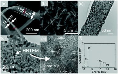
In the past, the vast majority of PbO nanostructures have been obtained exclusively from solution.14–21 Recently we have tried to grow PbO2 NWs via the VLS mechanism and the reaction of Pb with O2 at 800 °C and 10 Pa which are exactly the same growth conditions used to obtain SnO2 NWs.2,3 However we did not obtain any PbO2 NWs due to the fact that PbO2 has a low melting point of 290 °C. Instead, we always obtained PbO layers as it has a higher melting point of 888 °C. We tried to promote the growth of PbO NWs by using different catalysts, such as Au, Ni or Mo or by reducing the temperature from 800 °C down to 700 °C, 600 °C and 500 °C, keeping everything else equal, but one-dimensional growth did not occur. This was attributed to the fact that Pb readily dissolves Au and forms PbAu225,26 but also that the liquid particles of Pb have a small surface tension at elevated temperatures, which prohibits the formation of well-defined particles, which are essential for VLS growth. Consequently, here we have tried to promote the growth of PbO NWs at lower temperatures i.e. 200 °C, 300 °C and 400 °C while maintaining Pb at 800 °C and 10 Pa in order to provide an adequate flux of Pb under a flow of Ar and O2.In this case, the reaction of Pb and O2 readily leads to the one-dimensional growth of PbO NWs at 200 °C even without the use of a catalyst. A typical SEM image of the PbO NWs is shown in Fig. 1(a)–(c). These have the form of tapes with a thickness of 20 nm, a width of 150 nm, and a length of up to 100 μm. However, it is apparent that the width is not uniform along their length and one may observe a tendency towards branching leading to the formation of jagged edges. The TEM and HRTEM images of the PbO NWs are shown in Fig. 1(d) and (e) from which we find that they consist of mixed orthorhombic and tetragonal PbO. Moreover, PbO is Pb-rich as determined from EDX analysis as shown in Fig. 1(f).
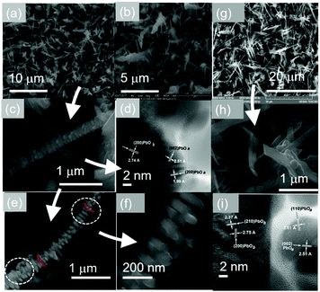
Similar PbO nanostructures were obtained at 300 °C as shown in Fig. 2(a)–(c) which also consist of orthorhombic and tetragonal PbO as verified by the HRTEM image in Fig. 2(d). However, we also observed the occurrence of interconnected rods forming chains as shown in Fig. 2(e) and (f). The formation of these PbO nanostructures with a mixed orthorhombic and tetragonal crystal structure was reproducible as shown in Fig. 2(g)–(i).
It should be emphasized that the reaction of Pb with O2 did not lead to the one-dimensional growth of PbO2 at 200 °C despite the fact that PbO2 has a melting point of 290 °C. This is in contrast to the findings of Pan et al.22 who obtained PbO2 NWs by physical vapor deposition using PbO at 950 °C and 40 kPa under an inert gas flow of Ar. The PbO2 NWs of Pan et al.22 were collected on 10 mm × 60 mm Al2O3 at lower temperatures that were not specified. We tried to grow PbO2 NWs between 200 °C and 400 °C by using PbO and PbO2 at 800 °C and 10 Pa but we always obtained PbO.
This is consistent with the fact that PbO2 is not a stable oxide and will be converted into PbO by heating up to 400 °C.
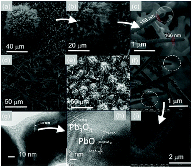
In addition to the above, we observed the formation of urchin-like structures at 400 °C as shown in Fig. 3(a) and (b). A close up of these structures is shown in Fig. 3(c) from which one may readily observe the formation of particles on the ends of the PbO NWs. The particles were found to consist of Pb and Au by using EDX and the same kind of nanostructures were obtained upon repeating the growth as shown in Fig. 3(d)–(f). It is reasonable then to suggest that the one dimensional growth occurs at 400 °C via a self-catalysed VLS mechanism as we observed particles on the ends of the PbO NWs.29
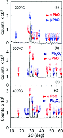
All of the PbO nanostructures obtained at 200 °C exhibited clear and well resolved peaks in the XRD as shown in Fig. 4 corresponding to the orthorhombic and tetragonal crystal structure of PbO consistent with what was observed from the HRTEM image. The PbO obtained at 300 °C consists mainly of orthorhombic and tetragonal PbO but one may also observe some minor peaks belonging to Pb3O4 that are stronger at 400 °C, but we did not detect any peaks belonging to PbO2.
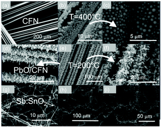
Besides changing the temperature, we found that the morphology of PbO can be tailored in a reproducible and systematic fashion by changing the pressure. We obtained well defined, faceted particles of PbO between 200 °C and 500 °C at 1Pa as shown in Fig. 5. This occurs due to the higher flux of Pb that arrives on the surface of Si and f-SiO2. In contrast, we observe the formation of two-dimensional (2D) PbO between 200 °C and 500 °C at 1 kPa, as shown in Fig. 5. Consequently, it is possible to tune the morphology by changing the growth conditions but the one-dimensional growth only occurs in a relatively narrow window of growth conditions, i.e. between 200 and 300 °C at 10−1 mbar. PbO NWs were also grown on CFNs consisting of carbon fibers with an average diameter of 8 μm as shown in Fig. 6.
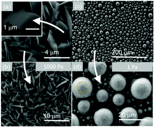 | ||
| Fig. 5 (a and b) SEM images of plate like PbO obtained at 10 mbar; (c and d) spherical particles of PbO with diameters up to 10 μm obtained at 1 Pa. | ||
CFNs have a metallic like conductivity which is particularly important for the realization of advanced LABs as the overall resistance of a cell needs to be as small as possible. Furthermore, PbO NWs were grown directly over SnO2 NWs as shown in Fig. 6(h) and (i), thereby increasing the surface area, which is desired in energy storage. However, before discussing how the SnO2/PbO NWs may be converted into SnO2/PbO2 branched NWs, which is important for energy storage and the realization of advanced LABs, it is useful to consider first the properties of the SnO2/PbO heterojunction by DFT calculations of the electronic structure and in particular the specific band line up, which is important for energy conversion i.e. solar cells and the photocatalytic generation of hydrogen and oxygen.
3.2. Electronic properties of the PbO/SnO2 heterojunction
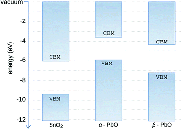
In the past, PbO has been deposited on TiO2 for the photodegradation of CH3(CH2)16COOH by Bhachu et al.13 who confirmed theoretical predictions suggesting that PbO on TiO2 behaves as an active visible light photocatalyst through the formation of new electronic states above the valence band maximum in TiO2 which in turn results in the efficient separation of electron–hole pairs, holes being localized in the PbO and electrons in TiO2. Similarly, the visible light absorption and photocurrent properties of PbO on ZnO NWs have been investigated by Shi et al.30 who suggested that a type II band alignment exists between PbO and ZnO. More importantly, Lim et al.31 investigated the properties of layered SnO and PbO separately from one another and found that SnO,32 which is a p-type semiconductor with an indirect energy band gap of 0.7 eV, is better for electron transfer and hydrogen evolution than PbO. Recently we have carried out a detailed theoretical investigation into the properties of the SnO/PbO heterojunction and showed that it has a broken-gap type II band line up which is very attractive indeed for the photocatalytic dissociation of water.4 On the other hand SnO2 has attracted a great deal of attention as an electron transport layer due to its higher electron mobility, better stability against exposure to UV, and better band alignment compared with other oxides such as TiO2.33 Before elaborating further, it is useful to mention that Butler et al.34 investigated theoretically the properties of an ultrathin layer of PbO2 on SnO2 and showed that it may be used to tune the work function of SnO2 and achieve energy levels commensurate with important technological materials for energy conversion. To the best of our knowledge, no one has investigated the properties of the SnO2/PbO heterojunction, which is interesting not just from a fundamental point of view but also from a technological point of view.The electronic properties of litharge α-PbO, massicot β-PbO and SnO2 were examined by DFT calculations using the CASTEP code.35–37 The structures are shown in Fig. 7(a), 8(a) and 9(a). The geometrical optimization of the structures was carried out in the generalized gradient approximation (GGA) using the Perdew, Burke and Ernzerhof (PBE)38 density functional with ultrasoft potentials. For the PbO structures, the semi-empirical dispersion correction scheme Tkatchenko–Scheffler39 was applied, in order to account for the dispersion forces in the layered systems of α-PbO and β-PbO. The effect of the spin orbit coupling has been neglected as it is expected to be minimal.40 In our calculations, the unit cell was optimized with a 7 × 7 × 7 k-point grid and a cut-off energy of the plane wave basis at 600 eV. The calculated structural properties are listed in Table 1 along with experimental values.41–43 The calculations are close to the experimental values, with the Tkatchenko–Scheffler correction describing better the interlayer distances. For the calculation of the electronic properties and density of states (DOS) we used the computationally demanding hybrid functional PBE044,45 for better accuracy than the GGA level of theory. The cut off energy of the plane waves, for the DOS calculation, was set at 800 eV. The band structures and the p-DOS calculations performed for the primitive cells are shown in Fig. 7–9. The litharge structure of PbO presents an indirect band gap between the Γ and M points calculated using the PBE0 functional at 1.9 eV, identical to the reported experimental values.41,42 The massicot structure of PbO has an indirect gap of 2.86 eV, in close agreement with the experimental values of 2.67 and 2.8.42,43 Finally, the SnO2 band gap (Fig. 9) is calculated using the PBE0 functional at 3.18 eV which is slightly underestimated when compared with the experimental value of 3.6 eV.46
 | ||
| Fig. 9 (a) SnO2 structure, (b) DFT calculations of the band structure using the PBE0 hybrid functional; and (c) DFT calculations of the density of states (DOS) using PBE0. | ||
| a (Å) | b (Å) | c (Å) | XC functionals | |
|---|---|---|---|---|
| α-PbO | 4.059 | 4.059 | 5.579 | PBE–GGA |
| 4.066 | 4.066 | 5.286 | PBE–vdW (TS) | |
| 3.976 | 3.976 | 5.023 | Experiment | |
| β-PbO | 4.851 | 5.746 | 6.181 | PBE–GGA |
| 4.810 | 5.800 | 6.007 | PBE–vdW (TS) | |
| 4.755 | 5.489 | 5.891 | Experiment | |
| SnO2 | 4.820 | 4.820 | 3.234 | PBE–GGA |
| 4.731 | 4.731 | 3.189 | experiment |
For the calculation of the work function, we have performed DOS calculations using supercells of 8 layers (8 × 1 × 1) and a vacuum of ∼20 Å. The electrostatic potential was calculated using the c2x tool47 and the vacuum energy level was extracted. Then, the work function was calculated as: W = Vvac − EFermi.
The calculations are shown in Table 2. The values are close to the experimental ones reported. Slight variations are expected due to limitations of the DFT method such as the nature of the calculated structure, i.e., no defects are present in the simulations. According to these calculations, the band alignment between SnO2 and PbO shows a type-II heterostructure. The alignment of the energy levels is shown in Fig. 10.
| Calculated band gap (eV) | Calculated work function (eV) | |
|---|---|---|
| SnO2 | 3.18 | 7.49 |
| α-PbO | 1.89 | 4.58 |
| β-PbO | 2.86 | 4.73 |
3.3. Conversion of SnO2/PbO into SnO2/PbO2 nanowires for energy storage
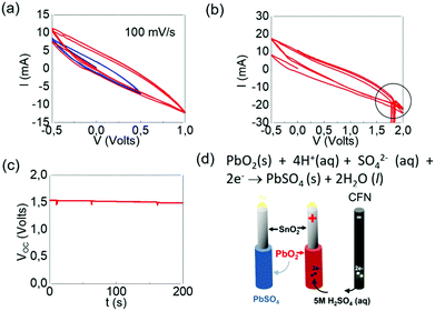
Despite the fact that we did not obtain any PbO2 NWs by the VLS mechanism one may easily convert PbO into PbO2 NWs in an electrochemical fashion. A LAB half-cell consisting of a SnO2/PbO NW anode and a CFN cathode in 5 M H2SO4(aq) was set-up. The standard reduction potential of the reaction PbO (s) + 2H+ (aq) + 2e− → Pb (s) + H2O (l) is −0.44 V and no reaction occurs between CFN and 5 M H2SO4 (aq). Hence, this half-cell has a standard total potential of only −0.44 V. A typical CV curve from the SnO2/PbO core–shell NWs versus a CFN in 5M H2SO4 (aq) is shown in Fig. 11(a). We do not observe any reduction or oxidation. However, the conversion of PbO into PbO2 may be observed in Fig. 11(b) with the appearance of narrow peaks at ∼1.8 Volts. The open circuit potential of the resultant SnO2/PbO2 NWs i.e. VOCversus time is shown in Fig. 10(c) and is equal to 1.6 Volts, which is very close to the standard reduction potential of PbO2. For completeness, the reaction that occurs upon discharging is shown in Fig. 10(d). In short, although we did not obtain any PbO2 NWs by the VLS mechanism, it is evident that PbO NWs can be grown on the CFNs and SnO2 NWs, after which they may be converted into PbO2 for energy storage and the realization of advanced LABs.Finally, it is useful to point out that PbO/SnO2 NWs can be converted into PbI2/SnO2 NWs by exposure to iodine after which they may be converted into methyl ammonium lead iodide CH3NH3PbI3/SnO2 NWs via immersion in a solution of methyl ammonium iodide (MAI), i.e. CH3NH3I. In the past, PbO has been deposited on TiO2/Sn:In2O3 and converted in this way into CH3NH3PbI3i.e. methyl-ammonium-lead-iodide (MAPI).48–50 The conversion of PbO/SnO2 NWs into branched CH3NH3PbI3/SnO2 NWs is therefore attractive for the realization of perovskite solar cells where the n-type SnO2 NWs act as one-dimensional pathways for the extraction of the photogenerated electrons in the CH3NH3PbI3.48
4. Conclusions
We have carried out a detailed investigation into the growth of PbO NWs via the reaction of Pb with O2 between 200 °C and 400 °C at 10 Pa on Si (001) and f-SiO2. The one dimensional growth occurs only at low temperatures between 200 °C and 300 °C in which case we obtained PbO NWs in the form of tapes with a thickness of ∼20 nm, a width of ∼150 nm, and a length up to ∼100 μm. The PbO NWs have a mixed orthorhombic and tetragonal crystal structure but we did not obtain any PbO2 irrespective of the growth temperature, pressure, etc. One dimensional growth occurs via a self-catalyzed VLS mechanism that was suppressed at temperatures above 500 °C. In addition, the morphology of the PbO was tuned in a reproducible fashion by varying the pressure, in which case we obtained two dimensional plates at 1 kPa and well-defined particles with a diameter of up to 10 μm at 1 Pa. We show that the PbO/SnO2 may be easily converted into SnO2/PbO2 NWs for energy storage and the realization of advanced LABs, but also that PbO/SnO2 NWs have a type II band alignment which is attractive for photocatalysis and energy conversion.Author contributions
M. Z.: conceptualization, experimental work and writing; N. K. and N. N. L.: computational work and writing; A. C.: review and editing; E. T. and E. V.: experimental work and analysis.Conflicts of interest
There are no conflicts to declare.Acknowledgements
The authors N. K. and N. N. L. acknowledge support by the projects (1) “nanoporous GrAphene membrane made without TransfEr for gas Separation-GATES” (MIS 5041612), and (2) “National Infrastructure in Nanotechnology, Advanced Materials and Micro-Nanoelectronics” (MIS 5002772), both funded by the Operational Program “Competitiveness, Entrepreneurship and Innovation” (NSRF 2014-2020), co-financed by Greece and the European Union (European Regional Development Fund).References
- X. Huang, H. Wang, C. Niua and A. Rogach, CrystEngComm, 2015, 17, 5593 RSC.
- D. Tsokkou, A. Othonos and M. Zervos, Appl. Phys. Lett., 2012, 100, 133101 CrossRef.
- M. Zervos, A. Othonos, E. Tanasu and E. Vasille, J. Phys. Chem. C, 2018, 122(39), 22709 CrossRef CAS.
- M. Zervos, N. Lathiotakis, N. Kelaidis, A. Othonos, E. Tanasu and E. Vasille, Nanoscale Adv., 2019, 1, 1980 RSC.
- M. Zervos, C. Mihailescu, J. Giapintzakis, C. Luculescu, N. Florini, P. Komninou, J. Kioseoglou and A. Othonos, APL Mater., 2014, 2, 0561041 CrossRef.
- A. Charalampous, M. Zervos, J. Kioseoglou, K. Tsagaraki, M. Androulidaki, G. Konstantinidis, E. Tanasă and E. Vasile, ACS Appl. Energy Mater., 2019, 2(6), 4274–4283 CrossRef CAS.
- S. J. Pearton, J. Yang, P. H. Cary IV, F. Ren, J. Kim, M. J. Tadjer and M. A. Mastro, Appl. Phys. Rev., 2018, 5, 011301 Search PubMed.
- A. Othonos, M. Zervos and C. A. Christofides, Appl. Phys., 2010, 108, 124319 Search PubMed.
- D. Scanlon, A. B. Kehoe, G. W. Watson, M. O. Jones and W. I. F. David, et al. , Phys. Rev. Lett., 2011, 107, 246402 CrossRef PubMed.
- M. Zervos, A. Othonos, E. Tanasa, E. Vasile and E. Leontidis, J. Phys. Chem. C, 2018, 122, 25813–25821 CrossRef CAS.
- O. Semeniuk, O. Grynko, G. Decrescenzo, G. Juska, K. Wang and A. Reznik, Sci. Rep., 2017, 7, 8659 CrossRef CAS PubMed.
- S. K. Hyun, G. J. Sun, J. K. Lee, C. Lee, W. I. Lee and H. W. Kim, Thin Solid Films, 2017, 637, 21 CrossRef CAS.
- D. S. Bhachu, S. Sathasivam, C. J. Carmalt and I. P. Parkin, PbO-Modified TiO2 Thin Films: A Route to Visible Light Photo Catalysts, Langmuir, 2014, 30, 624 CrossRef CAS PubMed.
- L. Shi, Y. Xu and Q. Li, Cryst. Growth Des., 2008, 8, 3521 CrossRef CAS.
- L. X. Ding, F. L. Zheng, J. W. Wang, G. R. Li and Z. L. Wang, et al. , Chem. Commun., 2012, 48, 1275 RSC.
- C. Z. Yao, Y. X. Tong, H. X. Ma, Q. J. Gong, L. X. Meng, J. H. Yao and D. C. Xia, J. Electrochem. Soc., 2010, 157, 503 CrossRef.
- M. Bervas, M. Perrin, S. Geniès and F. Mattera, J. Power Sources, 2007, 173, 570 CrossRef CAS.
- R. Inguanta, Z. S. Piazza and C. Sunseri, J. Electrochem. Soc., 2008, 155, 205 CrossRef.
- P. Perret, T. Brousse, D. Bélanger and D. Guay, ECS Trans., 2009, 16, 207 CrossRef CAS.
- P. Perret, T. Brousse, D. Bélanger and D. Guaya, J. Electrochem. Soc., 2009, 156, 645 CrossRef.
- C. J. Yang and S. M. Park, Electrochim. Acta, 2013, 108, 86 CrossRef CAS.
- Z. W. Pan, Z. R. Dai and Z. L. Wang, Appl. Phys. Lett., 2002, 80, 309 CrossRef CAS.
- M. Zervos, A. Othonos, E. Tanasa and E. Vasile, J. Phys. Chem. C, 2019, 123, 16415 CrossRef CAS.
- J. Berashevich, J. Rowlands and A. Reznik, J. Phys.: Condens. Matter, 2013, 25, 475801 CrossRef CAS PubMed.
- T. Tamaka, M. Nakamoto, R. Oguni, J. Lee and S. Hara, Z. Metallkd., 2004, 95, 818 CrossRef.
- K. N. Tu and D. A. Chance, J. Appl. Phys., 1975, 46, 3229 CrossRef CAS.
- A. Moncada, S. Piazza, C. Sunseri and R. Inguanta, J. Power Sources, 2015, 275, 181 CrossRef CAS.
- R. Kumar, K. N. Rao, K. Rajanna and A. R. Phani, Mater. Res. Bull., 2014, 52, 167–176 CrossRef CAS.
- R. L. Oliveri, M. G. Insinga, S. Pisana, B. Patella, G. Aiello and R. Inguanta, Appl. Sci., 2021, 11(14), 6357 CrossRef CAS.
- J. Shi, P. Guo, Y. Liu, J. Su and L. Guo, J. Mater. Res., 2016, 31(11), 1622–1630 CrossRef CAS.
- C. S. Lim, Z. Sofer, O. Jankovsky, H. Wanga and M. Pumera, RSC Adv., 2015, 5, 101949 RSC.
- H. Peng, A. Bikowski, A. Zakutayev and St. Lany, APL Mater., 2016, 4, 106103 CrossRef.
- Q. Jiang, Z. Zhang and J. You, Small, 2018, 14, 1801154 CrossRef PubMed.
- K. T. Butler, J. Buckeridge, C. Richard, A. Catlow and A. Walsh, Phys. Rev. B, 2014, 89, 115320 CrossRef.
- T. Arias, M. C. Payne and J. D. Joannopoulos, Phys. Rev. Lett., 1992, 69, 1077–1080 CrossRef CAS PubMed.
- M. C. Payne, M. P. Teter, D. C. Allan, T. A. Arias and J. D. Joannopoulos, Rev. Mod. Phys., 1992, 64, 1045 CrossRef CAS.
- M. D. Segall, et al. , J. Phys.: Condens. Matter, 2002, 14, 2717 CrossRef CAS.
- J. Perdew, K. Burke and M. Ernzerhof, Phys. Rev. Lett., 1996, 77, 3865 CrossRef CAS PubMed.
- A. Tkatchenko and M. Scheffler, Phys. Rev. Lett., 2009, 102, 073005 CrossRef PubMed.
- A. Bakhtatou and F. Ersan, Phys. Chem. Chem. Phys., 2019, 21, 3868 RSC.
- B. Thangaraju and P. Kaliannan, Semicond. Sci. Technol., 2000, 15, 542 CrossRef CAS.
- R. C. Keezer, D. L. Bowman and J. H. Becker, J. Appl. Phys., 1968, 39, 2062 CrossRef CAS.
- L. M. Droessler, PhD thesis, University of Oxford, 2014.
- C. Adamo and V. Barone, J. Chem. Phys., 1999, 110, 6158 CrossRef CAS.
- M. Erzenhof and G. E. Scuseria, J. Chem. Phys., 1999, 110, 5029 CrossRef.
- Y. Hinuma, T. Toyao, T. Kamachi, Z. Maeno, S. Takakusagi, S. Furukawa, I. Takigawa and K.-I. Shimizu, J. Phys. Chem. C, 2018, 122, 29435–29444 CrossRef CAS.
- M. J. Rutter, Comput. Phys. Commun., 2018, 225, 174–179 CrossRef CAS.
- J. Huang, K. Jiang, X. Cui, Q. Zhang, M. Gao, M. Su, L. Yang and Y. Song, Sci. Rep., 2015, 5, 15889 CrossRef CAS PubMed.
- X. P. Cui, K. J. Jiang, J. H. Huang, X. Q. Zhou, M. J. Su, S. G. Li, Q. Q. Zhang, L. M. Yanga and Y. L. Song, Chem. Commun., 2015, 51, 1457–1460 RSC.
- J. H. Im, J. Luo, M. Franckevicius, N. Pellet, P. Gao, T. Moehl, S. M. Zakeeruddin, M. K. Nazeeruddin, M. Grätzel and N. G. Park, Nano Lett., 2015, 15, 2120–2126 CrossRef CAS PubMed.
| This journal is © The Royal Society of Chemistry 2022 |

