 Open Access Article
Tolerance of metal halide perovskites to mechanical treatment enables the fabrication of patterned luminescence nano- and microstructures
Jun
Li
 a,
Aymen
Yangui
a,
Reza
Jafari Jam
b,
Qingzhi
An
c,
Yana
Vaynzof
a,
Aymen
Yangui
a,
Reza
Jafari Jam
b,
Qingzhi
An
c,
Yana
Vaynzof
 *c,
Eva
Unger
 ad,
Ivan
Maximov
 b and
Ivan G.
Scheblykin
 *a
*a
aDivision of Chemical Physics and NanoLund, Lund University, Box 124, 22100, Lund, Sweden. E-mail: ivan.scheblykin@chemphys.lu.se
bDivision of Solid State Physics and NanoLund, Lund University, Box 118, 22100, Lund, Sweden
cIntegrated Center for Applied Physics and Photonic Materials and the Center for Advancing Electronics Dresden (cfaed), Technische Universität Dresden, Nöthnitzer Straße 61, 01187 Dresden, Germany. E-mail: yana.vaynzof@tu-dresden.de
dHelmholtz-Zentrum Berlin für Materialien und Energie GmbH, HySPRINT Innovation Lab: Hybrid Materials Formation and Scaling, Kekuléstraße 5, 12489 Berlin, Germany
First published on 20th October 2022
Abstract
Metal halide perovskites have shown a great performance in a broad range of optoelectronic devices. The variety of preparation methods makes perovskites especially attractive, yet preparation of complex nanostructures based on these materials remains challenging. Here we present a template assisted method allowing to achieve any pre-designed arrangement of methylammonium lead triiodide (MAPbI3) polycrystalline patterns with the spatial resolution defined by the template. We utilized a Si/SiO2 wafer with circular 180 nm deep recesses with diameters ranging from 200 to 1600 nm as a template. A polycrystalline perovskite powder was obtained by scratching off a thin perovskite film and mechanically introduced into the patterned template as a pigment. Scanning electron microscopy revealed that the recesses are filled with tightly packed sub-20 nm crystallites. Considering that the spin-coated film used as a source of MAPbI3 consisted of grains up to 2000 nm in diameter suggests that the initially prepared grains were crashed by rubbing to much smaller crystallites. In spite of this harsh mechanical treatment, the filled recesses showed a strong photoluminescence signal, demonstrating the applicability of this approach for the fabrication of diverse nanophotonic structures.
1 Introduction
Metal halide perovskites (MHPs) have shown an excellent performance in solar cells and other optoelectronic applications.1–3 One of the key advantages of MHPs as compared with other semiconductors is that they can be processed from solution,4 which offers a great flexibility in designing the morphology of the material at nano-scale.5 For example, one can fabricate polycrystalline MHP films via spin-coating and inkjet printing,6 and prepare MHP materials such as nanocrystals (quantum dots)2 and nanowires.7Recently, significant research efforts have been dedicated to the fabrication of patterned perovskite structures which is extremely important for many applications.5 The currently existing methods can be roughly divided to template patterning, inkjet printing, and laser patterning.5 Template patterning uses complex multistep protocols based on lithography and other traditional techniques of semiconductors industry to grow (or transfer) the MHP material or precursors to the desired locations.5,8 MHPs nanowire array devices can be prepared by controlling the template-assisted crystallization growth of MHPs on a substrate.7,9–11 Local laser ablation and multiplexed cantilever assisted methods were also applied to the preparation of individual MHPs crystal array devices with variable sizes from 1 to 50 μm.12,13 All these methods are rather complicated, often not easily upscaled and usually possessing a limited spatial resolution for the resulting structures.
In this study, we present a very simple template-assisted method allowing to create any pre-desired pattern with accuracy on the level of tens of nanometres filled with methylammonium lead triiodide (MAPbI3) polycrystalline material. Here we use the ancient technology of colouring by mechanical rubbing of a dry pigment into the surface of the material which contains nano/microcavities allowing for the mechanical adsorption of the pigment. Surprisingly, MAPbI3 semiconductor survives such a rough mechanical treatment and not only can be rubbed into any nanostructured surface as a dry pigment, but also, due to defect tolerance and possibly self-healing, does not lose (or quickly recovers) its electronic properties14–16 as revealed by strong photoluminescence (PL).
To demonstrate the method, we prepared Si/SiO2 substrates with different circular recesses (which will be called holes hereafter) with diameters 200, 400, 800 and 1600 nm and depth of approximately 140 nm. The patterning of the structure was made using electron beam lithography (EBL) and reactive ion etching (RIE) of the top SiO2 layer. As a substrate for EBL we used a thermally oxidized Si wafer with the spin-coated electron beam sensitive resist AR-6200-09. The EBL exposure was performed in Voyager lithography system (Raith GmbH, Germany) with a 50 keV electron beam. After the exposure and resist development, we etched ≈140 nm of the top SiO2 layer (the total thickness of the SiO2 layer was 180 nm) in a table top RIE tool (Sirus T2, Trion Technology, USA). The remaining resist served as an etch mask during the 480 s long RIE CHF3 process at the pressure of 20 mTorr. To remove the resist after etching and clean the substrate surface, the wafer was washed in Remover 1165 (Shipley, USA) and isopropanol and blown dry in nitrogen.
MAPbI3 perovskite thin film was fabricated by spin-coating technique in a dry box (RH < 1%) according to the procedure described in detail elsewhere.17 In brief, the perovskite solution (40% wt) was prepared with 1![[thin space (1/6-em)]](https://www.rsc.org/images/entities/char_2009.gif) :
:![[thin space (1/6-em)]](https://www.rsc.org/images/entities/char_2009.gif) 3 molar ratio of lead acetate trihydrate and methylammonium iodide dissolved in dimethylformamide. 8‰ amount of hypophosphorous were also added into the perovskite precursor. The film was prepared by spin-coating the precursor solution at 2000 rpm for 60 s on glass substrates, followed by 25 s dry air blowing, 5 min room temperature drying and 10 min annealing at 100 °C.
3 molar ratio of lead acetate trihydrate and methylammonium iodide dissolved in dimethylformamide. 8‰ amount of hypophosphorous were also added into the perovskite precursor. The film was prepared by spin-coating the precursor solution at 2000 rpm for 60 s on glass substrates, followed by 25 s dry air blowing, 5 min room temperature drying and 10 min annealing at 100 °C.
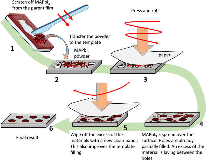
The procedure of filling the patterned template with the MAPbI3 pigment is described in detail in Fig. 1. The perovskite material was manually scratched off a glass substrate (step 1) and the resulting powder was collected on the templated substrate (step 2). Then, an ordinary printing paper was used to rub in the perovskite pigment into the template (step 3). This procedure allowed for filling most of the holes etched on the surface with MAPbI3, however, the space between the holes was also contaminated by the material. To remove the unwanted material and further improve the hole filling another piece of clean paper of the same type was used to wipe the substrate (step 5). The whole procedure was carried out in ambient air with RH of about 40%. We note that the procedure might generate small Pb-containing particles, however from our experience these strongly adhere to the paper, thus not generating obvious dust or contamination. Nonetheless, standard precautions such as wearing gloves and safety googles are advised.
There are several advantages to this method, as compared to attempting to directly form perovskite crystals in the pre-patterned templates. First of all, in the case of the latter, it is unlikely that the perovskite precursor solution would fill the small recesses of the template, thus leading to a formation of a film above them, rather than their filling. Secondly, a direct fabrication would make it necessary to anneal the perovskite, making it incompatible with temperature sensitive substrates. On the other hand, the method proposed here can be easily applied to a range of different substrates with different patterns and structures, very similar to traditional coloring techniques using solid pigments.
Considering that PL is an excellent probe for the optoelectronic properties of perovskite samples,18–20 we studied their PL using a wide-field fluorescence microscope. It is based on Olympus IX71 with a 40× objective lens (Olympus LUCPlanFL, NA = 0.6) where Argon-ion (514 nm, CW) laser is used as an excitation source and ProEM 512B CCD camera (Princeton Instruments) as a detector. One pixel on the CCD chip corresponds to 200 nm in the sample plane while the diffraction limit of the image resolution for the wavelength of MAPbI3 emission is around 800 nm (4 pixels). The excitation power density at the sample plane was approximately 0.2 W cm−2. The microscope also allows measuring PL spectra using a transmission diffraction grating. We also used a Hitachi SU8100 scanning electron microscope (SEM) to characterize the sample.
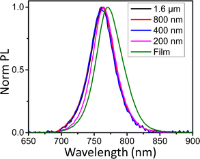
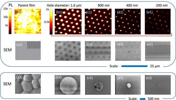
Fig. 2 shows the PL and SEM images of the samples prepared by the rubbing method. For PL imaging the samples were placed in a nitrogen atmosphere. Orderly arranged individual bright spots are observed under laser illumination as shown in Fig. 2(b–e). Bright PL was observed from most of the holes meaning that most of them were successfully filled with MAPbI3. Moreover, the spectrum of PL from all holes (Fig. 3) – independent on their size – has its maximum at 750 nm which is very close to 760 nm expected from a bulk perovskite film confirming that the holes are indeed filled with MAPbI3 despite these harsh mechanical manipulations.
 | ||
| Fig. 3 PL spectra of MAPbI3 crystals pasted to recesses of different sizes in comparison with PL spectra of the MAPbI3 film. | ||
SEM analysis of the samples shows that most of the holes are at least partially filled with the perovskite material. The least efficient filling is observed for the smallest holes, which is to be expected considering the large surface roughness of the paper used for rubbing the perovskite material into the ordered arrays of holes. It is obvious that using industry-standard rubbing methodologies, which are known for coloring and other purposes for hundreds of years, should be able to improve the filling up to perfection.
The SEM image Fig. 2(b3) shows that the MAPI3 material pasted into the holes consists of very small grains, which are better resolved in the SEM images in Fig. 4. It is evident that most of the grains are smaller than 20 nm. This observation allows us to suggest that the observed 10 nm blue shift of the PL spectrum in comparison with the bulk MAPbI3 film originates from a partial quantum confinement of charge carriers in such small nanocrystals.12 Another possible reason for the spectral shift is a difference in the level of the crystal strain21 between MAPbI3 film and mechanically prepared MAPbI3 small nanocrystals.
It is known that MAPbI3 perovskite is a relatively soft and deformable material with Young's modulus value 14 GPa and rather low hardness (resistance of the material to plastic deformation) around 0.6 GPa.22 Therefore, it is not a surprise that when transferring MAPbI3 from the film into Si/SiO2 substrates, a hard paper can break the large grains into small crystals. Note that the procedure did not lead to scratching of the SiO2 surface. However, it is still surprising that the large MAPbI3 grain with the sizes of 500–2000 nm (Fig. 2a1 and a2) of the parent film can be broken into 10–30 nm size crystals using such a simple method. It means that MAPbI3 crystals are brittle and have a tendency to break to a large number of small crystallites. A possible reason for this might be related to the presence of strain inside the MAPbI3 crystals. When an external mechanical force is locally applied to a material with a high local internal stress, it breaks to many small pieces. A well-known example of such a material is tempered or hardened glass, which is used in cars and houses for safety reasons. A key aspect in the production of tempered glass is the fast-cooling stage which makes the surface hard, but creates stress between the surface and the bulk material, which in turn, leads to this specific breaking pattern. So, in analogy to this, we propose that MAPbI3 crystals collapse into small tens of nanometres sized crystallites due to the high local internal strain created during its fabrication.
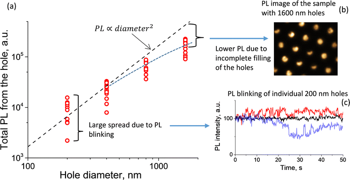
The most important results our study is the demonstration that the PL of the perovskite semiconductor was not completely quenched after its crystals were treated in a harsh mechanical way. We can estimate the difference in PL quantum yield (PLQY) between the parent thin film and the perovskite pigment in the holes. The intensity level we see in the PL images is the counts per pixel of the CCD camera. Images of the holes that are much larger than the resolution of the microscope (the resolution limit is 800 nm) can be directly compared with the PL image of the film. However, if the emitter is smaller than the diffraction limit of the optical resolution, the PL intensity per pixel goes down with the object size decrease. This is because regardless of the actual size of the object, it always appears on the CCD as a diffraction-limited spot of the same size. That is why the samples with 800, 400 and 200 nm holes show a gradual decrease of the PL intensity; yet this observation does not at all mean that their PLQY decreases. To quantitively verify this, we plotted the overall PL intensity measured on individual holes as a function of hole diameter (Fig. 5a). The dependence is close to the one expected for the case of constant PLQY and constant thickness of the perovskite layers. The small deviation observed for large hole diameters is mostly associated with an incomplete hole filling, as is illustrated in Fig. 5b. On the other hand, the large scatter of the data for the small holes (200 nm) is strongly impacted by the PL fluctuations due to PL blinking (Fig. 5c).18,23 We note that the difference in light outcoupling may also impact the results, since it is expected to be more efficient for small holes.24
By examining the signal of the 1.6 μm holes which are larger than the microscope resolution, we are able to truly estimate the impact of the material processing on its PLQY. Intensity per pixel for the 1.6 μm holes is about 10 times lower than that for the parent film (compare images a1 and b1 in Fig. 2 and the corresponding intensity scales). It means that the PLQY of the MAPbI3 rubbed into the template is decreased by approximately a factor of 10 in comparison with the parent high-quality film. In this simple comparison we do not account for the difference between the film thickness (≈260 nm) and the depth of the holes (140 nm) since the absorption length (100 nm at 514 nm) is smaller than both these values, so at first approximation all light is absorbed in both cases. The decrease of PLQY is most likely associated with the formation of crystal defects during the mechanical treatment, considering that via this process the surface to bulk ratio was increased by a factor of 50 (decreasing the size from 1000 nm to approximately 20 nm). However, despite this harsh mechanical treatment, the preservation of the PL suggests perovskites are rather tolerant to such processes either as part of their defect tolerance or due to their ability to recover, at least partially, its properties in a short timespan due to self-healing.14–16 A detailed spectroscopic investigation will be carried out in the future. Note that all manipulations with the perovskite were carried out in ambient air, therefore, it is not excluded that our method realized in an inert atmosphere can give a better result in terms of higher PL quantum yield of the resulted samples.
2. Conclusion
We introduce a simple rubbing method that allows to deposit a polycrystalline metal–halide perovskite into any structured surface of an object of any geometry. This method is the same as traditional mechanical surface colouring with dry pigments. During the deposition initially prepared micrometre-sized perovskite crystals are effortlessly mechanically broken down to small 10–30 nm nanocrystals. We propose that it is due to built-in internal mechanical stress in as synthesised MAPI3 crystals – a property that resembles that of tempered glass. Despite the harsh mechanical treatment, the semiconductor does not lose its electronic properties, exhibiting spectrally similar photoluminescence to that of a high-quality polycrystalline MAPbI3 film. We assign the bright PL signal from crushed crystals to be a result of defect tolerance of MAPbI3. We observe a slight blue-shift of PL, which is attributed to a partial quantum confinement effect in small perovskite grains and a difference in the crystal strain between the film and the grains.Conflicts of interest
There are no conflicts to declare.Acknowledgements
The work was supported by NanoLund (p18-2019) and Swedish Research Council (2020-03530). The authors are thankful to NanoLund and Myfab for financial support to access Lund Nano Lab. J. L thanks the China Scholarship Council (CSC No: 201608530162) for his PhD scholarship. Q. A. and Y. V. thank the center for advancing electronics Dresden (cfaed) for generous funding in the framework of the postdoc program and the Deutsche Forschungsgemeinschaft (DFG) for funding the “PERFECT PVs” project (Grant No. 424216076) via the Special Priority Program 2196.References
- J. Berry, T. Buonassisi, D. A. Egger, G. Hodes, L. Kronik, Y.-L. Loo, I. Lubomirsky, S. R. Marder, Y. Mastai and J. S. Miller, et al., Hybrid Organic–Inorganic Perovskites (HOIPs): Opportunities and Challenges, Adv. Mater., 2015, 27(35), 5102–5112, DOI:10.1002/adma.201502294.
- A. Dey, J. Ye, A. De, E. Debroye, S. K. Ha, E. Bladt, A. S. Kshirsagar, Z. Wang, J. Yin and Y. Wang, et al., State of the Art and Prospects for Halide Perovskite Nanocrystals, ACS Nano, 2021, 15(7), 10775–10981, DOI:10.1021/acsnano.0c08903.
- L. Schmidt-Mende, V. Dyakonov, S. Olthof, F. Ünlü, K. M. T. Lê, S. Mathur, A. D. Karabanov, D. C. Lupascu, L. M. Herz and A. Hinderhofer, et al., Roadmap on Organic–Inorganic Hybrid Perovskite Semiconductors and Devices, APL Mater., 2021, 9(10), 109202, DOI:10.1063/5.0047616.
- Y. Vaynzof, The Future of Perovskite Photovoltaics—Thermal Evaporation or Solution Processing?, Adv. Energy Mater., 2020, 10(48), 2003073, DOI:10.1002/aenm.202003073.
- L. Liang, T. Ma, Z. Chen, J. Wang, J. Hu, Y. Ji, W. Shen and J. Chen, Patterning Technologies for Metal Halide Perovskites: A Review, Adv. Mater. Technol., 2022, 2200419, DOI:10.1002/admt.202200419.
- F. Mathies, E. J. W. List-Kratochvil and E. L. Unger, Advances in Inkjet-Printed Metal Halide Perovskite Photovoltaic and Optoelectronic Devices, Energy Technol., 2019, 8, 1900991, DOI:10.1002/ente.201900991.
- Z. Zhang, K. Suchan, J. Li, C. Hetherington, A. Kiligaridis, E. Unger, I. G. Scheblykin and J. Wallentin, Vertically Aligned CsPbBr 3 Nanowire Arrays with Template-Induced Crystal Phase Transition and Stability, J. Phys. Chem. C, 2021, 125(8), 4860–4868, DOI:10.1021/acs.jpcc.0c11217.
- D. Xing, C. Lin, Y. Ho, A. S. A. Kamal, I. Wang, C. Chen, C. Wen, C. Chen and J. Delaunay, Self-Healing Lithographic Patterning of Perovskite Nanocrystals for Large-Area Single-Mode Laser Array, Adv. Funct. Mater., 2021, 31, 2006283, DOI:10.1002/adfm.202006283.
- W. Deng, J. Jie, X. Xu, Y. Xiao, B. Lu, X. Zhang and X. Zhang, A Microchannel-Confined Crystallization Strategy Enables Blade Coating of Perovskite Single Crystal Arrays for Device Integration, Adv. Mater., 2020, 32, 1908340, DOI:10.1002/adma.201908340.
- M. Spina, E. Bonvin, A. Sienkiewicz, B. Náfrádi, L. Forró and E. Horváth, Controlled Growth of CH3NH3PbI3 Nanowires in Arrays of Open Nanofluidic Channels, Sci. Rep., 2016, 6, 19834, DOI:10.1038/srep19834.
- L. Lee, J. Baek, K. S. Park, Y.-E. Lee, N. K. Shrestha and M. M. Sung, Wafer-Scale Single-Crystal Perovskite Patterned Thin Films Based on Geometrically-Confined Lateral Crystal Growth, Nat. Commun., 2017, 8, 15882, DOI:10.1038/ncomms15882.
- J. S. Du, D. Shin, T. K. Stanev, C. Musumeci, Z. Xie, Z. Huang, M. Lai, L. Sun, W. Zhou and N. P. Stern, et al., Halide Perovskite Nanocrystal Arrays: Multiplexed Synthesis and Size-Dependent Emission, Sci. Adv., 2020, 6, eabc4959, DOI:10.1126/sciadv.abc4959.
- A. Zhizhchenko, S. Syubaev, A. Berestennikov, A. V. Yulin, A. Porfirev, A. Pushkarev, I. Shishkin, K. Golokhvast, A. A. Bogdanov and A. A. Zakhidov, et al., Single-Mode Lasing from Imprinted Halide-Perovskite Microdisks, ACS Nano, 2019, 13(4), 4140–4147, DOI:10.1021/acsnano.8b08948.
- D. R. Ceratti, Y. Rakita, L. Cremonesi, R. Tenne, V. Kalchenko, M. Elbaum, D. Oron, M. A. C. Potenza, G. Hodes and D. Cahen, Self-Healing Inside APbBr3 Halide Perovskite Crystals, Adv. Mater., 2018, 30, 1706273, DOI:10.1002/adma.201706273.
- Y. Yu, F. Zhang and H. Yu, Self-Healing Perovskite Solar Cells, Sol. Energy, 2020, 209, 408–414, DOI:10.1016/j.solener.2020.09.018.
- D. Cahen, L. Kronik and G. Hodes, Are Defects in Lead-Halide Perovskites Healed, Tolerated, or Both?, ACS Energy Lett., 2021, 6(11), 4108–4114, DOI:10.1021/acsenergylett.1c02027.
- V. Swaminathan, J. M. Kalappurakkal, S. B. Mehta, P. Nordenfelt, T. I. Moore, N. Koga, D. A. Baker, R. Oldenbourg, T. Tani and S. Mayor, et al., Actin Retrograde Flow Actively Aligns and Orients Ligand-Engaged Integrins in Focal Adhesions, Proc. Natl. Acad. Sci. U. S. A., 2017, 114(40), 10648–10653, DOI:10.1073/pnas.1701136114.
- A. Merdasa, Y. Tian, R. Camacho, A. Dobrovolsky, E. Debroye, E. L. Unger, J. Hofkens, V. Sundström and I. G. Scheblykin, “Supertrap” at Work: Extremely Efficient Nonradiative Recombination Channels in MAPbI3 Perovskites Revealed by Luminescence Super-Resolution Imaging and Spectroscopy, ACS Nano, 2017, 11(6), 5391–5404, DOI:10.1021/acsnano.6b07407.
- A. Kiligaridis, P. Frantsuzov, A. Yangui, S. Seth, J. Li, Q. An, Y. Vaynzof and I. G. Scheblykin, Are Shockley-Read-Hall and ABC models valid for lead halide perovskites?, Nat. Commun., 2021, 12, 3329, DOI:10.1038/s41467-021-23275-w.
- K. P. Goetz, A. D. Taylor, F. Paulus and Y. Vaynzof, Shining Light on the Photoluminescence Properties of Metal Halide Perovskites, Adv. Funct. Mater., 2020, 30, 1910004, DOI:10.1002/adfm.201910004.
- J. Wu, S.-C. Liu, Z. Li, S. Wang, D.-J. Xue, Y. Lin and J.-S. Hu, Strain in Perovskite Solar Cells: Origins, Impacts and Regulation, Natl. Sci. Rev., 2021, 8(8), nwab047, DOI:10.1093/nsr/nwab047.
- Y. Rakita, S. R. Cohen, N. K. Kedem, G. Hodes and D. Cahen, Mechanical Properties of APbX3 (A = Cs or CH3 NH3; X = I or Br) Perovskite Single Crystals, MRS Commun., 2015, 5(4), 623–629, DOI:10.1557/mrc.2015.69.
- I. G. Scheblykin, Small Number of Defects per Nanostructure Leads to “Digital” Quenching of Photoluminescence: The Case of Metal Halide Perovskites, Adv. Energy Mater., 2020, 10, 2001724, DOI:10.1002/aenm.202001724.
- P. Fassl, V. Lami, F. J. Berger, L. M. Falk, J. Zaumseil, B. S. Richards, I. A. Howard, Y. Vaynzof and U. W. Paetzold, Revealing the Internal Luminescence Quantum Efficiency of Perovskite Films via Accurate Quantification of Photon Recycling, Matter, 2021, 4(4), 1391–1412, DOI:10.1016/j.matt.2021.01.019.
| This journal is © The Royal Society of Chemistry 2022 |


