 Open Access Article
Numerical modeling investigations of the impact of a thin p-type cocatalyst modifier on an n-type photon absorber for unbiased overall solar water splitting†
HanHsuan
Huang
,
Kesiuke
Obata
,
Fuminao
Kishimoto
 and
Kazuhiro
Takanabe
 *
*
Department of Chemical System Engineering, School of Engineering, University of Tokyo, 7-3-1 Hongo, Bunkyo-ku, Tokyo 113-8656, Japan. E-mail: takanabe@chemsys.t.u-tokyo.ac.jp
First published on 20th October 2022
Abstract
Surface modifications of semiconductor photoelectrodes are often introduced to enhance charge separation and reaction kinetics during solar-driven water splitting. Examples include the formation of n–n heterojunctions and the deposition of electrocatalyst layers. The internal electric field in a p–n junction is expected to be stronger than that in an n–n junction, and several studies have used p-type semiconducting electrocatalyst decoration to improve the overall performance of water splitting. However, a design guideline for the p-type modification layer has not been clearly reported. Therefore, we numerically investigated the impact of a thin p-type modification layer on the photoelectrochemical performance of an n-type photoanode. The key parameters were varied in simulations, including the band position, dopant densities, thickness of the p-type layer, and the dopant densities in the n-type region. Our numerical simulations show that the depletion depths in the p-type modification layer and n-type photon absorber are the key characteristics that need to be tuned, which is mainly achieved by controlling the dopant densities. This work also discusses the critical distinction of a p–n heterojunction compared to an n–n heterojunction photoanode.
Introduction
There are concerns about the depletion of fossil fuels, the increase in global energy demands, and environmental pollution. Therefore, recent research efforts have been dedicated to exploring green and clean energy sources in order to develop a sustainable society. Solar energy is the most abundant and promising renewable energy resource available. However, sunlight has problems related to seasonal and daily intermittency and weather. As such, the conversion of solar energy into a storable energy, such as chemical energy, is a goal for the implementation of renewable energy sources.Several methods are being developed to store the electricity produced from photovoltaics, such as batteries, hydrogen production by water electrolysis, etc. Hydrogen is one energy carrier that can be easily stored, transferred, and used as a feedstock for chemical processes. Among the various approaches for solar energy conversion toward hydrogen, solar-driven photoelectrochemical (PEC) water splitting is a promising method to produce clean and sustainable hydrogen because of its simplicity and compactness.1–8 For commercial application, the present impediment of this technology is reaching a sufficient value (∼10%) of solar-to-hydrogen (STH) energy conversion efficiency in a scalable manner.9–12
PEC cells basically consist of either a semiconductor photoanode or photocathode, which is immersed in an electrolyte. The oxygen evolution reaction (OER) and hydrogen evolution reaction (HER) take place on the anode and the cathode, respectively, using the excited carriers under solar irradiation. An appropriate band gap structure is the primary condition to achieving overall unbiased water splitting. The conduction band minimum (CBM) position needs to be more negative than the hydrogen evolution potential, and the valence band maximum (VBM) has to be more positive than the oxygen evolution potential.
Although STH efficiency above 10% is predicted based on the band gap,13,14 the measured efficiency is often limited due to fast charge recombination, which is a detrimental process in the photoelectrochemical reaction. In addition to the charge separation, the sluggish kinetics of the OER is another challenge. Electron transfer between the semiconductor and electrolyte competes with the recombination of electrons and holes. Recombination occurs when the lifetime of the holes is shorter than the charge transfer kinetics or when there is no driving force to separate the charged carriers. Studies on the properties of photoanode materials and improvement strategies are necessary to prevent this charge recombination.
To overcome these limitations, the deposition of an OER co-catalyst on a nano-structured n-type photon absorber is frequently applied to extract the excited minority carriers and move them toward the OER co-catalyst. Thin layers or islands of catalysts are often applied to avoid parasitic light absorption.15–17 There are catalysts which behave like metal, such as IrOx and transition metal pnictide pre-catalysts.18 The interfacial physics between a semiconductor and metallic catalyst have been investigated.19,20 However, the conductivities of commonly used transition metal (oxy)hydroxides are reported to be 10−5–10−2 S cm−1,21,22 which is in the range of a semiconductor. Constructing a heterojunction has been proven to be an efficient and convenient method to enhance the separation of excited carriers. For example, an n–n heterojunction can result in a built-in electric field at the interface, which works as a driving force to promote charge separation.23 On the other hand, the built-in electric field is expected to be stronger in a p–n junction because the Fermi levels in p- and n-type semiconductors are located close to the valence and the conduction bands, respectively. Therefore, fine tuning of the p–n heterojunction could be an effective approach to separate photo-generated carriers, which could enhance the photoelectrochemical activity. For example, Xie et al. deposited p-type NiO nanoparticles that act as island-like OER catalysts on a Mo-doped BiVO4 nanobelt photoanode, which improved the separation of the photoexcited carriers through the formation of a p–n heterojunction.24 Yi et al. fabricated p–n heterojunction nanostructure arrays composed of p-type Co3O4 islands and n-type Ti:Fe2O3 nanorods.25 This kind of island-like structure can induce a unique effect on semiconductors like pinch-off.26–28 However, direct contact between semiconductors and aqueous solutions may lead to deactivation due to self-photooxidation. For example, a Ta3N5 photoanode with a uniform catalyst layer was reported to show better stability compared to the one with a non-uniform layer.29 However, a design guideline for thin p-type modification layers has not been clearly reported yet.
Tantalum-based semiconductors such as TaON,30–36 Ta2O,37,38 and LaTaN239,40 can satisfy most of the requirements of photocatalysts. Domen et al. introduced a new class of nitride semiconductors and found that tantalum nitride (Ta3N5) was the best candidate for PEC water oxidation that satisfies the thermodynamic requirements.41–44 Moreover, its band gap is 2.1 eV, which means it can absorb visible light over a wide range up to approximately 600 nm, and it has a theoretical current density of 12.4 mA cm−2.45 However, the fast charge recombination is an obstacle that needs to be overcome.
Although multiple strategies are reported to enhance the photoelectrocatalytic performance of Ta3N5,46–51 the construction of a heterojunction would be the most effective way.52–54 For example, Ta3N5-based n–n heterojunctions have been developed by many groups.48,55–57 Recently, our group reported a guideline for the design of Ta3N5-based n–n heterojunctions.58 However, there is little research on Ta3N5-based p–n heterojunctions.59,60
This study investigates the numerical modeling of the photoanodic performance of a p–n heterojunction. The heterojunction is composed of an n-type photon absorber and p-type cocatalyst modification layer, which forms a Schottky junction with the electrolyte. Ta3N5 was selected as a model n-type photon absorber. We discuss several crucial parameters, including the band position, dopant densities, and thickness of the p-type modification layer to achieve zero-bias overall water splitting at a high photocurrent density. The results were compared with those of a previously established n–n heterojunction.
Models
Simulations were performed using COMSOL Multiphysics version 5.5 with a finite element method (FEM) to evaluate the band structures, charge density, and resulting current-potential curve in the photoelectrochemical systems. The element size of the physics control mesh feature was automatically set at a finer level. Several equations were applied in the entire model for the simulation, such as Poisson's equation (eqn (1)): | (1) |
 | (2) |
 | (3) |
| ∇·(Jn + Jp) = 0 | (4) |
| Jn = qnμnE + μnkBT∇n | (5) |
| Jp = qpμpE + μpkBT∇p | (6) |
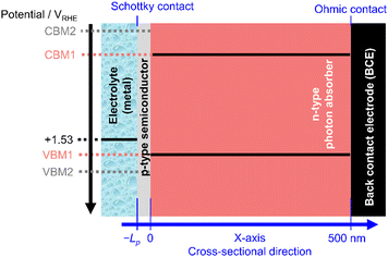
A schematic of the p–n heterojunction applied in this study is shown in Fig. 1. It is composed of a p-type semiconductor modification layer and an n-type photon absorber. The thickness of the p-type modification layer and the n-type photon absorber are Lp (variable) and 500 nm, respectively. The interface of the modification layer and electrolyte is assumed to be Schottky contact, whereas the interface of the photon absorber and metal back contact electrode (BCE) is set as the Ohmic contact.
Incident light is introduced from the electrolyte and absorbed in only the n-type photon absorber. The parasitic light absorption in the modification layer is ignored. According to the Lambert–Beer law, the following equation determines the charge generation rate:
| Gn(x) = Gp(x) = P0α exp(−αx) | (7) |
In this model, Shockley–Read–Hall (SRH) recombination that takes place via defect levels in the band gap was assumed to occur in only the photon absorber. The defect level is assumed to be located in the middle of the band gap. The recombination rate is expressed by the following equations:
 | (8) |
 | (9) |
In the simulation, the electrolyte was assumed to be metallic with a constant Fermi level. Considering the common overpotential during the OER (around 0.3 V at 10 mA cm−2),18 its Fermi level was tentatively set to 1.53 V vs. reversible hydrogen electrode (RHE). We believe that the assumption of the constant overpotential is reasonable because our current density range studied was below 10 mA cm−2 and because Tafel slopes of these catalysts are often reported to be 40–80 mV dec−1,18 which is not huge in our comparisons.
At this Schottky contact between the metal and p-type semiconductor, the electron and hole currents are determined by the carriers that overcome this barrier due to their thermal energy according to Fermi–Dirac distribution (i.e., thermionic emission current). The following equations determine the current flowing through the Schottky contact:
 | (10) |
 | (11) |
| J = Jp + Jn | (12) |
| Jp = qνp(p − p0) | (13) |
| Jn = −qνn(n−n0) | (14) |
From the bulk neutral region toward the junction, a narrow transition region appears. This region is called the space-charge region or, in some cases, the depletion region to be more specific, where electrons diffuse across the interface to combine with holes. The built-in potential, Vbi, represents the total of the electrostatic potential difference between the p- and n-type neutral regions at thermal equilibrium, where ψn and |ψp| are the electrostatic potential of the n- and p-type neutral region, respectively. To estimate xp and xn, the width of the depletion region in the p- and n-type regions respectively, the following equations were considered:
| Vbi = ψn + |ψp| | (15) |
 | (16) |
 | (17) |
 | (18) |
Tables 1 and 2 show the parameters of n-type Ta3N5 and those of the p-type modification layer, respectively. The varied parameters are highlighted in bold. Physical constants are shown in Table 3. In this study, we defined the onset potential as the point where the current density reaches 0.05 mA cm−2. Semi-log JV curves which were taken from Fig. 5a, as an example, are shown in Fig. S1 (ESI†). Although the onset potential may shift ca. 100 mV when the defined current density is changed by one order of magnitude below 0.1 mA cm−2, these curves are parallel, which means that the trend in the parametric study should be independent to the definition of the onset potential (below 0.1 mA cm−2).
| Symbol | Value | Unit | Description |
|---|---|---|---|
| CBM1 | −0.34 | V versus RHE (VRHE) | Conduction band minimum |
| VBM1 | +1.76 | V versus RHE (VRHE) | Valence band maximum |
| ε r | 17 | — | Relative permittivity |
| E g | 2.1 | eV | Band gap |
| c | 4.1 | eV | Electron affinity |
| N v | 1 × 10²⁰ | cm−3 | Effective density of states in VB |
| N c | 1 × 10²⁰ | cm−3 | Effective density of states in CB |
| μ n | 2 | cm2 V−1 s−1 | Electron mobility |
| μ p | 0.2 | cm2 V−1 s−1 | Hole mobility |
| N d | 1 × 10 19 | cm −3 | Donor density |
| τ n | 2 × 10⁻⁹ | s | Electron lifetime |
| τ p | 2 × 10⁻⁹ | s | Hole lifetime |
| P 0 | 9 × 10²⁰ | m−2 s−1 | Photon flux |
| α | 6 × 10⁶ | m−1 | Absorption coefficient |
| Symbol | Value | Unit | Description |
|---|---|---|---|
| L p | 25 | nm | Thickness of the modification layer |
| CBM2 | −1.14 | V versus RHE (VRHE) | Conduction band minimum |
| VBM2 | +2.26 | V versus RHE (VRHE) | Valence band maximum |
| ε r2 | 17 | – | Relative permittivity |
| E g2 | 3.4 | eV | Band gap |
| c 2 | 3.3 | eV | Electron affinity |
| N v | 1 × 10²⁰ | cm−3 | Effective density of states in VB |
| N c | 1 × 10²⁰ | cm−3 | Effective density of states in CB |
| μ n2 | 2 | cm2 V−1 s−1 | Electron mobility |
| μ p2 | 0.2 | cm2 V−1 s−1 | Hole mobility |
| N a | 1 × 10 19 | cm −3 | Acceptor density |
| Symbol | Value | Unit | Description |
|---|---|---|---|
| h | 6.62 × 10⁻³⁴ | J s | Planck constant |
| k B | 1.3806 × 10⁻²³ | J K−1 | Boltzmann constant |
| q | 1.602 × 10⁻¹⁹ | C | Elementary charge |
| μ 0 | 9.1094 × 10⁻³¹ | kg | Electron mass |
| μ n | 1.9 | Effective mass ratio of electron | |
| m p | 3.4 | Effective mass ratio of hole | |
| T | 298 | K | Temperature in model |
Results and discussion
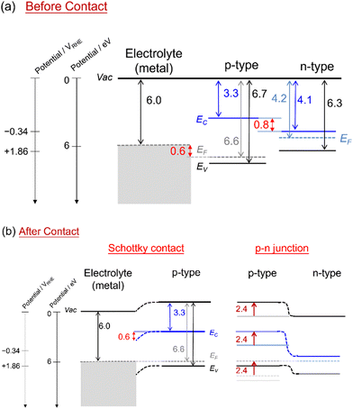
Fig. 2a shows the energy levels of separated layers, the electrolyte, the p-type modification layer, and the n-type photon absorber. The parameters are Na = 1 × 1019 cm−3, c = 3.3 eV, VBM2 = 2.26 VRHE, and Eg2 = 3.4 eV in the p-type layer, and Nd = 1 × 1019 cm−3, c = 4.1 eV, VBM2 = 1.76 VRHE, and Eg = 2.1 eV in the n-type layer. After they make contact with each other (Fig. 2b), due to the difference in the Fermi-level in the contacting layers, the free electrons and holes will be transferred across two materials to recombine. This process results in the formation of the depletion region and the electric field at the interface due to the remaining donor and acceptor ions until it reaches an equilibrium where the Fermi-level attains to the same level. Downward and upward band bending from the right-side semiconductor appear at the Schottky interface and p–n junction, respectively. The bending value depends on the difference between the valence band of the metal and the Fermi level in the p-type layer, which is 0.6 VRHE, as well as the difference from the n-type to the p-type layer, which is 2.4 VRHE in this example. Based on the predicted opposite bending, we performed a series of simulations to investigate the photoelectrochemical characteristics in the presence of the Schottky contact and the p–n junction.Effects of the valence band position in the p-type modification layer
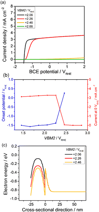
The valence band position in the p-type modification layer is expected to play an important role of guiding the holes from the bulk semiconductor to the electrolyte. The valence band position was varied to investigate the resulting current-potential curves and the band diagrams. The physical parameters of the n-type photon absorber were set as shown in Table 1. The valence band maximum of the p-type semiconducting modification layer, VBM2, was varied from +1.46 to +2.86 VRHE, and the other parameters were set constant, as shown in Table 2.In Fig. 3a, the VBM2 is varied from +2.06 to +2.46 VRHE. The current-potential curve changes significantly in this range, which can be explained by the band diagrams. Fig. 3b summarizes the photoanodic performance in response to VBM2. When the value of VBM2 went beyond +2.46, a significant transition of the onset potential was observed. The valence band diagrams are shown in Fig. 3c. Obviously, both the Schottky contact and p–n junction contribute to the present heterojunction. The upward bending from the bulk semiconductor to the interface developed by the p–n junction can effectively suppress the excited carriers that recombine in the photon absorber. A V-shape band structure also appears at the heterointerface between the p-type and n-type layers. Its depth strongly depends on VBM2.
The huge gap (>0.6 eV) might have blocked the photogenerated holes from transferring from the photon absorber to the modification layer at the highest VBM2 of 2.46 VRHE. The gap was smaller when reducing VBM2, which allowed accumulated holes to pass through the interface. Overall, the relatively low VBM2 (below 2.2 VRHE) is preferable for achieving unbiased water splitting.
Remarkably, although VBM2 is more positive than VBM1 (1.76 VRHE), a clear photodiode characteristic was still obtained. To develop the present p–n junction with the OER catalyst layer, for example, the valence band position of NiOx is reported to be 1.0 VRHE,65 and Sun et al. successfully produced oxygen using p-type NiOx as an OER catalyst on an n-Si photoanode.66 In the present study, VBM2 was varied while CBM2 was maintained which means that the band gap in the p-type layer changes. The band gap in the p-type layer is 3.2–3.8 eV while that in the n-type layer is 2.1 eV, which suggests that parasitic light absorption by the modification layer can be ignored. However, a trade-off effect should be considered when the band gap of the p-type layer is comparable to that in the n-type layer.
Impact of the acceptor density in the p-type modification layer
The effect of Na on the PEC performance was investigated. The donor density was fixed at 1 × 1019 cm−3, as shown in Table 1, and Na was varied from 1 × 10¹⁷ to 1 × 1019 cm−3. The simulated current-potential curves are shown in Fig. 4a, and the extracted current density at 0 VRHE and the onset potential are shown in Fig. 4d. The current density remains almost constant, and the onset potential does not vary dramatically when the Na concentration is below approximately 3 × 1018 cm−3. In this range, the calculated depletion depth from eqn (16) and (17) in the p-type layer is much thicker than the setting value (25 nm). The result can be explained by the green curve in Fig. 4d and e, where the depletion in the p-type layer cannot form completely. This leads to a recombination loss mechanism, as shown by the high hole density in the n-type layer near the interface.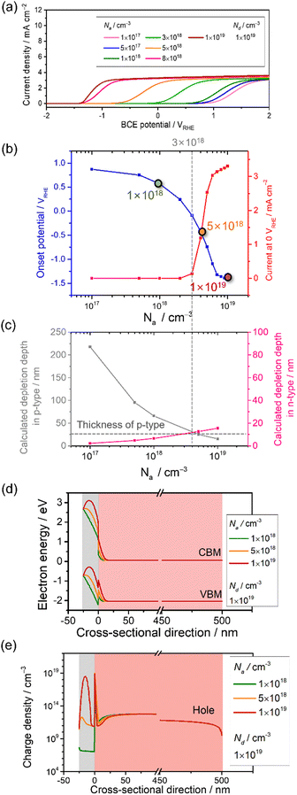 | ||
| Fig. 4 Current-potential of a p–n junction photoanode with varied acceptor density in the p-type modification layer, Na, from 1 × 1017 cm−3 to 1 × 1019 cm−3. Nd is maintained at 1 × 1019 cm−3. (b) Extracted onset potential and current density at 0 VRHE with respect to Na. (c) The depletion depth in the p-type region (grey) and n-type region (pink) with varied Na estimated from eqn (16) and (17). (d) Energy band diagram and (e) charge density with Na varied from 1 × 1018 cm−3 to 1 × 1019 cm−3 at 0 VRHE. | ||
The current density at 0 VRHE increases sharply at 3 × 1018 cm−3, and the onset potential is negatively shifted by approximately 2.5 V vs. RHE when increasing Na. Undeniably, a depletion region in the p-type modification layer is formed by both p–n junction and Schottky contact. Although the opposite bending from the Schottky contact appears, increasing Na reduces the depletion depth in the p-type layer coming from the p–n interface (Fig. 4c and d). In this critical section, the tendency starts to drastically change.
Lastly, the thickness of the depletion region in the p-type modification layer developed by the p–n junction becomes thin compared to the modification layer (25 nm). Hence, when Na reaches 1 × 1019 cm−3, the fully developed p–n junction forms a stronger electric field that drives the holes toward the electrolyte. The density distribution of minority holes along the cross-sectional direction (Fig. 4e) indicates that the hole density in the n-type layer near the interface decreases when increasing Na, which means that the recombination loss mechanism is weakened.
V-shape traps are present at the interface between the p- and n-type layers due to the heterojunction (Fig. 4d), but their contribution seems to be minor as long as VBM2 is negative enough, as discussed in Section 3.1. OER catalyst modification layers are often deposited on semiconductors by dry or wet processes. Wet processes such as electrodeposition and spin coating naturally result in high doping concentrations. Considering the present results, wet processes seem to be preferable to dry vacuum processes, which result in high-quality films.
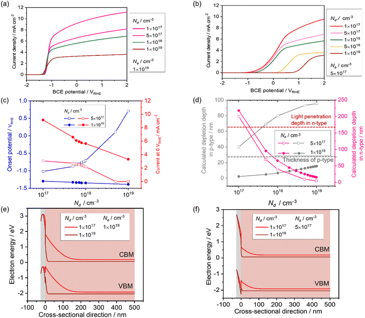
Influence of donor density in the n-type photon absorber
The effect of the donor density in the photon absorber, Nd, was next investigated with different values of Na to see the influence on the current-potential curves. The other parameters in the p-type modification layer were maintained as shown in Table 2. Firstly, Nd was varied from 1 × 10¹⁷ to 1 × 1019 cm−3, and Na was fixed at 1 × 1019 cm−3. As shown in Fig. 5a, the current density at 0 VRHE decreases from 9 to 3 mA cm−2 when increasing Nd. Secondly, with relatively low Na (5 × 1017 cm−3), the current density decreases from 3 to 0 mA cm−2 (Fig. 5b). Fig. 5c shows the extracted onset potential values and the current densities at 0 VRHE from the current–potential curves. When the p–n junction is fully developed in the modification layer in the range of Nd variation (Fig. 5d), the onset potential remained constant. When Na and Nd are at comparable levels, the onset potential shifts when changing Nd because the depletion depth in the p-type region also varies with Nd (Fig. 5e).Considering the light penetration depth of 170 nm, a relatively low donor density is preferable because the width of the depletion region in the n-type photon absorber is thick enough to cover the light penetration depth (Fig. 5e). Therefore, excited charge carriers can be effectively migrated by the electric field in the depletion layer. Enlargement of the depletion layer in the photon absorber can also be found in the simulated band diagram (Fig. 5d and f). Therefore, for an n-type photon absorber, high quality with a low dopant concentration is required since the donor density in the photon absorber strongly affects the attainable photocurrent.
Donor density determines the resistivity in the bulk n-type region and the resultant ohmic voltage loss. Using the parameters in Table 1 and the donor density of 1 × 1017 cm−3, the resistance and the ohmic voltage loss were estimated to be 1.6 mΩ and 1.6 × 10⁻² mV, respectively, at 10 mA cm−2 with an area of 1 cm2 and a thickness of 500 nm. This ohmic voltage loss is negligible in our JV curves, which indicates that the conductivity and the thickness in the bulk n-type region do not play a major role in our simulation.
Consideration of the modification layer thickness with respect to the depletion depth
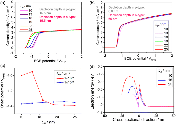
The thickness of the p-type modification layer was varied from 10 to 25 nm with fixed Na (1 × 1019 cm−3). Nd is 1 × 1019 cm−3 and 1 × 1018 cm−3 in Fig. 6a and b, respectively. As Fig. 6c shows, the onset potential is negatively shifted when the thickness increases. When the donor density is reduced to 1 × 1018 cm−3, a constant onset potential was obtained because the thickness of the depletion depth in the p-type region (6.6 nm) is less than the simulated thickness range, which results in a fully developed p–n junction (Fig. 6d). Therefore, the thickness of the modification layer should be carefully designed to cover the depletion depth, which is determined by the dopant densities. A thick modification layer would result in parasitic light absorption, which is not considered in the present study. The trade-off highlights the severe restriction on the catalyst modification, which is unique compared to p–n photovoltaic or buried p–n junction photoelectrodes.Comparison between the p–n junction and n–n junction
The tendencies on the varied parameters were compared between the p–n junction and an n–n junction,58 as shown in Fig. 7. The effects of the modification layer thickness in these two junctions are opposite. For the n–n heterojunction, favorable upward bending was predicted at the heterointerface in the thinnest one (10 nm), while unfavorable bending appeared at the n–n interface with a thicker layer. The critical distinction from the n–n junction is the formation of a depletion layer in the p–n junction, which results in the development of an electric field. Therefore, the p-type modification layer needs to be thick enough to fully develop the depletion layer.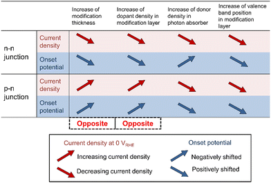 | ||
| Fig. 7 Comparison of the current density at 0 VRHE and onset potential between the n–n junction58 and p–n junction. | ||
The effects of the dopant density in the modification layer in these two situations are opposite as well. From the charge density distribution in the n–n heterojunction, an increase in the hole (minority carrier) concentration was observed in the n-type photon absorber near the interface with increasing donor density in the modification layer, which enhanced the electron-hole recombination. The fully developed p–n junction can contribute a stronger electric field to drive the holes towards the electrolyte. Increasing Na can reduce the depletion depth in the p-type layer at the p–n interface. Thus, a decrease in the hole concentration can be observed in the n-type photon absorber with increasing acceptor density of the modification layer, leading to the suppression of the recombination.
A lower donor density in the photon absorber is obviously preferable to improve the attainable photocurrent because the thickness of the depletion region in the photon absorber is increased to cover the light penetration depth. This results in the effective migration of the excited carriers due to the electric field. However, the effect of donor density in the photon absorber shows a trade-off relationship between the onset potential and the current density in the n–n heterojunction, indicating that the donor density needs to be carefully optimized for the target operation. A lower doner density is preferable in the p–n heterojunction because it helps the formation of the fully developed p–n junction in the thin layer. Lastly, the effects of valence band position in the modification layer have the same tendency. Relatively low VBM2 is preferable because the favorable band bending appears to improve the performance.
The current ideal modeling of the semiconductor junction predicts the p-type modification layer to be a better candidate rather than n-type modification for enhancing the photoelectrocatalytic performance because of the lower onset potential of the p–n junction. Theoretically, the built-in electric field in a p–n junction is stronger than the n–n junction, which is consistent with this result. These studies should be able to provide a quantitative guideline for establishing thin layer modification of the photoelectrode.
Conclusions
In this study, we used classical semiconductor theory to demonstrate a series of simulations to enhance the performance of an n-type photoanode covered with a thin p-type modification layer. Several pivotal parameters were analyzed to provide a guideline to achieve a higher photocurrent density without any bias, including the valence band position, dopant densities in both the p-type modification layer and n-type photon absorber, and the thickness of the modification layer. Also, we investigated the difference between the p–n junction and an n–n heterojunction. To design an ideal p–n heterojunction, the depletion depths in the p-type modification layer and n-type photon absorber must carefully be tuned with respect to the thickness of the modification layer and the light penetration depth by controlling their dopant densities. Furthermore, VBM2 should be below 0.44 VRHE from the valence band position in the n-type absorber. Undeniably, more conditions should be considered for the photoanode design model since the model was applied using the classical theory, and we neglected some realistic potential-dependent reaction kinetics, parasitic light absorption, and the other factors. However, this study could still provide an idea of how to improve a photoanode covered with a thin layer of p-type OER electrocatalysts.Author contributions
Conceptualization, F. K. and K. T.; methodology, H. H. and K. O.; investigation, H. H., F. K. and K. O.; writing – original draft, H. H.; writing – review & editing, H. H., K. O., F. K., and K. T.; supervision, K. T.; funding acquisition, K. T.Conflicts of interest
There are no conflicts to declare.Acknowledgements
The authors thank Prof. Akira Nakayama of the University of Tokyo for supplying the COMSOL software and a calculation server. This work was supported by the Mohammed bin Salman Center for Future Science and Technology for Saudi-Japan Vision 2030 at the University of Tokyo (MbSC2030).References
- J. Brillet, M. Comuz, F. LeFormal, J. H. Yum, M. Grätzel and K. Sivula, J. Mater. Res., 2010, 25, 17–24 CrossRef CAS.
- Q. Wang, T. Hisatomi, Y. Suzuki, Z. Pan, J. Seo, M. Katayama, T. Minegishi, H. Nishiyama, T. Takata, K. Seki, A. Kudo, T. Yamada and K. Domen, J. Am. Chem. Soc., 2017, 139, 1675–1683 CrossRef CAS.
- S. Chen, T. Takata and K. Domen, Nat. Rev. Mater, 2017, 2, 17050 CrossRef CAS.
- T. Hisatomi, J. Kubota and K. Domen, Chem. Soc. Rev., 2014, 43, 7520–7535 RSC.
- X. Chen, S. Shen, L. Guo and S. S. Mao, Chem. Rev., 2010, 110, 6503–6570 CrossRef CAS PubMed.
- M. G. Walter, E. L. Warren, J. R. McKone, S. W. Boettcher, Q. Mi, E. A. Santori and N. S. Lewis, Chem. Rev., 2010, 110, 6446–6473 CrossRef CAS PubMed.
- L. Finegold and J. L. Cude, Nature, 1972, 238, 38–40 CrossRef CAS PubMed.
- S. S. Mao, S. Shen and L. Guo, Prog. Nat. Sci. Mater. Int, 2012, 22, 522–534 CrossRef.
- W. H. Cheng, M. H. Richter, M. M. May, J. Ohlmann, D. Lackner, F. Dimroth, T. Hannappel, H. A. Atwater and H. J. Lewerenz, ACS Energy Lett, 2018, 3, 1795–1800 CrossRef CAS.
- Y. Pihosh, I. Turkevych, K. Mawatari, J. Uemura, Y. Kazoe, S. Kosar, K. Makita, T. Sugaya, T. Matsui, D. Fujita, M. Tosa, M. Kondo and T. Kitamori, Sci. Rep, 2015, 5, 11141 CrossRef.
- B. A. Pinaud, J. D. Benck, L. C. Seitz, A. J. Forman, Z. Chen, T. G. Deutsch, B. D. James, K. N. Baum, G. N. Baum, S. Ardo, H. Wang, E. Miller and T. F. Jaramillo, Energy Environ. Sci., 2013, 6, 1983–2002 RSC.
- T. Higashi, H. Nishiyama, Y. Suzuki, Y. Sasaki, T. Hisatomi, M. Katayama, T. Minegishi, K. Seki, T. Yamada and K. Domen, Angew. Chem., Int. Ed., 2019, 58, 2300–2304 CrossRef CAS PubMed.
- S. Hu, C. Xiang, S. Haussener, A. D. Berger and N. S. Lewis, Energy Environ. Sci., 2013, 6, 2984–2993 RSC.
- K. T. Fountaine, H. J. Lewerenz and H. A. Atwater, Nat. Commun., 2016, 7, 13706 CrossRef CAS.
- Y. Pihosh, T. Minegishi, V. Nandal, T. Higashi, M. Katayama, T. Yamada, Y. Sasaki, K. Seki, Y. Suzuki, M. Nakabayashi, M. Sugiyama and K. Domen, Energy Environ. Sci., 2020, 13, 1519–1530 RSC.
- W. Smith, A. Wolcott, R. C. Fitzmorris, J. Z. Zhang and Y. Zhao, J. Mater. Chem., 2011, 21, 10792–10800 RSC.
- Y. Pihosh, V. Nandal, T. Minegishi, M. Katayama, T. Yamada, K. Seki, M. Sugiyama and K. Domen, ACS Energy Lett, 2020, 5, 2492–2497 CrossRef CAS.
- N. T. Suen, S. F. Hung, Q. Quan, N. Zhang, Y. J. Xu and H. M. Chen, Chem. Soc. Rev., 2017, 46, 337–365 RSC.
- T. J. Mills, F. Lin and S. W. Boettcher, Phys. Rev. Lett., 2014, 112, 148304 CrossRef PubMed.
- M. R. Nellist, F. A. L. Laskowski, F. Lin, T. J. Mills and S. W. Boettcher, Acc. Chem. Res., 2016, 49, 733–740 CrossRef CAS PubMed.
- M. S. Burke, M. G. Kast, L. Trotochaud, A. M. Smith and S. W. Boettcher, J. Am. Chem. Soc., 2015, 137, 3638–3648 CrossRef CAS PubMed.
- D. Maity, K. Karmakar and K. Mandal, J. Alloys Compd., 2019, 791, 739–746 CrossRef CAS.
- M. S. Burke, S. Zou, L. J. Enman, J. E. Kellon, C. A. Gabor, E. Pledger and S. W. Boettcher, J. Phys. Chem. Lett., 2015, 6, 3737–3742 CrossRef CAS PubMed.
- S. Xie, T. Zhai, Y. Zhu, W. Li, R. Qiu, Y. Tong and X. Lu, Int. J. Hydrogen Energy, 2014, 39, 4820–4827 CrossRef CAS.
- S. S. Yi, B. R. Wulan, J. M. Yan and Q. Jiang, Adv. Funct. Mater., 2019, 29, 1801902 CrossRef.
- F. A. L. Laskowski, M. R. Nellist, R. Venkatkarthick and S. W. Boettcher, Energy Environ. Sci., 2017, 10, 570–579 RSC.
- F. A. L. Laskowski, S. Z. Oener, M. R. Nellist, A. M. Gordon, D. C. Bain, J. L. Fehrs and S. W. Boettcher, Nat. Mater., 2020, 19, 69–76 CrossRef CAS PubMed.
- A. T. Garcia-Esparza and K. Takanabe, J. Mater. Chem. A, 2016, 4, 2894–2908 RSC.
- Y. Kawase, T. Higashi, M. Katayama, K. Domen and K. Takanabe, ACS Appl. Mater. Interfaces, 2021, 13, 16317–16325 CrossRef CAS.
- S. S. Gujral, A. N. Simonov, M. Higashi, X. Y. Fang, R. Abe and L. Spiccia, ACS Catal., 2016, 6, 3404–3417 CrossRef CAS.
- S. Li, C. Wang, M. Cai, F. Yang, Y. Liu, J. Chen, P. Zhang, X. Li and X. Chen, Chem. Eng. J., 2022, 428, 131158 CrossRef CAS.
- Z. Wang, J. Hou, S. Jiao, K. Huang and H. Zhu, J. Mater. Chem., 2012, 22, 21972–21978 RSC.
- H. Jiang, W. Zhang, S. Zang and W. Zhang, Int. J. Hydrogen Energy, 2019, 44, 24218–24227 CrossRef CAS.
- L. Pei, T. Li, Y. Yuan, T. Yang, J. Zhong, Z. Ji, S. Yan and Z. Zou, Chem. Commun., 2019, 55, 11754–11757 RSC.
- M. Hara, G. Hitoki, T. Takata, J. N. Kondo, H. Kobayashi and K. Domen, Catal. Today, 2003, 78, 555–560 CrossRef CAS.
- S. Wang, Z. Li, Y. Guan, L. Lu, Z. Shi, P. Weng, S. Yan and Z. Zou, Appl. Catal. B Environ., 2019, 245, 220–226 CrossRef CAS.
- H. Jiang, L. Feng, S. Zhu, X. Li and S. Zang, Int. J. Hydrogen Energy, 2021, 46, 39855–39867 CrossRef CAS.
- H. Jiang, X. Li, S. Zang and W. Zhang, J. Alloys Compd., 2021, 854, 155328 CrossRef CAS.
- A. Yamakata, M. Kawaguchi, N. Nishimura, T. Minegishi, J. Kubota and K. Domen, J. Phys. Chem. C, 2014, 118, 23897–23906 CrossRef CAS.
- X. Lu, A. Bandara, M. Katayama, A. Yamakata, J. Kubota and K. Domen, J. Phys. Chem. C, 2011, 115, 23902–23907 CrossRef CAS.
- A. Ishikawa, T. Takata, J. N. Kondo, M. Hara and K. Domen, J. Phys. Chem. B, 2004, 108, 11049–11053 CrossRef CAS.
- C. T. Ho, K. BinLow, R. F. Klie, K. Maeda, K. Domen, R. J. Meyer and P. T. Snee, J. Phys. Chem. C, 2011, 115, 647–652 CrossRef CAS.
- D. Choi and P. N. Kumta, J. Am. Ceram. Soc., 2007, 90, 3113–3120 CrossRef CAS.
- V. Nandal, Y. Pihosh, T. Higashi, T. Minegishi, T. Yamada, K. Seki, M. Sugiyama and K. Domen, Energy Environ. Sci., 2021, 14, 4038–4047 RSC.
- G. Hitoki, A. Ishikawa, T. Takata, J. N. Kondo, M. Hara and K. Domen, Chem. Lett., 2002, 736–737 CrossRef CAS.
- M. Li, W. Luo, D. Cao, X. Zhao, Z. Li, T. Yu and Z. Zou, Angew. Chem., Int. Ed., 2013, 52, 11016–11020 CrossRef CAS.
- J. Fu and S. E. Skrabalak, J. Mater. Chem. A, 2016, 4, 8451–8457 RSC.
- Y. Jiang, P. Liu, Y. C. Chen, Z. Zhou, H. Yang, Y. Hong, F. Li, L. Ni, Y. Yan and D. H. Gregory, Appl. Surf. Sci., 2017, 391, 392–403 CrossRef CAS.
- R. Gao, S. Zhou, M. Chen and L. Wu, J. Mater. Chem., 2011, 21, 17087–17090 RSC.
- S. Chen, Y. Qi, Q. Ding, Z. Li, J. Cui, F. Zhang and C. Li, J. Catal., 2016, 339, 77–83 CrossRef CAS.
- S. Grigorescu, B. Bärhausen, L. Wang, A. Mazare, J. E. Yoo, R. Hahn and P. Schmuki, Electrochem. commun., 2015, 51, 85–88 CrossRef CAS.
- X. Zhan, Z. Fang, B. Li, H. Zhang, L. Xu, H. Hou and W. Yang, J. Mater. Chem. A, 2021, 9, 27084–27094 RSC.
- H. Wang, L. Zhang, Z. Chen, J. Hu, S. Li, Z. Wang, J. Liu and X. Wang, Chem. Soc. Rev., 2014, 43, 5234–5244 RSC.
- H. Li, Y. Zhou, W. Tu, J. Ye and Z. Zou, Adv. Funct. Mater., 2015, 25, 998–1013 CrossRef CAS.
- W. Zhang, H. Jiang, W. Zhang and S. Zang, RSC Adv., 2020, 10, 29424–29431 RSC.
- W. P. Hsu, M. Mishra, W. S. Liu, C. Y. Su and T. P. Perng, Appl. Catal. B Environ., 2017, 201, 511–517 CrossRef CAS.
- P. Zhang, T. Wang and J. Gong, Chem. Commun., 2016, 52, 8806–8809 RSC.
- K. Hatagami, F. Kishimoto, Y. Kawase, T. Higashi, V. Nandal, K. Seki and K. Takanabe, Energy Technol., 2022, 10, 2100570 CrossRef CAS.
- S. Li, S. Hu, K. Xu, W. Jiang, Y. Liu, Z. Leng and J. Liu, J. Colloid Interface Sci., 2017, 504, 561–569 CrossRef CAS PubMed.
- M. Liao, J. Feng, W. Luo, Z. Wang, J. Zhang, Z. Li, T. Yu and Z. Zou, Adv. Funct. Mater., 2012, 22, 3066–3074 CrossRef CAS.
- A. Ziani, E. Nurlaela, D. S. Dhawale, D. A. Silva, E. Alarousu, O. F. Mohammed and K. Takanabe, Phys. Chem. Chem. Phys., 2015, 17, 2670–2677 RSC.
- E. Nurlaela, S. Ould-Chikh, M. Harb, S. DelGobbo, M. Aouine, E. Puzenat, P. Sautet, K. Domen, J. M. Basset and K. Takanabe, Chem. Mater., 2014, 26, 4812–4825 CrossRef CAS.
- H. Hajibabaei, O. Zandi and T. W. Hamann, Chem. Sci., 2016, 7, 6760–6767 RSC.
- E. Nurlaela, Y. Sasaki, M. Nakabayashi, N. Shibata, T. Yamada and K. Domen, J. Mater. Chem. A, 2018, 6, 15265–15273 RSC.
- S. Bai, M. Cao, Y. Jin, X. Dai, X. Liang, Z. Ye, M. Li, J. Cheng, X. Xiao, Z. Wu, Z. Xia, B. Sun, E. Wang, Y. Mo, F. Gao and F. Zhang, Adv. Energy Mater., 2014, 4, 1301460 CrossRef.
- K. Sun, N. Park, Z. Sun, J. Zhou, J. Wang, X. Pang, S. Shen, S. Y. Noh, Y. Jing, S. Jin, P. K. L. Yu and D. Wang, Energy Environ. Sci., 2012, 5, 7872–7877 RSC.
Footnote |
| † Electronic supplementary information (ESI) available. See DOI: https://doi.org/10.1039/d2ma00947a |
| This journal is © The Royal Society of Chemistry 2022 |

