
 Open Access Article
 This Open Access Article is licensed under a Creative Commons Attribution-Non Commercial 3.0 Unported Licence
Unusual electronic transport in (1 − x)Cu2Se–(x)CuInSe2 hierarchical composites†
Yixuan
Chen
 ab,
Yinying
Zhang
c,
Ruiming
Lu
a,
Trevor P.
Bailey
c,
Ctirad
Uher
c and
Pierre F. P.
Poudeu
*ab
ab,
Yinying
Zhang
c,
Ruiming
Lu
a,
Trevor P.
Bailey
c,
Ctirad
Uher
c and
Pierre F. P.
Poudeu
*ab
aLaboratory for Emerging Energy and Electronic Materials (LE3M), Department of Materials Science and Engineering, University of Michigan, Ann Arbor, MI 48109, USA. E-mail: ppoudeup@umich.edu; Fax: +1-734-763-4788
bDepartment of Chemical Engineering, University of Michigan, Ann Arbor, MI 48109, USA
cDepartment of Physics, University of Michigan, Ann Arbor, MI 48109, USA
First published on 26th August 2022
Abstract
The ability to control the relative density of electronic point defects as well as their energy distribution in semiconductors could afford a systematic modulation of their electronic, optical, and optoelectronic properties. Using a model binary hybrid system Cu2Se–CuInSe2, we have investigated the correlation between phase composition, microstructure, and electronic transport behavior in the synthesized composites. We found that both Cu2Se and CuInSe2 phases coexist at multiple length scales, ranging from sub-ten nanometer to several micrometers, leading to the formation of a hybrid hierarchical microstructure. Astonishingly, the electronic phase diagram of the (1 − x)Cu2Se–(x)CuInSe2 (15% ≤ x ≤ 100%) hierarchical composites remarkably deviates from the trend normally expected for composites between a heavily doped semiconductor (Cu2Se) and a poorly conducting phase (CuInSe2). A sudden 3-fold increase in the electrical conductivity and carrier concentration along with a marginal increase in the carrier mobility is observed for composites at the vicinity of equimolar composition (48% ≤ x ≤ 52%). The carrier concentration increases from ∼1.5 × 1020 cm−3 for the composites with x ≤ 45% to 5.0 × 1020 cm−3 for x = 50%, and remains constant at 4.5 × 1020 cm−3 with x value in the range of 52% < x ≤ 90%, then quickly drops to 8 × 1018 cm−3 for pristine CuInSe2 phase (x = 100%). The atypical electronic behavior was rationalized in the light of the formation of an inter-band (IB) within the band gap, which arises from the hybridization of native electronic point defects from both Cu2Se and CuInSe2 phases in the resulting hierarchical composites. The result points to a new strategy to modulate the electronic structure of semiconductor composites to maximize interaction and coupling between two fundamentally contrasting properties enabling access to electronic hybrid systems with potential applications as interactive and stimuli-responsive multifunctional materials.
1. Introduction
Semiconductor materials and devices have been powering the information technologies since the invention of transistor in 1947,1 and continue to bring about technological innovations, which deeply revolutionize our lives today. An important step in designing a semiconductor with a unique functionality, such as electrical conductivity, light absorption and emittance, magnetism, etc.2–5 relies on the understanding and manipulation of the type, density, as well as the energy distribution of electronic point defects within the crystal structures. Point defects are crucial in dictating the electronic performance of semiconductors as they afford the opportunity to control more fundamental parameters, namely the carrier concentration and mobility, that significantly influence macroscopic properties, such as the magnetism,6 piezoelectricity,7 superconductivity,8 thermoelectricity,9,10etc.Point defects engineering via doping the host material using heterovalent atoms or/and through deliberate off-stoichiometry,11 remains the most popular approach to tune the concentration of free carriers in semiconductors. The change generated by doping is usually monotonic, especially when the dopant only generates one type of electronic defect. For example, the number of free electrons (holes) would increase with increasing donor (acceptor) dopant concentration until a bottleneck is reached.12,13 This feature has given researchers an intuitive approach to improve the functionalities of semiconductors, however, it can usually only optimize the intrinsic single functionality.
Unfortunately, this traditional method of tuning dopant concentration may be insufficient for the development of more intelligent semiconductors for next generation high-performance electronic devices, such as stimuli responsive multifunctional semiconductors, which can adapt to varying environments or allow remote control over one functionality by another. In pursuit of such advanced semiconductors, efforts have been made to incorporate dopants that can add new functionalities to the host material. For example, Ni2+ was integrated into ZnSe, CdZnS and CuInS2 nanocrystals to enable above room-temperature ferromagnetism which coexisted with the tunable optical emission originating from the nanocrystals.14 Currently, many efforts to design multifunctional semiconductors have been focused on doping transition metals in quantum dots hosts,15 taking advantage of their quantum confinement effects. Despite many advantages of quantum dots (chemical and physical tunability, high quantum efficiency), there still exist numerous challenges for this nanoscale semiconductor, particularly its metastability and synthesis difficulties.16 In addition, the coupling between the coexisting functionalities in traditional multifunctional materials remains weak. Therefore, exploring new ways to create strongly interacting multifunctionalities in semiconductors is of paramount importance if one wants to develop high-performance stimuli-responsive semiconductors for next generation electronic devices.
Here, we introduce an elegant approach to multifunctional semiconducting materials featuring a strong interaction between two fundamentally contrasting functionalities. Our strategy consists of the structural integration, at multiple length scales (from nano- to micron-scale), of two phases with dissimilar but related structures and chemistries, each of which possesses a single functionality, into a hybrid composite hierarchical structure. We anticipate that the unique intimate connectivity between structural fragments from both phases at multiscale can give rise to strong interaction between the coexisting functionalities, which could lead to new physical phenomena and stimuli-responsive behaviors.
To explore this concept, we have synthesized a series of hybrid (1 − x)Cu2Se/(x)CuInSe2 (15% ≤ x ≤ 100%) composites within which Cu2Se-rich and CuInSe2-rich domains with various size and shapes are intimately integrated at the micron as well as nanometer scale. The Cu2Se–CuInSe2 hybrid system provides a model platform for the investigation of how the hierarchical structure integration of two semiconductors with different band gaps and electrical conductivities modifies electronic transport in the resulting composites. Beyond the similarity in their chemical constituents, both Cu2Se and CuInSe2 are well studied technologically important materials. β-Cu2Se is a narrow band gap semiconductor that has attracted increasing attention for use as a promising thermoelectric material,17–23 whereas CuInSe2 is a wider band gap semiconductor with high absorption coefficient used as a solar absorber layer in solar cell devices.24,25 Moreover, a recent study on Cu2Se reported the electroresistance effect, induced by electric-field-driven crystalline orientation change.26 Therefore it is reasonable to expect that (1 − x)Cu2Se/(x)CuInSe2 composites would exhibit interactions with several external stimuli, such as light, temperature gradient and electric potential. In addition, the coexistence of native donor and acceptor point defects in both pristine Cu2Se and CuInSe2 phases makes this system particularly attractive for investigations of the change in the interaction between these defects upon varying the phase ratio between Cu2Se and CuInSe2. The systems provide the opportunity to probe the electronic band structure of various (1 − x)Cu2Se/(x)CuInSe2 composites. For instance, elucidating how the density and distribution of donor and acceptor point defects are altered in various composites could pave the way to a better understanding of the dynamics of electronic transport under various external stimuli such as temperature and illumination.
(1 − x)Cu2Se/(x)CuInSe2 composites with the desired hierarchical integration between Cu2Se-rich and CuInSe2-rich domains were fabricated through a single step solid-state transformation of a CuSe2 template following a reaction concept described by Olvera et al.17 The similarity in the lattice parameters (within the ab plane) of the cubic β-Cu2Se and the tetragonal CuInSe2 phases at the reaction temperature facilitates the formation of stable semi-coherent interfaces, which enables the creation of Cu2Se nano-domains within the CuInSe2 micron size domain ([Cu2Se]nano@[CuInSe2]micron) simultaneously with the formation of CuInSe2 nano domains within the Cu2Se micron size particle ([CuInSe2]nano@[Cu2Se]micron). With the unique microstructure, unexpected trend in electrical conductivity was revealed, with a sudden large increase near the equimolar compositions (48% ≤ x ≤ 52%). Investigation of carrier concentration and mobility on selected compositions not only explains the observed large increase in the electrical conductivity for equimolar compositions, but also indicates a significant alteration of the density and energy distribution of point defects in various composites and suggests a unique interaction between point defects for nearly equimolar compositions. The observed peculiar electronic behavior for equimolar (1 − x)Cu2Se/(x)CuInSe2 composites is rationalized within the context of an interband (IB) formation arising from the hybridization of shallow and deep acceptor states from both the Cu2Se and CuInSe2 phases. This work demonstrates that several unexpected stimuli-responsive semiconducting behaviors with potentially significant technological applications may emerge from hierarchical hybrid structures constructed between different semiconductors.
2. Experimental section
2.1. Sample preparation
High-purity Cu (99.5%, Alfa Aesar), Se (≥99.5%, Sigma-Aldrich) and In (99.99%, Alfa Aesar) powders were used for the material synthesis. The (1 − x)Cu2Se/(x)CuInSe2 composites were synthesized via a one-step solid-state reaction, following the chemical equation below:| CuSe2 + (y)In + 3(1 − y)Cu → (y)CuInSe2 + 2(1 − y)Cu2Se |
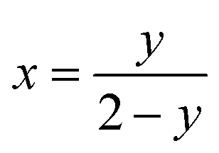
The mole fraction (x) of CuInSe2 reported for various (1 − x)Cu2Se/(x)CuInSe2 composites is calculated as:
The CuSe2 precursor was synthesized through a solid-state reaction of stoichiometrically mixed elemental Cu and Se powders. The mixed powder was flame-sealed into a quartz tube under dynamic vacuum (10−3 torr). The sealed tube was heated at 210 °C for 24 hours, followed by another heating at 320 °C for 36 hours. A second annealing of the resulting product at 270 °C for an additional 72 hours was necessary to obtain a single phase CuSe2 sample. To prepare (1 − x)Cu2Se/(x)CuInSe2 composites, the desired amount of In and Cu powders were thoroughly mixed with the CuSe2 precursor and sealed in a quartz tube under a residual pressure of 10−3 torr. The mixtures were reacted following a stepwise heating profile: 150 °C for 24 hours, 320 °C for 48 hours and 600 °C for 48 hours. This process enables the simultaneous conversion of CuSe2 into CuInSe2 and Cu2Se. The final product was pulverized into fine powder by hand-grinding. Then the powder was loaded into a graphite die and densified at 500 °C under vacuum using a uniaxial hot press with a pressure of 100 MPa. Two rectangular bar-shape specimens were cut out from the obtained high-density cylindrical bulk sample, one of which was used for electrical conductivity measurement, and another was used for the Hall measurement.
2.2. Characterization
Powder X-ray diffraction (PXRD) was conducted to determine the phase composition and crystal structure of both the as-synthesized powder and the densified samples. The Rigaku Smartlab X-ray diffractometer was operated at 40 kV and 44 mA with Cu Kα incident radiation (λ = 1.54059 Å), and a D/tex ultra 250 high-speed detector on the receiving side. Differential scanning calorimetry (DSC) was carried out on a Netzsch DSC 404 F1 Pegasus to investigate the evolution of the thermal behavior of Cu2Se and CuInSe2 phases in (1 − x)Cu2Se/(x)CuInSe2 composites upon varying the CuInSe2 phase fraction (x value). DSC data also helped to assess the thermal stability of the samples. The microstructure and phase distribution of the densified samples were evaluated by a JEOL JSM-7800FLV scanning electron microscope, which was operated under backscatter electron (BSE) detection mode. Chemical composition was also analyzed by the energy dispersive spectrum (EDS) mapping with the attached Oxford XMaxN 80 mm2 silicon-drift energy-dispersive X-ray spectrometer. Nano-scale phase integration was examined by a JEOL 3100R05 transmission electron microscope (TEM) with double Cs correction, operated at 300 kV. The electrical conductivity was measured with a ULVAC-RIKO ZEM-3 system by four-probe method from room temperature up to 773 K with low-pressure helium gas. Hall coefficient was obtained on a home-built instrument under ±0.5 T magnetic field.3. Results and discussion
3.1. Synthesis and microstructure
The approach utilized to synthesize the array of (1 − x)Cu2Se/(x)CuInSe2 composites is adapted from the versatile topochemical method previously developed in our group.17,27 This synthesis concept relies on the reductive solid-state transformation of a sacrificial template CuSe2, where Cu2+ and (Se2)2− are reduced to Cu+ and Se2− upon introduction of metallic copper and indium powders. Due to the compositional and structural similarities between CuSe2 and the targeted phases (Cu2Se and CuInSe2), a direct and simultaneous conversion from the CuSe2 precursor to the final products in a single step is expected, which minimizes the formation of undesirable impurities. To probe the comprehensive changes in the electronic transport properties, as well as the microstructure evolution, within various portions of the Cu2Se–CuInSe2 pseudo-binary system, a total number of 23 compositions were selected and prepared. They can be divided into four groups: (i) 15% ≤ x ≤ 30% (4 samples); (ii) 40% ≤ x ≤ 60% (7 samples); (iii) 65% ≤ x ≤ 90% (7 samples), and (iv) 92% ≤ x ≤ 100% (4 samples). In addition, pure Cu2Se (x = 0%) was also synthesized for use as a comparison.To investigate the effectiveness of the facile synthesis method, the as-synthesized powders were evaluated by X-ray diffraction (XRD). As shown in the Fig. 1a, all diffraction peaks of various (1 − x)Cu2Se/(x)CuInSe2 composites can be indexed with monoclinic α-Cu2Se (C2/c) and tetragonal CuInSe2 (I![[4 with combining macron]](https://www.rsc.org/images/entities/char_0034_0304.gif) 2d). The change in the phase fraction can be qualitatively characterized by the variation in the relative peak intensity between α-Cu2Se (∼13° and ∼40°) and CuInSe2 (∼26° and ∼44°). The intensity of the diffraction peaks for α-Cu2Se gradually decreases upon increasing the CuInSe2 concentration (x value), while those associated with the CuInSe2 phase increase. Based on the phase diagram (Fig. S1a†), Cu2Se and CuInSe2 have very limited solubility in each other at room temperature (<3 mol% CuInSe2 in Cu2Se matrix, and <2 mol% Cu2Se in CuInSe2 matrix). Therefore, it is anticipated that both phases would be clearly distinguished within most of our synthesized compositions (15% ≤ x ≤ 98%). However, the diffraction peaks from the Cu2Se phase surprisingly almost vanish starting from x ≥ 50% and completely disappear at x = 85%, while the diffraction peaks from the CuInSe2 phase dominate (Fig. S2†). Although this observation can be partially explained by the stronger diffraction power of the CuInSe2 phase compared to the Cu2Se phase, owing to its larger average atomic number (Zav(CuInSe2) = 36.5; Zav(Cu2Se) = 30.7), it also suggests that a significant portion of the Cu2Se phase is present at the subnanometer scale, which may lead to diffuse scattering. The XRD patterns of various composites after hot-pressing (Fig. S3†) are similar to those of the as-synthesized powder samples. No peaks associated with the decomposition were detected after compaction at 500 °C and 100 MPa, showing their good thermal stability. The change in the peak ratios after densification can be attributed to preferential orientation after uniaxial pressing.
2d). The change in the phase fraction can be qualitatively characterized by the variation in the relative peak intensity between α-Cu2Se (∼13° and ∼40°) and CuInSe2 (∼26° and ∼44°). The intensity of the diffraction peaks for α-Cu2Se gradually decreases upon increasing the CuInSe2 concentration (x value), while those associated with the CuInSe2 phase increase. Based on the phase diagram (Fig. S1a†), Cu2Se and CuInSe2 have very limited solubility in each other at room temperature (<3 mol% CuInSe2 in Cu2Se matrix, and <2 mol% Cu2Se in CuInSe2 matrix). Therefore, it is anticipated that both phases would be clearly distinguished within most of our synthesized compositions (15% ≤ x ≤ 98%). However, the diffraction peaks from the Cu2Se phase surprisingly almost vanish starting from x ≥ 50% and completely disappear at x = 85%, while the diffraction peaks from the CuInSe2 phase dominate (Fig. S2†). Although this observation can be partially explained by the stronger diffraction power of the CuInSe2 phase compared to the Cu2Se phase, owing to its larger average atomic number (Zav(CuInSe2) = 36.5; Zav(Cu2Se) = 30.7), it also suggests that a significant portion of the Cu2Se phase is present at the subnanometer scale, which may lead to diffuse scattering. The XRD patterns of various composites after hot-pressing (Fig. S3†) are similar to those of the as-synthesized powder samples. No peaks associated with the decomposition were detected after compaction at 500 °C and 100 MPa, showing their good thermal stability. The change in the peak ratios after densification can be attributed to preferential orientation after uniaxial pressing.
 | ||
| Fig. 1 Representative powder X-ray diffraction (PXRD) patterns and differential scanning calorimetry (DSC) curves of as-prepared (1 − x)Cu2Se/(x)CuInSe2 composites. (a) All XRD diffraction peaks can be indexed with Cu2Se (monoclinic) and CuInSe2 (tetragonal) showing high purity of the synthesized composites. With increasing x value, the peak intensities of Cu2Se are reduced while those of CuInSe2 continuously grow. Cu2Se (cubic) might also exist with high concentration of CuInSe2. (b) Most (1 − x)Cu2Se/(x)CuInSe2 composites show two characteristic phase transitions resulted from the microscale Cu2Se and CuInSe2 phases. An endothermic peak at ∼929 K is denoted by *, which suggests the existence of nano-scale CuInSe2 phase. The absence of an endothermic peak at ∼410 K is denoted by ▲, which indicates the formation of nano-scale Cu2Se phase. | ||
The coexistence of both Cu2Se and CuInSe2 phases within various (1 − x)Cu2Se/(x)CuInSe2 composites was further confirmed by differential scanning calorimetry (DSC) measurements on the power samples(Fig. 1b). In the pure Cu2Se phase, the endothermic peaks at ∼410 K and ∼1420 K correspond to the phase transition from α-Cu2Se to β-Cu2Se and the melting temperature. Likewise, thermal events in pure CuInSe2 associated with the phase transition from tetragonal to cubic CuInSe2 and its melting can be observed at ∼1087 K and ∼1270 K, respectively. Those two characteristic phase transition temperatures are also noted on the DSC heating curves for various (1 − x)Cu2Se/(x)CuInSe2 composites. The high-temperature peaks of all composites agree with the complex incongruent melting behavior in the Cu2Se–CuInSe2 pseudo-binary phase diagram (Fig. S1b†). The DSC curves further prove the successful synthesis of the composites.
There are also two interesting features, which are not shown in the phase diagram, but observed in our measurements. For samples with 15% ≤ x ≤ 45%, a small endothermic peak is shown at ∼929 K (Fig. 1b and S4†), which is about 150 K below the tetragonal-to-cubic phase transition temperature of bulk CuInSe2. The appearance of this peak cannot be indexed on the phase diagram and is possibly due to the presence of detectable amount of nanoscale CuInSe2 crystals that result in the depressed phase transition temperature compared to bulk CuInSe2. Similar behavior has been observed in nanocrystalline Cu2S28,29 and Ag2Se,30 where the large surface-to-volume ratio of nanoscale phases significantly decreases the solid-to-solid phase transition temperature. The magnitude of the peak at ∼929 K gradually decreases until x = 48% where it is no longer detectable. In the meantime, another endothermic peak at ∼1060 K continues to grow. This peak at ∼1060 K should also correspond to the tetragonal-to-cubic phase transition of CuInSe2 since it becomes gradually closer to the phase transition peak of the pure CuInSe2 with the increasing x value. But this CuInSe2 phase would be on a much larger scale. Because the phase transition temperature is usually linearly dependent on the reciprocal crystallite size31 and this temperature is only ∼30 K lower than the bulk phase transition temperature (∼1087 K), the size of this CuInSe2 phase is probably on microscale. The relative variation of these two distinguishable phase transition peaks indicates that, CuInSe2 mostly crystalizes in nanoscale at lower concentration (x < 48%). With the increasing content of CuInSe2, its microscale phase starts to emerge and is coexisting with the CuInSe2 nanoscale phase. Starting from x = 48%, the microscale CuInSe2 phase dominates. Another unusual characteristic is that starting from samples with x = 40%, the endothermic peak associated with the α-Cu2Se to β-Cu2Se phase transition (∼410 K) quickly diminishes and completely vanishes for samples with x ≥ 85%. This is different from the prediction of the phase diagram (Fig. S1b†). Similarly, when crystallite size of Cu2Se is reduced to nanoscale, its phase transition is shifted to a much lower temperature. Given the moderate phase transition temperature of bulk Cu2Se (∼410 K), it is likely that nanoscale Cu2Se can adopt the cubic structure at room temperature, which will no longer experience phase transition when temperature increases. This also explains why the monoclinic α-Cu2Se phase is not being observed on the XRD patterns of samples with x ≥ 85% (Fig. S2†). Since all peaks of β-Cu2Se cubic phase almost overlap with those of tetragonal CuInSe2 (Fig. 1a) and the latter has stronger diffraction power, it was hard to differentiate the cubic β-Cu2Se phase in the XRD patterns. The cooling curves of all composites (Fig. S4e–h†) match well with the heating curves without any impurity peaks, showing good thermal stability and reversibility of phase formation in all samples. The characteristic variation in the thermal behavior of Cu2Se and CuInSe2 phases within various (1 − x)Cu2Se/(x)CuInSe2 composites strongly points to a significant alteration in the multiscale integration of the coexisting phases with the increasing CuInSe2 phase fraction.
To assess the evolution of the microstructure in (1 − x)Cu2Se/(x)CuInSe2 composites with the phase fraction (x values), SEM and TEM studies were performed on selected compositions after hot pressing. As shown in Fig. 2, back scattered electron (BSE) images of samples with x = 15%, 45%, 50% and 90% revealed the formation of a two-phase mixture, as indicated by the light-grey and the black domains. The energy dispersive spectrum (EDS) composition mapping of both domains showed a higher concentration of copper (Cu) element within the black domains, whereas the indium (In) element was exclusively observed within the light-grey areas (Fig. S5†). Selenium (Se) was distributed in both domains, with higher concentration of Se overlapping with the areas of In, which is consistent with the larger stoichiometric ratio of Se in CuInSe2 compared to Cu2Se. This result strongly suggests that the black domain is predominantly the Cu2Se-rich phase, whereas the light-grey domain is the CuInSe2-rich phase. The composition of each domain was further confirmed by EDS point analysis. It was found that the light-grey domain contains ∼27 at% Cu, ∼23 at% In and ∼50 at% Se (Fig. 3a), which is close to the stoichiometry of CuInSe2. Likewise, the black domain was found to contain ∼66 at% Cu and ∼34 at% Se (Fig. 3d), which is consistent with Cu2Se stoichiometry. Line-scan analysis across the microscale boundaries between the Cu2Se and CuInSe2 domains shows a rapid drop of the Cu content and a rapid increase of the In concentration upon crossing the boundary from the black to light-grey domain (Fig. 2b and c), which suggests a limited degree of solid-solution within the relatively thin, ∼2 μm, boundary between the two phases.
 | ||
| Fig. 2 BSE images of selected (1 − x)Cu2Se/(x)CuInSe2 composites. (a) and (d) x = 15%; (b) x = 45%; (c) and (f) x = 50%; (e) x = 90%. The formation of submicron particles of the Cu2Se phase within large particles of the CuInSe2 phase are readily seen. Inversely, small particles of the CuInSe2 phase are also observed within the microscale Cu2Se particles. This highlights the integration of coexisting phases at sub-micron and micron levels. (d) and (f) show that the level of intermixing between small particles of both Cu2Se and CuInSe2 phase increases with increasing x value, suggesting the simultaneous co-nucleation of both phases during the local solid-state transformation of the CuSe2 matrix by reacting with elemental Cu and In. | ||
 | ||
| Fig. 3 Illustration of the all-scale (nano to micron) hierarchical integration of Cu2Se and CuInSe2 phases within the Cu2Se(50%)–CuInSe2(50%) composite. EDS point analysis of CuInSe2-rich domain (a) and Cu2Se-rich domain (d); (b) line scan across CuInSe2/Cu2Se interfaces and (c) composition mapping revealing the sharp variation in the In and Cu contents. This suggests a poor solubility between the coexisting phases. (e) High magnification TEM image of the CuInSe2-rich domain revealing the presence of nanometer scale Cu2Se particles ([Cu2Se]nano@[CuInSe2]micron). (g) High magnification TEM image of the Cu2Se-rich domain revealing the presence of nanometer scale CuInSe2 particles ([CuInSe2]nano@[Cu2Se]micron). (f) BSE image showing the micrometer scale integration of CuInSe2 and Cu2Se domains. | ||
Interestingly, both domains appear in various sizes ranging from submicron (∼0.1 μm) to several tens of microns. A careful examination of the SEM images from selected samples also revealed the presence of many small particles of the black domain within micron-size particles of the light-grey phase. This indicates the micron-scale integration of the Cu2Se phase within the CuInSe2 domain (Fig. 2). Inversely, some small particles of the light-grey phase can also be seen within the black domain, which also points to micron-scale integration of CuInSe2 phase within the Cu2Se domain. The level of intermixing between the coexisting Cu2Se-rich and CuInSe2-rich domains increases with the increasing CuInSe2 content, which is manifested by the formation of a higher density of dark and light-grey domains with increasingly smaller size (Fig. 2c and f). The formation of such a mixture of intertwined small particles of both domains, instead of the agglomeration of Cu2Se and CuInSe2 particles into larger domains, suggests a simultaneous nucleation and growth of both phases through a local competing reduction and solid-state transformation of the CuSe2 template by elemental Cu and In during the reaction. This mutual integration of Cu2Se and CuInSe2 domains at microscale also suggests the formation of a relatively stable Cu2Se/CuInSe2 interfaces. Therefore, one can anticipate further mutual integration of the Cu2Se and CuInSe2 domains at nanometer and even atomic scale. To probe this hypothesis, high magnification TEM images of the sample with x = 50% were obtained by focusing the analysis on small areas of micron size particles: the (i) CuInSe2-rich (light-grey domain) and (ii) Cu2Se-rich (dark domain) phases. Indeed, our result revealed the presence of (i) nanometer scale particles of the Cu2Se phase within the CuInSe2 domain ([Cu2Se]nano@[CuInSe2]micron) as shown in Fig. 3e, and (ii) nanometer scale particles of CuInSe2 phase within the Cu2Se domain ([CuInSe2]nano@[Cu2Se]micron) as shown in Fig. 3g. This multiscale mutual integration between Cu2Se and CuInSe2 phases signifies the formation of a hierarchical structure within the composites. Given the unique distributions of these two phases at nano and micron scales, it is anticipated that the electronic behaviors of the composites would be significantly different from those of the microscale composites obtained through simple mixing of Cu2Se and CuInSe2.
3.2. Electronic properties
To explore the effect of the variation in the fraction of Cu2Se and CuInSe2 phases and the correlated change in the hierarchical microstructure, on the electronic properties of (1 − x)Cu2Se/(x)CuInSe2 composites, temperature-dependent electrical conductivity measurement was performed on the entire series of samples. As shown in Fig. 4a, the phase-dependent electrical conductivity of (1 − x)Cu2Se/(x)CuInSe2 hierarchical composites at selected temperatures exhibits interesting peculiar features that could not be anticipated for a simple mixture between a heavily doped semiconductor, Cu2Se, and an intrinsic semiconductor, such as CuInSe2 (Fig. S6†). At 300 K, the electrical conductivity of pristine Cu2Se is 2207 S cm−1 whereas the pure CuInSe2 phase displays a much lower electrical conductivity of ∼0.55 S cm−1. The electrical conductivity of (1 − x)Cu2Se/(x)CuInSe2 composites initially decreases drastically upon incorporating various fractions of CuInSe2. For instance, the electrical conductivity at 300 K drops 5 folds to ∼430 S cm−1 for x = 15% and continues to decrease linearly with increasing x value reaching a minimum of ∼70 S cm−1 for x = 45%. Astonishingly, the electrical conductivity abruptly increases by 3.5 folds to ∼250 S cm−1 upon further increasing the CuInSe2 content to 48% and reaches the maximum value of ∼275 S cm−1 for the composition with x = 50%. Further increasing the CuInSe2 phase fraction beyond the equimolar composition resulted in a gradual drop in the electrical conductivity to values as low as 0.5 S cm−1 for compositions with x > 85%. Interestingly, the minimal electrical conductivity value observed at the onset of the discontinuity (x = 45%) is not matched until the composition with x = 70% is reached. This trend is valid at all temperatures between 300 and 773 K, suggesting the thermal stability of the microstructure of (1 − x)Cu2Se/(x)CuInSe2 composites within this temperature window.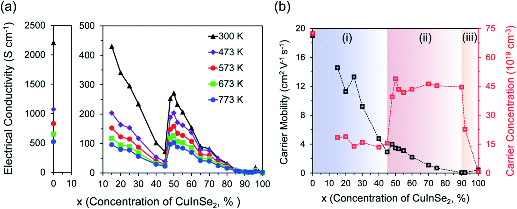 | ||
| Fig. 4 (a) Dependence of electrical conductivity on concentration of CuInSe2 phase at different temperatures. (b) Hole concentration and mobility of (1 − x) Cu2Se/(x) CuInSe2 composites. The results are categorized into three regions based on the trend of the hole concentration. | ||
While the initial drop in the electrical conductivity of samples with x ≤ 45% can be anticipated from the incorporation of a poorly conductive secondary phase within a highly conductive matrix,24,32–36 the observed sudden large increase for the 48 mol% and 50 mol% CuInSe2, suggests either the formation of a new phase, such as Cu3InSe3, with a different molecular structure and thus different electronic band structure, or a sharp alteration of the electronic band structures of both Cu2Se and CuInSe2 phases, owing to their multiscale hierarchical integration within the (1 − x)Cu2Se/(x)CuInSe2 composites. The former hypothesis can be ruled out, because the XRD, SEM and TEM only show the coexistence of Cu2Se and CuInSe2 phases in the sample with x = 50% and the Cu3InSe3 phase is absent below 1180 K from the Cu2Se–CuInSe2 pseudo binary phase diagram (Fig. S1a†).
Therefore, the unusual phase-dependent behavior of the electrical conductivity of (1 − x)Cu2Se/(x)CuInSe2 composites must be rationalized by assuming the alteration of the original electronic band structure of the constituent phases to form a hybrid electronic structure as discussed below. However, we must first elucidate the underlying physics governing the observed change in the electrical conductivity of various samples. Since the electrical conductivity is directly related to carrier concentration (PH) and mobility (μH), σ = ePHμH, it is necessary to investigate how PH and μH change with the compositions. Therefore, Hall effect measurement at 300 K on selected samples was conducted to extract the Hall coefficient (RH). The carrier concentration and mobility were then obtained using PH = 1/(eRH) and μH = σRH, where σ and e are the electrical conductivity and the elementary charge, respectively. All samples show positive RH values at 300 K indicating holes as majority charge carriers (Fig. S8†). At 300 K, pristine Cu2Se displays a hole concentration of 7.2 × 1020 cm−3 and hole mobility of 19 cm2 V−1 s−1(Fig. 4b), both of which are comparable to the values in the literature.20,37 On the other hand, pure CuInSe2 exhibits a significantly lower hole concentration (∼8 × 1018 cm−3) and hole mobility (∼0.5 cm2 V−1 s−1) compared to pristine Cu2Se, which explains its inferior electrical conductivity value. Similar to the phase-dependent electrical conductivity (Fig. 4a), the variation of the carrier concentration and carrier mobility of (1 − x)Cu2Se/(x)CuInSe2 composites with increasing CuInSe2 content (x values) can be divided into three regions. For compositions with x ≤ 45%, the carrier concentration of various composites remains nearly constant at ∼1.5 × 1020 cm−3, whereas the carrier mobility drastically decreases from 14 cm2 V−1 s−1 for the sample with x = 15% to 3 cm2 V−1 s−1 for the sample with x = 45%. The large drop in the carrier mobility suggests that the initial drop in the electrical conductivity of (1 − x)Cu2Se/(x)CuInSe2 composites with x ≤ 45% likely originates from the increased scattering of free carriers at the Cu2Se/CuInSe2 interfaces between α-Cu2Se matrix and CuInSe2 inclusions rather than by a drop in the carrier density within the Cu2Se matrix. Within this composition range, the Cu2Se-matrix is largely dominated by the α-Cu2Se phase, which is doped through partial dissolution of elemental In within its crystal lattice, giving rise to incoherent α-Cu2Se/CuInSe2 interfaces. This explains the drop in the carrier mobility of (1 − x)Cu2Se/(x)CuInSe2 composites with x ≤ 45% as well as their lower carrier density compared to pristine Cu2Se.
For compositions with 45% < x ≤ 90%, a sudden increase in the carrier concentration from ∼1.5 × 1020 cm−3 for x = 45% to ∼4.0 × 1020 cm−3 (x = 48%) and then to ∼5.0 × 1020 cm−3 (x = 50%) is observed. The carrier concentration then remains constant at ∼4.5 × 1020 cm−3 with further increase in the CuInSe2 content up to x = 90% (Fig. 4b). Within the composition range of 90% ≤ x < 100%, the matrix is dominated by the CuInSe2 phase with Cu2Se acting as inclusions. A sharp drop in the carrier density from ∼4.5 × 1020 cm−3 to ∼2.3 × 1020 cm−3 is observed upon increasing the CuInSe2 content from x = 90% to x = 92%. Note that the carrier density for the composition with x = 92% remains ∼29 times larger than that of pristine CuInSe2. One can therefore understand the carrier density trend within region (III) as doping of the insulating CuInSe2 phase by electronic defects from the Cu2Se phase.
The carrier density and mobility phase diagram at 300 K, illustrated in Fig. 4b, sheds light on the unusual dependence of the electrical conductivity of (1 − x)Cu2Se/(x)CuInSe2 composites on the CuInSe2 phase fraction. For instance, it is now evident from this data that the enhancement in the electrical conductivity observed for samples with x = 48% and 50% originates from the large increase in the carrier concentration. One explanation of the observed increase in the carrier density of samples with 48% ≤ x ≤ 90%, compared to the sample with x = 45% could be the increase in the fractions of β-Cu2Se within these samples, owing to its highly disordered and mobile Cu+ ions. However, the strength of such explanation is diminished by the observed marginal increase in the carrier mobility for samples with x = 48% and x = 50% compared to the sample with x = 45%. This is because the large increase in carriers scattering (carrier–carrier scattering as well as carrier scattering by mobile Cu+ ions) that would normally result from the increase in hole density, and Cu disorder should lead to a drastic reduction in the carrier mobility rather than the observed marginal increase in carrier mobility. Therefore, a more complex doping mechanism, which considers the electronic interaction between the coexisting Cu2Se and CuInSe2 phases, must be explored to rationalize the observed surprising increase in both the carrier density and carrier mobility for the samples with x = 48% and 50%, as discussed below.
3.3. Band picture for hierarchical composites
To explore the interactions of electronic defects in composites consisting of Cu2Se and CuInSe2, it is imperative to first understand the impurity defects in individual components. CuInSe2 initially behaves like a weakly degenerate semiconductor from 300–500 K (Fig. S6 and S7a†). This indicates the existence of a shallow acceptor level, which is already ionized at comparatively low temperatures. Since the lowest acceptor level in CuInSe2 (CIS) is copper vacancy, [VCu]CIS− with the activation energy of only 0.03 eV,38 it is reasonable to deduce that Cu vacancies in the CuInSe2 phase are ionized at 300 K. Increasing the temperature enhances carrier scattering, leading to the observed decreasing trend in the electrical conductivity. Once the temperature rises above 500 K, the electrical conductivity shows an interesting increasing trend in CuInSe2, which is similar to the reports on other chalcopyrites, such as (Cu,Ag)(In,Ga)Te2,39–41 and it is believed to be related to in-gap deeper acceptor levels. To understand the essence of the thermally activated conduction, the electrical conductivity of CuInSe2 at high temperature was assessed using the Arrhenius equation:where σ0 is the conductivity at infinite temperature, Ea is the activation energy, and kB is the Boltzmann constant.32,34 The activation energy is found to be ∼0.2 eV, which is much smaller than the well-known band gap of CuInSe2 (1.04 eV

![[thin space (1/6-em)]](https://www.rsc.org/images/entities/char_2009.gif) 42,43), corroborating the assumption that another defect acceptor state is present in between the valence and conduction bands. Therefore, when the temperature increases, electrons are excited to the acceptor state leaving behind free holes in the valence band, which leads to an increase of the electrical conductivity. Once the acceptor state is fully occupied at 740 K, the conductivity enters the saturation range (Fig. S6†). By comparing our result with the theoretically predicted values of the defect energy level in CuInSe2, we conclude that this acceptor state is likely from [VIn]CIS−, which was calculated to be at around 0.17 eV above the Ev.38
42,43), corroborating the assumption that another defect acceptor state is present in between the valence and conduction bands. Therefore, when the temperature increases, electrons are excited to the acceptor state leaving behind free holes in the valence band, which leads to an increase of the electrical conductivity. Once the acceptor state is fully occupied at 740 K, the conductivity enters the saturation range (Fig. S6†). By comparing our result with the theoretically predicted values of the defect energy level in CuInSe2, we conclude that this acceptor state is likely from [VIn]CIS−, which was calculated to be at around 0.17 eV above the Ev.38
Similar analyses can be conducted on composites with x = 90% and 94% and the results are presented in Fig. S7b.† It shows that the carrier activation energy continues to decrease linearly from 0.2 eV for 100% CuInSe2 to 0.06 eV for 90% CuInSe2. This rapid decline in the activation energy again points to the significant influence of Cu2Se on the electronic structure of CuInSe2. Since CuInSe2 does not have additional acceptor states between the aforementioned [VCu]CIS− and [VIn]CIS− states, the origin for this significant decrease in activation energy with just 10% Cu2Se addition must be the incorporation of extrinsic [VCu]CS− acceptor states by the Cu2Se (CS) phase. This analysis is reasonable, because it is well-known that Cu vacancies are generated easily in Cu2Se due to its negative formation energy.37,44 The low activation energy of Cu vacancies and its high density also explain why Cu2Se shows a heavily doped semiconducting behavior (Fig. S6†), despite its moderate band gap of 1–1.2 eV reported for α-Cu2Se.45,46
Strengthened by this knowledge of the distribution of various acceptor states in Cu2Se and CuInSe2, the band structures for the pristine phases are schematically illustrated in Fig. 5a and b. It is also worthwhile to note that, besides the defect levels mentioned above, new defects can form upon integrating Cu2Se and CuInSe2 phases together. Indeed, a careful evaluation of the elemental concentrations in Cu2Se and CuInSe2 phases (Table S1†) reveals that Cu2Se is always Cu-poor, while CuInSe2 is Cu-rich, suggesting diffusion of Cu from Cu2Se to CuInSe2. These off-stoichiometries can also result in the formation of antisite defects [CuIn]CIS− in CuInSe2, which is a much deeper acceptor state with the activation energy of 0.29 eV above Ev.38
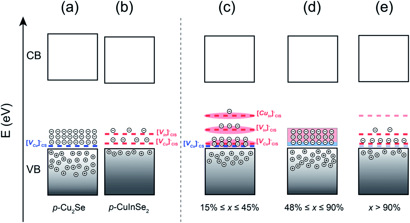 | ||
| Fig. 5 Schematic band structures for (a) pure Cu2Se, (b) CuInSe2, and (1 − x)Cu2Se/(x)CuInSe2 composites with (c) 15% ≤ x ≤ 45%, (d) 48% ≤ x ≤ 90% and (e) x > 90%. The blue and red dashed lines are acceptor states in Cu2Se and CuInSe2, respectively. The acceptor state in Cu2Se is [VCu]CS−. The lower-level acceptor state in CuInSe2 is [VCu]CIS−, while the higher ones are [VIn]CIS− and [CuIn]CIS−. The pink shaded areas demonstrate the band broadening effect with the increasing amount of CuInSe2. The connected strips in (d) represents the formation of an interband by the shallow and deep acceptor states through hybridization. The semitransparent dashed lines in (e) means a gradual disappearance of [VCu]CS− and [CuIn]CIS− states. | ||
To rationalize the unexpected change in the electronic properties observed for (1 − x)Cu2Se/(x)CuInSe2 composites, we propose a band picture illustrated in Fig. 5c–e, which takes into account the distribution of electronic defects from both Cu2Se and CuInSe2 phases. This assumes that the multiscale hierarchical integration of Cu2Se and CuInSe2 phases at both nanometer and micrometer scales in various samples facilitates the interaction of their electronic structures leading to the integration and merging of their work functions. This results in the incorporation of both the shallow acceptor state from the Cu2Se phase ([VCu]CS−) and the shallow and deep acceptor states from the CuInSe2 phase ([VCu]CIS−, [VIn]CIS−, [CuIn]CIS−) within the narrow band gap of the (1 − x)Cu2Se/(x)CuInSe2 hierarchical nanocomposites.
For composites with low CuInSe2 content (15% ≤ x ≤ 45%), the three acceptor states from CuInSe2 coexist with the acceptor state in Cu2Se as discrete states. However, only [VCu]CS− and [VCu]CIS− acceptor states are ionized at 300 K given their low activation energies. The deeper acceptor states, [VIn]CIS− and [CuIn]CIS−, are not much accessible to thermally excited electrons from the VB at 300 K. Because the density of [VCu]CS− defects is greater in Cu2Se than the [VCu]CIS− in the CuInSe2 phase and the former is not fully compensated by the latter, the overall hole density in (1 − x)Cu2Se/(x)CuInSe2 hierarchical nanocomposites initially decreases rapidly upon incorporation of a small fraction of CuInSe2 (x < 15%). As the fraction of CuInSe2 phase reaches the percolation limit, x ≥ 15%, the higher density of point defects leads to band broadening47–50 of the defect levels, which effectively decreases their activation energies (Fig. 5c). Therefore, an increase in the fraction of the CuInSe2 phase within the range 15% ≤ x ≤ 45% does not significantly change the concentration of point defects that are accessible to thermally excited carrier at 300 K, since the extrinsic [VCu]CIS−, [VIn]CIS−, [CuIn]CIS− defects incorporated from the CuInSe2 phase balanced the reduction in the fraction of [VCu]CS− resulting from the decrease in the fraction of the Cu2Se phase. This explains the relatively constant value of the hole density at 300 K for composites within the range 15% ≤ x ≤ 45%. However, all the point defects contribute to carriers scattering along with the high density of α-Cu2Se/CuInSe2 interfaces. This explains the observed drastic decrease in the carrier mobility and the electrical conductivity (Fig. 4) upon increasing the content of CuInSe2 from x = 15% to x = 45%.
For samples approaching the equimolar compositions (48% ≤ x ≤ 52%), the observed unique electronic behavior when compared to samples with x ≤ 45%, such as the 3-fold increase in both the electrical conductivity and the carrier density, suggests a significant change in the electronic band structure. For instance, the sharp increase in the carrier density implies that deep acceptor states in those samples are now accessible by thermally excited carriers from the VB of the Cu2Se matrix, and therefore contribute to the electronic conduction. One possible change in the electronic band structure that would lead to such an increase in the density of accessible acceptor states is the formation of an inter-band (IB) with impurity states distributed within a narrower energy range as illustrated in Fig. 5d. As mentioned above, the acceptor states from CuInSe2 would experience band broadening, and their resultant bandwidth would increase with the increasing x value (increasing density of point defects). Specifically, the deeper acceptor defect, [CuIn]CIS−, whose concentration depends on both the fraction of Cu2Se and CuInSe2 phases, will likely reach the maximum concentration near the equimolar composition. Therefore, it is possible that within this composition range, a critical point for impurity bands variation is reached, where orbitals of deep acceptor states can partially overlap with those of the shallow acceptor states, leading to some degree of hybridization. This mechanism explains well the concurrent increase in the carrier density and carrier mobility. Since the hybridization of impurity states, arising from the integration and merging of electronic band structures of both phases, increases the density of available acceptor states while eliminating the energy barrier at the interfaces, it minimizes carrier scattering. The formation of such an inter-band of hybridized impurity states is presumably a consequence of the high degree of intermixing that results from the hierarchical integration of both Cu2Se and CuInSe2 phases with nearly equimolar ratio. The intimate contact between both phases at the atomic, nanometer and micron scales in the hierarchical structure effectively facilitates the merging of their band structures. Therefore, one can conclude from this analysis that the deviation from the anticipated monotonic change of hole concentration with increasing CuInSe2 content is a manifestation of a more complex interactions between Cu2Se and CuInSe2 owing to their unique hierarchical micro-structure, rather than merely a consequence of the elemental doping effect reported in other composites consisting of Cu2Se and copper metal chalcogenides18,19,51
For compositions in the range 52% ≤ x ≤ 90%, the band hybridization progresses, while the concentration of [VCu]CS− from Cu2Se continues to decrease. These two trends counteract each other and help maintain an almost constant carrier concentration. Meanwhile, the carrier mobility decreases with the increasing CuInSe2 content, which explains the observed drop in the electrical conductivity within this composition range (Fig. 4a). The drop in the carrier mobility with increasing x value within this composition range, where the CuInSe2 phase dominates, can be attributed to the intensified carrier scattering due to the increase in the density of ionized deep acceptor defects from CuInSe2 phase within the band gap. This is in contrast to the scattering of carriers at α-Cu2Se/CuInSe2 interfaces, as proposed above for compositions with low CuInSe2 content (x ≤ 45%). Cubic β-Cu2Se and tetragonal CuInSe2 have similar lattice parameters at the ab plane with <1% difference (a = 5.833 Å for β-Cu2Se; a = b = 5.796 Å for CuInSe2). This leads to a high degree of coherency between CuInSe2 and β-Cu2Se in those samples which mitigates carrier scattering. However, the increased phase fraction of CuInSe2 contributes to a higher density of electronic defects, such as [VCu]CIS−, [VIn]CIS−, and [CuIn]CIS−, leading to increased carrier–impurity scattering.
For compositions with x > 90%, the decreasing presence of the Cu2Se phase eventually leads to the disappearance of [VCu]CS− defects from Cu2Se and a rapid drop in the fraction of [CuIn]CIS− acceptor states from CuInSe2, as illustrated by the semitransparent dashed lines in Fig. 5e. This explains the observed rapid drop in the hole density. In the meantime, a slight enhancement in carrier mobility is observed, which is due to the elimination of the β-Cu2Se as the secondary phase in the CuInSe2 matrix. Owing to the semi-coherent interfaces between those two phases, the increase in the carrier mobility is minimal.
Overall, the hierarchical structural integration of Cu2Se and CuInSe2 phases together with the hybridization between their native acceptor states explains the intriguing behavior in the carrier concentration and electrical conductivity observed in various composites in the range of 48% ≤ x ≤ 90%.
4. Conclusions
We have demonstrated an elegant approach to construct a bulk hierarchical structure in the (1 − x)Cu2Se/(x)CuInSe2 composites, where domains from Cu2Se and CuInSe2 phases are mutually integrated from nano to micron scale. Using temperature dependent electrical conductivity data on 23 samples and carrier concentration data on selected samples in the composition range 15% ≤ x ≤ 100%, we established the electronic transport phase diagram for the (1 − x)Cu2Se/(x)CuInSe2 composites. We found that the CuInSe2 content has a great influence on the microstructure as well as on the electronic properties of various composites. For instance, the degree of intermixing between Cu2Se-rich and CuInSe2-rich domains can be tuned from Cu2Se-rich matrix/CuInSe2-inclusions for compositions with x ≤ 45% (region I) to CuInSe2-matrix/Cu2Se-inclusions for compositions with x > 90% (region III) through systematic variation of the phase ratio (Cu2Se:CuInSe2). The maximum level of intermixing was observed for near equimolar compositions where both Cu2Se and CuInSe2 phases can simultaneously be regarded as the inclusions and as the matrices. Variations in the electrical conductivity with changes in the phase concentration detected over a broad range of temperatures (300–773 K) featured an unusual trend. An initial rapid decrease in the electrical conductivity with the increasing CuInSe2 content was observed for compositions with x ≤ 45% (region I), then a sudden large increase in the conductivity was observed in phases having near equimolar compositions, followed by a weaker drop thereafter. Carrier concentration and mobility phase diagrams revealed that while the rapid decrease in the electrical conductivity for compositions with x ≤ 45% is largely due to a fast drop in the carrier mobility, the sudden increase in the electrical conductivity for near equimolar compositions and the subsequent weaker drop are consequences of the unexpected large increase in the carrier density of samples with 48% ≤ x ≤ 90% (region II). Such an unusual increase in the carrier density is interpreted as a manifestation of the formation of an inter-band of hybridized impurity states due to the complex interactions between intrinsic acceptor states from Cu2Se and CuInSe2 phases, which is presumably facilitated by their unique hierarchical integration. Our work not only provides electronic phase diagrams for the (1 − x)Cu2Se/(x)CuInSe2 system as a potential multifunctional composite, but it also introduces hierarchically integrated phases as a new design approach to couple multifunctionalities in bulk composite materials, which may pave the way to uncover new and exciting physical properties.
Conflicts of interest
The authors declare no competing financial interest.Acknowledgements
This work was supported by the Department of Energy, Office of Basic Energy Sciences under Award # DE-SC-00018941. This work made use of the TEM from the Michigan Materials Characterization Center, (MC)2, purchased with funds from the National Science Foundation Awards (DMR-0723032).References
- I. M. Ross, Proc. IEEE, 1998, 86, 7–28 CrossRef.
- H. J. Queisser and E. E. Haller, Science, 1998, 281, 945–950 CrossRef CAS PubMed.
- E. R. Weber, Phys. B, 2003, 340, 1–14 CrossRef.
- E. G. Seebauer and K. W. Noh, Mater. Sci. Eng., R, 2010, 70, 151–168 CrossRef.
- J. B. Yi, C. C. Lim, G. Z. Xing, H. M. Fan, L. H. Van, S. L. Huang, K. S. Yang, X. L. Huang, X. B. Qin, B. Y. Wang, T. Wu, L. Wang, H. T. Zhang, X. Y. Gao, T. Liu, A. T. S. Wee, Y. P. Feng and J. Ding, Phys. Rev. Lett., 2010, 104, 137201 CrossRef CAS PubMed.
- P. Wachter and E. Kaldis, Solid State Commun., 1980, 34, 241–244 CrossRef CAS.
- C. H. Wang, W. S. Liao, Z. H. Lin, N. J. Ku, Y. C. Li, Y. C. Chen, Z. L. Wang and C. P. Liu, Adv. Energy Mater., 2014, 4, 1400392 CrossRef.
- Z. Z. Wang, J. Clayhold, N. P. Ong, J. M. Tarascon, L. H. Greene, W. R. McKinnon and G. W. Hull, Phys. Rev. B: Condens. Matter Mater. Phys., 1987, 36, 7222 CrossRef CAS PubMed.
- Y. Zhao, J. S. Dyck, B. M. Hernandez and C. Burda, J. Am. Chem. Soc., 2010, 132, 4982–4983 CrossRef CAS PubMed.
- H. Anno, K. Matsubara, Y. Notohara, T. Sakakibara and H. Tashiro, J. Appl. Phys., 1999, 86, 3780–3786 CrossRef CAS.
- M. Balkanski and R. F. Wallis, Semiconductor physics and applications, Oxford University Press, 2000 Search PubMed.
- C. G. Van De Walle, D. B. Laks, G. F. Neumark and S. T. Pantelides, Phys. Rev. B: Condens. Matter Mater. Phys., 1993, 47, 9425 CrossRef CAS PubMed.
- T. J. Smart, V. U. Baltazar, M. Chen, B. Yao, K. Mayford, F. Bridges, Y. Li and Y. Ping, Chem. Mater., 2021, 33, 4390–4398 CrossRef CAS.
- S. Jana, B. B. Srivastava, S. Jana, R. Bose and N. Pradhan, J. Phys. Chem. Lett., 2012, 3, 2535–2540 CrossRef CAS PubMed.
- N. Pradhan, S. Das Adhikari, A. Nag and D. D. Sarma, Angew. Chem., Int. Ed., 2017, 56, 7038–7054 CrossRef CAS.
- F. P. García de Arquer, D. V. Talapin, V. I. Klimov, Y. Arakawa, M. Bayer and E. H. Sargent, Science, 2021, 373, eaaz8541 CrossRef PubMed.
- A. A. Olvera, N. A. Moroz, P. Sahoo, P. Ren, T. P. Bailey, A. A. Page, C. Uher and P. F. P. Poudeu, Energy Environ. Sci., 2017, 10, 1668–1676 RSC.
- R. Lu, A. Olvera, T. P. Bailey, C. Uher and P. F. P. Poudeu, ACS Appl. Mater. Interfaces, 2020, 12, 58018–58027 CrossRef CAS.
- R. Lu, T. P. Bailey, C. Uher and P. F. P. Poudeu, ACS Appl. Energy Mater., 2020, 3, 9133–9142 CrossRef CAS.
- H. Liu, X. Shi, F. Xu, L. Zhang, W. Zhang, L. Chen, Q. Li, C. Uher, T. Day and J. Snyder, Nat. Mater., 2012, 11, 422–425 CrossRef CAS PubMed.
- L. Yang, Z. G. Chen, G. Han, M. Hong, Y. Zou and J. Zou, Nano Energy, 2015, 16, 367–374 CrossRef CAS.
- L. L. Zhao, X. L. Wang, J. Y. Wang, Z. X. Cheng, S. X. Dou, J. Wang and L. Q. Liu, Sci. Rep., 2015, 5, 1–6 Search PubMed.
- D. Byeon, R. Sobota, K. Delime-Codrin, S. Choi, K. Hirata, M. Adachi, M. Kiyama, T. Matsuura, Y. Yamamoto, M. Matsunami and T. Takeuchi, Nat. Commun., 2019, 10, 1–7 CrossRef PubMed.
- F. O. Adurodija, M. J. Carter and R. Hill, Sol. Energy Mater. Sol. Cells, 1996, 40, 359–369 CrossRef CAS.
- A. Rockett and R. W. Birkmire, J. Appl. Phys., 1991, 70, R81–R97 CrossRef CAS.
- H. Bai, J. Wu, X. Su, H. Peng, Z. Li, D. Yang, Q. Zhang, C. Uher and X. Tang, Nat. Commun., 2021, 12, 1–6 CrossRef PubMed.
- A. Olvera, P. Sahoo, S. Tarczynski and P. F. P. Poudeu, Chem. Mater., 2015, 27, 7179–7186 CrossRef CAS.
- J. B. Rivest, L. Fong, P. K. Jain, M. F. Toney and A. P. Alivisatos, J. Phys. Chem. Lett., 2011, 2, 2402–2406 CrossRef CAS.
- Y. Li, W. Qi, Y. Li, E. Janssens and B. Huang, J. Phys. Chem. C, 2012, 116, 9800–9804 CrossRef CAS.
- A. Sahu, D. Braga, O. Waser, M. S. Kang, D. Deng and D. J. Norris, Nano Lett., 2014, 14, 115–121 CrossRef CAS.
- R. C. Garvie and M. F. Goss, J. Mater. Sci., 1986, 21, 1253–1257 CrossRef CAS.
- M. Varela, J. L. Morenza, J. Esteve and J. M. Codina, J. Phys. D: Appl. Phys., 1984, 17, 2423–2427 CrossRef CAS.
- S. C. Park, S. H. Kwon, J. S. Song and B. T. Ahn, Sol. Energy Mater. Sol. Cells, 1998, 50, 43–49 CrossRef CAS.
- T. Datta, R. Noufi and S. K. Deb, Appl. Phys. Lett., 1985, 47, 1102–1104 CrossRef CAS.
- R. R. Philip, B. Pradeep, G. S. Okram and Y. Ganesan, Semicond. Sci. Technol., 2004, 19, 798–806 CrossRef CAS.
- M. A. Abdullaev, D. K. Magomedova, R. M. Gadzhieva, E. I. Terukov, Y. A. Nikolaev, Y. V. Rud’ and P. P. Khokhlachev, Semiconductors, 2001, 35, 870–872 CrossRef CAS.
- J. Y. Tak, W. H. Nam, C. Lee, S. Kim, Y. S. Lim, K. Ko, S. Lee, W. S. Seo, H. K. Cho, J. H. Shim and C. H. Park, Chem. Mater., 2018, 30, 3276–3284 CrossRef CAS.
- S. B. Zhang, S. H. Wei, A. Zunger and H. Katayama-Yoshida, Phys. Rev. B: Condens. Matter Mater. Phys., 1998, 57, 9642 CrossRef CAS.
- Y. Cao, X. Su, F. Meng, T. P. Bailey, J. Zhao, H. Xie, J. He, C. Uher and X. Tang, Adv. Funct. Mater., 2020, 30, 2005861 CrossRef CAS.
- H. Xie, S. Hao, S. Cai, T. P. Bailey, C. Uher, C. Wolverton, V. P. Dravid and M. G. Kanatzidis, Energy Environ. Sci., 2020, 13, 3693–3705 RSC.
- H. Xie, S. Hao, T. P. Bailey, S. Cai, Y. Zhang, T. J. Slade, G. J. Snyder, V. P. Dravid, C. Uher, C. Wolverton and M. G. Kanatzidis, J. Am. Chem. Soc., 2021, 143, 5978–5989 CrossRef CAS PubMed.
- H. T. Shaban, M. Mobarak and M. M. Nassary, Phys. B, 2007, 389, 351–354 CrossRef CAS.
- A. J. Nelson, A. B. Swartzlander, J. R. Tuttle, R. Noufi, R. Patel and H. Höchst, J. Appl. Phys., 1993, 74, 5757–5760 CrossRef CAS.
- X. Zhao, S. Ning, N. Qi, Y. Li, Y. Dong, H. Zhang, J. Liu, B. Ye and Z. Chen, ACS Appl. Mater. Interfaces, 2021, 13, 58936–58948 CrossRef CAS PubMed.
- G. K. Padam, Thin Solid Films, 1987, 150, 89–92 CrossRef.
- H. Chi, H. Kim, J. C. Thomas, G. Shi, K. Sun, M. Abeykoon, E. S. Bozin, X. Shi, Q. Li, X. Shi, E. Kioupakis, A. Van Der Ven, M. Kaviany and C. Uher, Phys. Rev. B: Condens. Matter Mater. Phys., 2014, 89, 1–5 Search PubMed.
- T. F. Lee and T. C. McGill, J. Appl. Phys., 1975, 46, 373–380 CrossRef CAS.
- S. R. Dhariwal, V. N. Ojha and G. P. Srivastava, IEEE Trans. Electron Devices, 1985, 32, 44–48 Search PubMed.
- E. Arushanov, J. H. Schön, H. Matsushita and T. Takizawa, Phys. Status Solidi, 1999, 176, 1009–1016 CrossRef CAS.
- L. Essaleh, S. M. Wasim and J. Galibert, J. Appl. Phys., 2001, 90, 3993–3997 CrossRef CAS.
- F. S. Liu, Z. N. Gong, M. J. Huang, W. Q. Ao, Y. Li and J. Q. Li, J. Alloys Compd., 2016, 688, 521–526 CrossRef CAS.
Footnote |
| † Electronic supplementary information (ESI) available: Fig. S1 to S8 and Table S1. See https://doi.org/10.1039/d2na00230b |
| This journal is © The Royal Society of Chemistry 2022 |