
 Open Access Article
 This Open Access Article is licensed under a Creative Commons Attribution-Non Commercial 3.0 Unported Licence
A fine single Pd microwire H2 sensor fabricated by using a femtosecond laser for a wide detection range at room temperature†
He
Zhu‡
,
Yun-Zhi
Dai‡
,
Xiang-Chao
Sun
and
Hong
Xia
 *
*
State Key Laboratory of Integrated Optoelectronics, College of Electronic Science and Engineering, Jilin University, 2699 Qianjin Street, Changchun, 130012, China
First published on 29th August 2022
Abstract
We reported a fine H2 sensor based on single Pd microwires (SPMs) by femtosecond-laser-induced deposition of palladium nanoparticles (PdNPs), which exhibits excellent H2 sensing performance. The PdNPs with good dispersion were prepared by ultrasonic assisted one-step solution synthesis. The sensor has a wide detection range of 0.001–4.0% H2 sensing at room temperature. With the increase of the H2 concentration, the SPM sensor presents two sensing mechanisms, the formation of PdHx and hydrogen induced lattice expansion regulating the conductivity of SPMs. This fine hydrogen sensor is promising to be applied to human health monitoring, environmental air detection and other integrated intelligent devices.
Introduction
Hydrogen (H2) has become an important subject in science and technology, as it is one of the hopes of future clean energy production. H2 has a wide flammability range (4–75% in air) and a low ignition energy (0.02 mJ), and can release large amounts of energy.1–4 However, H2 leakage is dangerous and not easily detectable since it is colorless and odorless; the damage caused by its explosion cannot be ignored.5,6 Therefore, it is necessary to carry out real-time monitoring of H2 concentrations in the environment or equipment. In H2-related application fields, such as H2 storage and separation, fuel cells and industrial processing, it is required to have high sensitivity, high precision, high reliability and low power consumption, which puts forward high requirements for H2 detection.7,8 Palladium (Pd), as a highly sensitive and selective H2 sensitive material, has been widely used in H2 sensors.9 H2 molecules can be selectively adsorbed on the surface of Pd. Hydrogen atoms decomposed from H2 molecules diffuse to the lattice gap position of Pd,10 resulting a resistance variance of Pd due to the formation of the Pd/H solid solution (α phase) or PdHx (β phase). The transition from the α phase to the β phase happens when the H2 concentration is 1–2% at normal temperature and pressure, with the lattice constant increased by 3.5%.11Numerous Pd-based nanostructures, including Pd thin films, Pd tubes, Pd nanoparticles, and Pd nanowires, have been developed for high sensitivity and selectivity H2 sensors.12–14 However, the common H2 sensors from Pd nanomaterials are centimeter scale devices, which is difficult to meet the requirement of miniaturization and integration. Toward the goal of Internet-of-Things, fine sensors are important with a scale less than millimeters, controllable fabrication and easy integration. In recent years, one-dimensional fine Pd microstructure sensors, such as micro-nanowires and nanotubes, have shown the H2 sensing potential with a low detection limit and low power consumption because of the large specific surface area and high surface reactivity.15,16 Several micro/nano fabrication methods have been used to fabricate one-dimensional Pd microstructures, such as lithographically patterned nanowire electrodeposition (LPNE) and the focused ion/electron beam method.17–19
However, all these preparation methods have certain limitations. For example, the LPNE depends on the electrodeposition of the metal precursor solution down the edges of the sacrificed nickel electrode which is patterned and etched by lithography. The parameters of electrochemical deposition should be controlled strictly, and the steps of repeated attachment and removal of the mask increase the technical difficulty and operation time.13,20–23 Focused ion/electron beam etching may cause damage to the side walls of micro/nanowires due to ion/electron beam lateral bombardment.17 Therefore, it is essential to develop a simple, low-cost and universal technology for the preparation of one-dimensional palladium micro/nanostructures. A fabrication method for a fine H2 sensor with excellent device performance, easy integration, good compatibility and convenient preparation is needed.
Femtosecond laser direct writing (FsLDW) has the advantages of micro/nanometer spatial resolution, an ultralow thermal effect, and excellent geometry designability.24–27 In this paper, we developed a single Pd microwire (SPM) H2 sensor based on femtosecond laser induced deposition of nanoparticles (NPs) from aqueous solution, which has a wide detection range, low measurement line and low power consumption.28,29 The NPs dispersed in solution are induced by a high-energy beam to form a designable and sensitive material pattern. The whole preparation process is digital and does not require any mask, chemical additives or catalysts. The laser-irradiated NPs were deposited stably on the substrate according to the predesigned pattern, while the unirradiated parts are removed from the substrate by rinsing with deionized water. The SPM sensor has good repeatability and a wide detection range for H2 sensing. The sensing mechanisms of the prepared SPM have been investigated. There are two mechanisms in the sensing process, in which PdHx plays a dominant role at low concentrations, and the HILE effect is dominant in a high concentration H2 atmosphere.
Results and discussion
Ultrasound assisted synthesis has been an effective approach to prepare nanomaterials due to the wide applicability range of liquid-based chemical and physical syntheses.30 It is reported for the first time in this paper that palladium nanoparticles (PdNPs) have been synthesized by the one-step ultrasound assisted method. The synthesis scheme of the PdNPs is shown in Fig. 1a. The XRD diffraction pattern of the synthesized PdNPs is shown in Fig. 1b. The peaks with 2θ values of 40.1°, 46.658°, 68.119°, 82.098° and 86.617°, are consistent with the diffraction peaks of the crystal planes (111), (200), (220), (311) and (222) of Pd JCPDS 46-1043, respectively. It can be seen that these diffraction peaks are sharp and strong, indicating the sample with high crystallinity. No other miscellaneous peaks are observed, which proves that the sample is of high purity. The SEM image in Fig. 1c reveals the small flake particles of the PdNPs with good dispersion. The particle size distributions are illustrated in Fig. 1d which certify the uniform size of PdNPs. The diameter is in the range of 25–45 nm.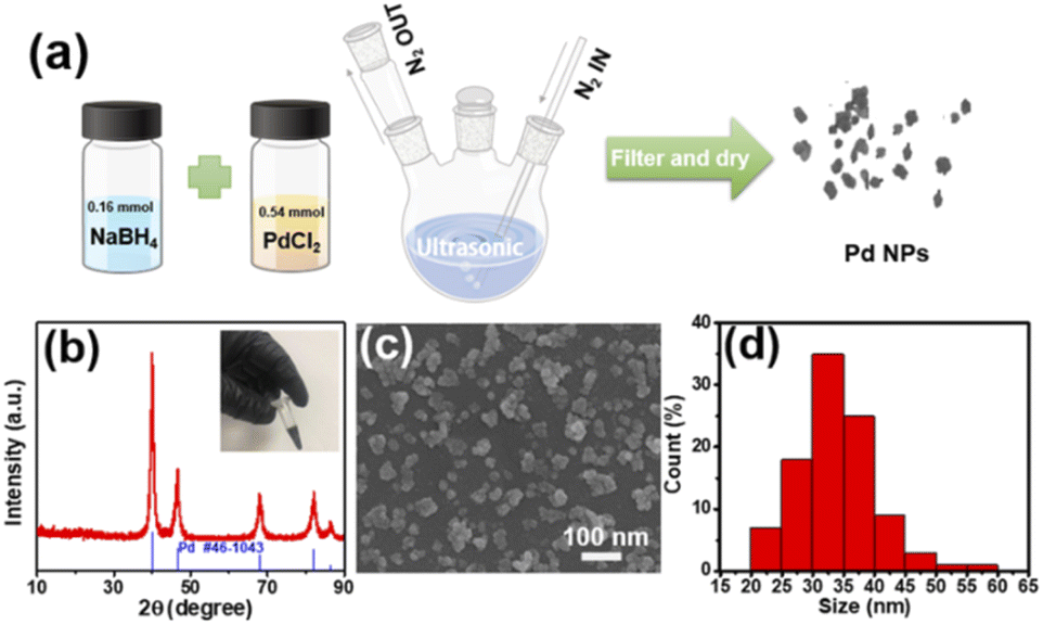 | ||
| Fig. 1 (a) The preparation diagram of PdNPs. (b) The XRD pattern of the synthesized PdNPs; vertical bars denote the standard data of orthorhombic Pd (JCPDS no. 46-1043). (c) The SEM image of the as-synthesized PdNPs. (d) Particle size distribution graph obtained from the SEM image. | ||
A fine H2 sensor was fabricated by laser deposition of the PdNPs from the solution as a sensitive material. Fig. 2a shows the schematic diagram of a SPM sensor fabricated by femtosecond laser processing, which was proved to be an efficient method for micro–nano scale devices.31–36 Here, the laser beam with a certain power is guided by the light path and radiated on the interface between the electrode and the PdNP droplet. The patterned PdNPs were prepared by controlling the scanning path of the 3D processing platform. The micrograph and SEM images of the deposited PdNP microstructures are illustrated in Fig. 2b–d; as can be seen, the SPM can be well connected at both ends of the electrode, and the effective sensitive area is about 5.5 μm × 42.8 μm. Moreover, the interconnection between PdNPs is good, which can form a path. The surface of the nanowires is very rough, and the nanopore formed by the accumulation of particles can be seen clearly (Fig. 2d). In order to obtain well-structured and patterned Pd, it is necessary to control the laser power in the range of 12–25 mW. When Pw > 25 mW, the laser will induce Au@Ge@Ni substrate etching, which will destroy the structural integrity of the deposited material in an aqueous solution environment. Nevertheless, when Pw < 12 mW, the PdNPs could not be welded on the substrate due to the low laser energy. When Pw = 16 ± 0.1 mW and the single point exposure time is 850 μs, FsLDW can induce a PdNP pattern in aqueous solution in one step. Various patterns can be self-assembled by laser-induced deposition of PdNPs. The SEM images of two patterns including bat (Fig. 2e) and rudder (Fig. 2f and g) are shown in Fig. 2e–g, and more patterns are shown in Fig. S2.† Laser induced deposition from the solution and welding of PdNPs into microwires can be observed. The TEM images and SAED images of PdNPs before (left) and after (right) laser processing are illustrated in Fig. 3. As can be observed, the lattice of PdNPs has no obvious change, but after laser radiation, the dispersion between the particles is reduced due to the influence of surface welding.
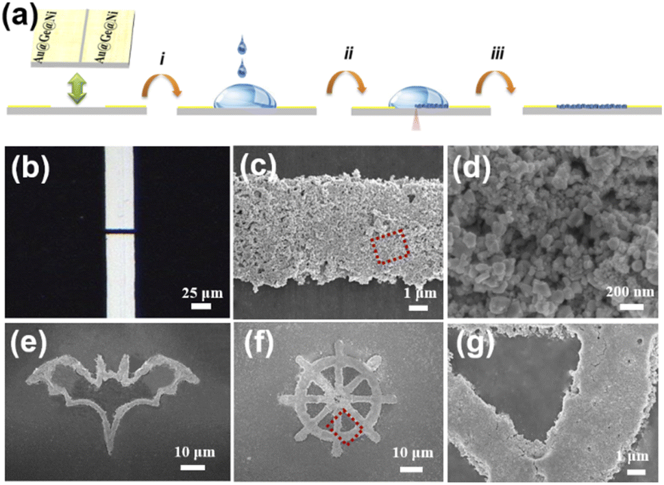 | ||
| Fig. 2 (a) Schematic illustration of the fabrication process of the sensor. (b) Optical micrograph of the SPM. (c) The SEM images of SPMs. (d) The enlarged view of the red square box area in (c). (e and f) The SEM images of cartoon patterns bat and rudder made of Pd. (g) The enlarged view of the red square box area in (f). | ||
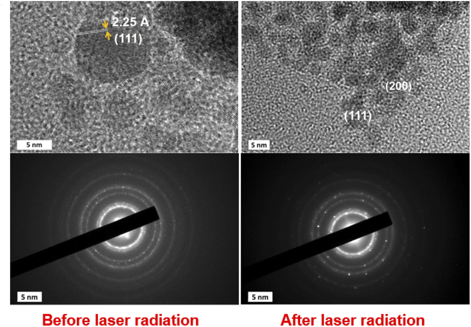 | ||
| Fig. 3 TEM images and SAED images of PdNPs before radiation (left) and after laser radiation (right). | ||
The sensing properties of the fabricated SPMs were studied by H2 exposure with concentrations ranging from 0.001% to 4.0% in N2 at room temperature. Fig. 4 shows the time-dependent response of the SPM sensor to different concentrations of H2 measured at a constant voltage of 100 mV. When the sampling time is 2.5 s, the baseline resistance is 2390 ± 100 Ω. Therefore, the standby power consumption is low, about 4.26 μW. The dynamic response and recovery curves of the SPM sensor exposed to 0.001%, 0.005%, 0.01%, 0.05%, 0.1%, 0.2%, 0.3%, 0.5%, 1.0%, 2.0%, 3.0% and 4.0% H2 in air at room temperature are shown in Fig. 4a–d, respectively. Fig. 4d shows the enlarged dynamic response curve of Fig. 4c in 20–100 s. According to Fig. 4a–c, when the H2 concentration is less than 0.1%, the resistance of the device increases with the increase of H2 concentration (shown in Fig. S3†). When the H2 concentration ranges from 0.1% to 1.0%, the resistance of the device decreases with the increase of H2 concentration (shown in Fig. S4†). And when the H2 concentration is more than 1%, the response curve of H2 is reversed. This is likely due to the competition between the PdHx effect (increasing the device resistance) and the hydrogen induced lattice expansion (HILE) effect (decreasing the device resistance). It can be clearly seen that the resistance of the sensor will increase temporarily when the sensor is exposed to high concentrations of H2, and then the resistance will increase slowly until the response curve reaches the maximum, shown in Fig. 4d. The results show that the PdHx effect and HILE effect exist simultaneously and compete with each other when the sensor is exposed to high concentrations of H2. However, the HILE effect is dominant in the high concentration H2 atmosphere, which leads to the decrease of device resistance and the increase of response current. Furthermore, we separately observe the region where the resistance of the sensor increases temporarily in the high concentration H2 atmosphere (as shown in Fig. 4d). The experiment shows that in this region, with the gradual increase of H2 concentration, the peak shape becomes sharper. This is most likely due to the increase of reactant concentration in high concentration gas, which increases the reaction rate between the gas and sensing material and also has a positive gain effect on the slope of the negative response curve. Based on the above dynamic response curves, it is easy to see that the sensor has different response waveforms at low concentrations and high concentrations of H2, which is very practical and reliable for the electronic nose system which depends on the waveform and slope to detect the gas concentration.
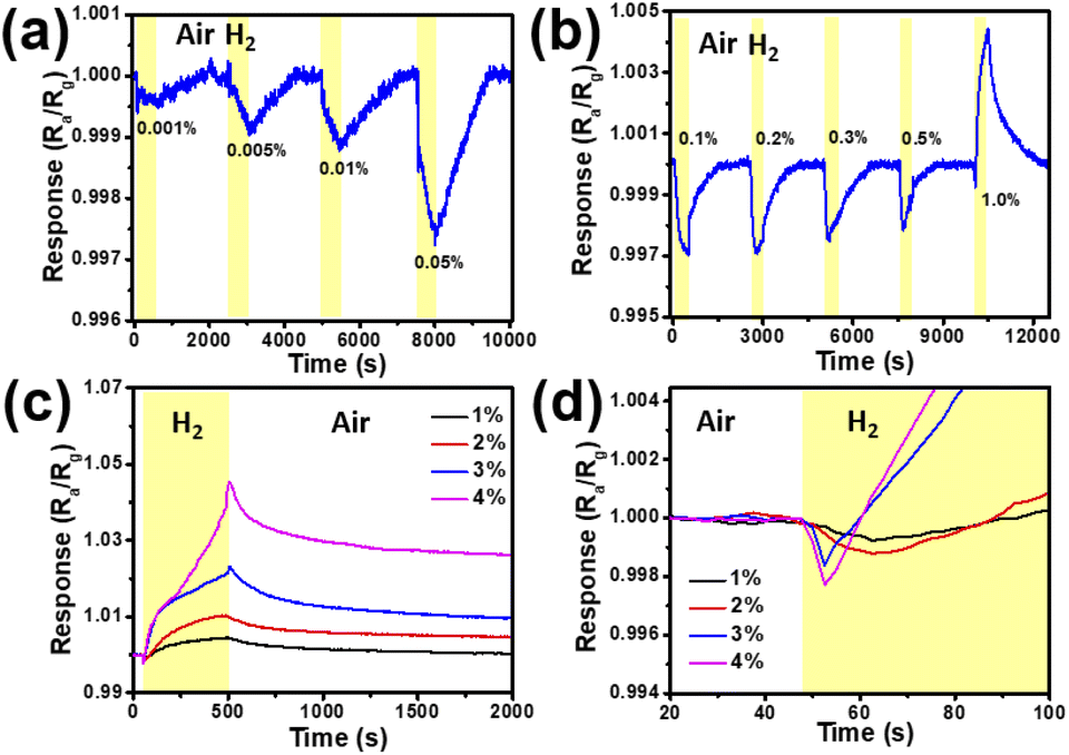 | ||
| Fig. 4 (a–c) Dynamic response and recovery curves of the SPM sensor exposed to 0.001%, 0.005%, 0.01%, 0.05%, 0.1%, 0.2%, 0.3%, 0.5%, 1.0%, 2.0%, 3.0% and 4.0% H2 at room temperature, respectively. (d) The enlarged view of (c) 20–100 s. The area with the yellow background indicates the response of the device under H2, the same as below. | ||
In order to study the response recovery time and sensitivity of the sensors in different H2 concentrations, a series of tests and calculations are carried out, and the results are shown in Fig. 5. The response time and recovery time of the SPM sensor exposed to H2 concentrations of 0.001% to 1.0% at room temperature are shown in Fig. 5a and b. The corresponding responsivity of the sensor in the 0.001–4.0% H2 atmosphere is shown in Fig. 5c. The responses of 0.001%, 0.005%, 0.01%, 0.05%, 0.1%, 0.2%, 0.3%, 0.5%, 1.0%, 2.0%, 3.0% and 4.0% H2 concentrations are 0.00046, 0.00109, 0.0013, 0.00277, 0.003, 0.00293, 0.00242, 0.00213, −0.00446, −0.0102, −0.02245 and −0.04327, respectively. The response of the sensor shows a parabola shape with the increase of H2 concentration, indicating that the sensor was dominated by different sensing mechanisms at low and high concentrations of H2. In addition, the negative response is greater than the positive response, further indicating that lattice expansion can significantly improve the conductivity of Pd. The response time of the device at 1.0–4.0% H2 concentration is shown in Fig. 5d. It can be clearly seen that the change trend of the response time of the sensor at 0.001–1.0% H2 concentrations is similar, that is, with the increase of H2 concentration, the response time and recovery time gradually increase first, then decrease, and then increase again (Fig. S5†). When the H2 concentration is greater than 1.0%, the response time increases with the increase of H2 concentration. When the concentration of H2 is greater than 2.0%, the sensor has a lengthy recovery time or fails to return to the initial value. The main reason is that when exposed to more than 2% H2 concentration, Pd will suffer more than 10% volume expansion,37 resulting in large mechanical stress leading to the displacement of PdNPs.
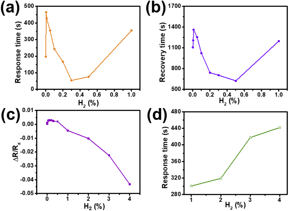 | ||
| Fig. 5 (a) The response time of the SPM sensor exposed to H2 concentrations of 0.001–1.0% at room temperature. (b) The recovery time of the SPM sensor exposed to H2 concentration of 0.001–1.0% at room temperature. (c) The corresponding responsivity of the sensor in the 0.001–4.0% H2 atmosphere. (d) The response time of the device at 1.0–4.0% H2 concentrations. | ||
The dynamic response and recovery curves of the SPM sensor are shown in Fig. 6 at room temperature with the H2 concentration at 0.1%, 0.2%, 1.0% and 2.0%. When the H2 concentration is less than 1.0%, the great dynamic response and recovery curves can be seen in Fig. 6a–c. The results reveal that the SPM sensor still maintains high repeatability after multiple consecutive measurements. It also can be seen from Fig. 6d that although the resistance of the SPM does not return to the initial value at high concentrations, it still has good waveform repeatability, which does not affect the use of devices.
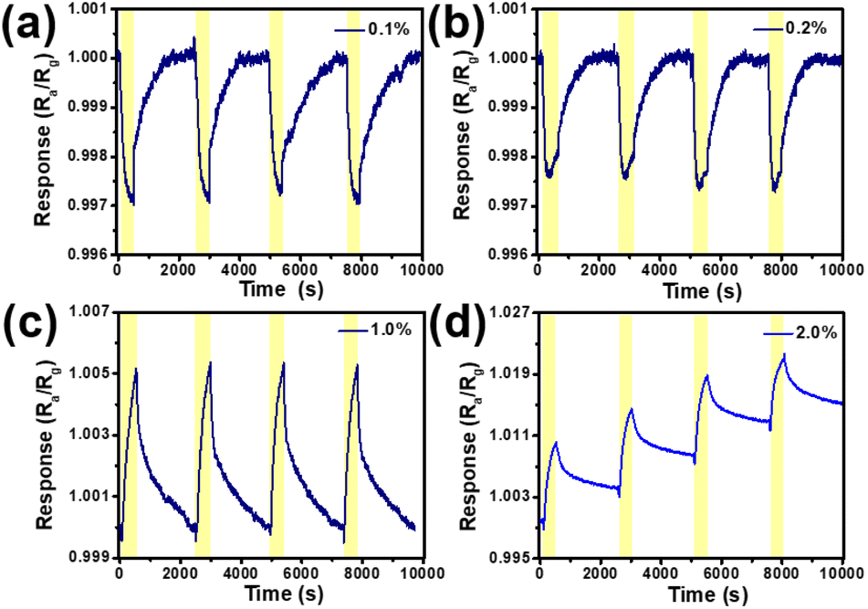 | ||
| Fig. 6 The dynamic response and recovery curves of the SPM sensor at room temperature with the H2 concentration at 0.1% (a), 0.2% (b), 1.0% (c) and 2.0% (d), respectively. | ||
In order to better understand whether the response inversion at high concentrations of H2 is related to the interference of background gas, such as O2 or water molecules in air, we replace the background air with pure N2. Fig. 7a shows the instantaneous response curves of the SPM sensor exposed 2.0% H2 measured in the background gas of N2 and air respectively at room temperature. Fig. 7b is the detailed curve of Fig. 8a at 40–300 s. As can be seen from the curves, the response value of H2 in the background of N2 changes more than that in air, which may be due to the absence of O2 (O2 competes with H2 to adsorb Pd on the surface)21,38 and the interference of water molecules, so that the degree of reaction between H2 and Pd is higher. In addition, the response inversion of the curve still exists, which shows that the response inversion is not due to the interference of O2 or water molecules in air. In order to study the effect of humidity on the SPM sensor, we kept the sensor exposed to 1% hydrogen concentration under different humidity conditions. Different humidity environments were produced by saturated salt solutions in the equilibrium state including CH3COOK for 23% RH, MgCl2 for 32% RH, MgCO3 for 54% RH, NaCl for 75% RH, and KCl for 85% RH. The response of the SPM sensor with different humidities is shown in Fig. 7c. We can see that the resistance changes barely, and humidity plays little role in the response of hydrogen. In order to explore the potential application of the SPM sensors, some interferent gases in the environment (NO2, CO, NH3, and EtOH) are used to verify the selectivity of the SPM sensor. It can be seen from Fig. 7d that the SPM sensor has the highest response to H2 and with a bare response to NO2, CO, NH3, and EtOH. The results indicate that the fabricated SPM sensor has excellent selectivity for H2. This is because H2 molecules can be selectively adsorbed on the surface of Pd. Hydrogen atoms decomposed from H2 molecules diffuse to the lattice gap position of Pd, resulting in a resistance variance of Pd due to the formation of the Pd/H solid solution (α phase) or PdHx (β phase).
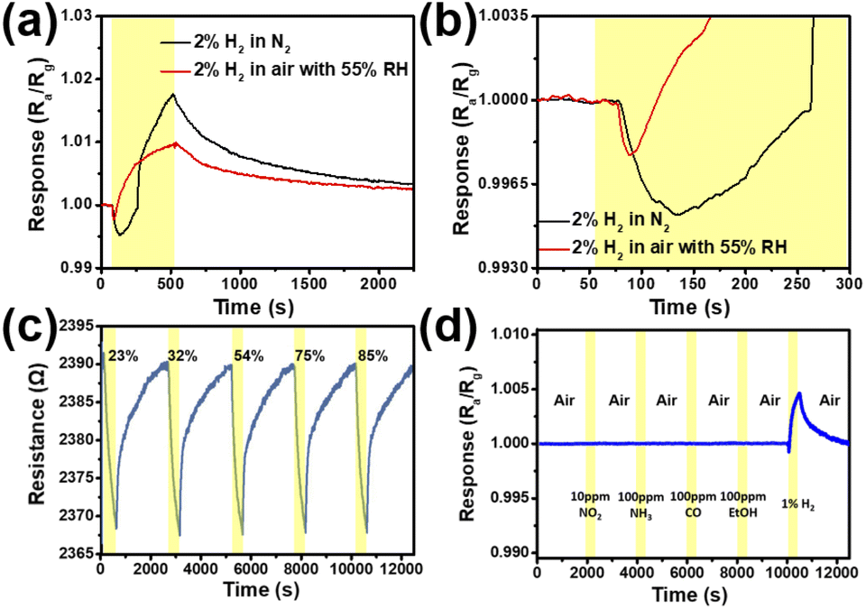 | ||
| Fig. 7 (a) The instantaneous response curves of the SPM sensor exposed to 2.0% H2 measured in the background gas of N2 and air with 55% RH, respectively, at room temperature. (b) The detailed curves of (a) at 40–300 s. (c) The response of the sensor exposed to 1% hydrogen concentration under different humidity conditions from 23% RH to 85% RH at room temperature. (d) Response of the SPM H2 sensor to interferent gases including NO2, NH3, CO and EtOH. | ||
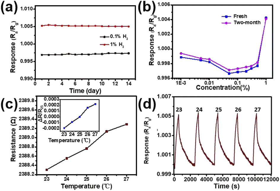 | ||
| Fig. 8 (a) Long-term stability of the SPM H2 sensor exposed to 0.1% and 1% H2. (b) H2 response of the as-fabricated sensor (fresh) and identical sensor (two-month) exposed to ambient conditions for two months. (c) The baseline resistance at temperatures 23 to 27 °C. The inset is the response to temperature variations around the working temperature (25 °C). (d) Response of the SPM sensor to 1% H2 at temperatures 23 to 27 °C. | ||
Repeatability and stability are important indicators for the sensor's practical applications. As shown in Fig. 8a, the initial long-term stability of the SPM sensor exposed to 0.1% and 1% H2 was measured, which shows that there is little change in the response value at 0.1% and 1% H2 . The response remains relatively stable, and the sensor has good stability. The response upon exposure to the H2 concentration from 0.0001% to 1% of the as-fabricated sensor (fresh) and identical sensor (two-month) exposed to ambient conditions for two months is shown in Fig. 8b. Overall, the response has decreased a little after two months of storage under the ambient conditions. However, the response trend has not changed, which does not affect the use of devices. The influence of temperature on the baseline and sensing properties for 1% H2 has been investigated at temperatures in the range of 23 to 27 °C. As shown in Fig. 8c, though the baseline resistance is increased, the change of resistance is less than 1 Ω with a 4 °C change which is equivalent to 0.002% of the initial resistance. Compared with the minimum value of response (0.1%), the change is not one order of magnitude. The response of the SPM H2 sensor to 1% H2 at 23–27 °C is shown in Fig. 8d. There is little fluctuation in the response of the SPM sensor exposed to 1% H2, which shows the feasibility for real applications.
H2 molecule is selectively absorbed on Pd surface and creaking into hydrogen atom.10 Then they diffuse and occupy the gap positions of the Pd lattice, resulting in lattice expansion. Therefore, the resistance of the SPM varies with the Pd/H solid solution (α phase) or PdHx (β phase) formation. This process leads to the formation of PdHx and the increase of electron scattering, which directly results in the increase of Pd resistance.
According to the atomic fraction of PdHx, there are three kinds of phase combination in palladium hydrides: when x < 0.015, there was the α phase only; when 0.015 < x < 0.61, there were two α and β phases together; when x is more than 0.61, there was only the β phase.39 However, lattice expansion plays a more dominant role in the increase of conductivity due to the HILE effect. The lattice expansion rate of the α phase is less than 0.13%.37,40,41 Whether PdHx is α phase or β phase, the conductivity of Pd decreases, and the resistance increases finally. Fig. 9a and b show the AFM images of the SPM deposited by the laser before and after high concentration (>10%) H2 exposure for 15 min. As can be observed, the Pd layer becomes smoother, and the particle size becomes larger, which is similar to the experimental results of X. She et al.42 and D. Gupta et al.43 The mechanism of the negative response (ΔR < 0, Ra > Rg) observed in SPM samples can be described as (Fig. 9c) PdNPs generating a nanometer spacing or voids during the stacking process. As the concentration H2 increases, these nanometer gaps or voids become closer together. With the increase of H2 concentration, the volume of PdNPs gradually increases (related to the volume expansion of Pd caused by phase transition from α to β), which leads to the closure of the gap of PdNPs and a significant increase in electrical conductivity, which is consistent with previous results according to Fig. 4. Hence, PdHx plays a dominant role at low concentrations, and the HILE effect is dominant in a high concentration H2 atmosphere. Different gas-sensitive mechanisms, such as the HILE effect and the formation of PdHx, were probably related to the crystal form and micromorphology of PdNPs.
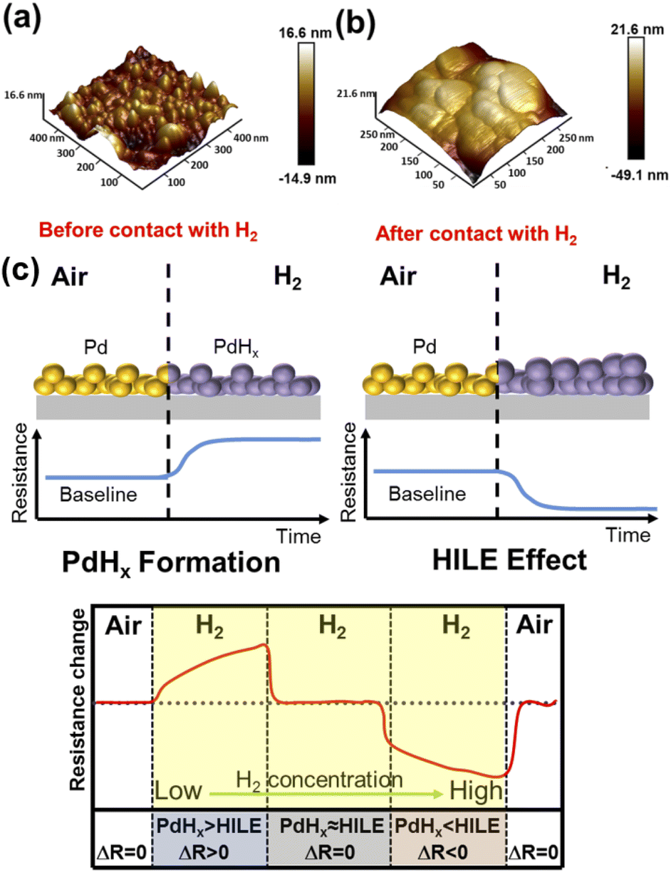 | ||
| Fig. 9 (a and b) The AFM images of the SPM deposited by the laser before and after high concentration (>10%) H2 exposure for 15 min. (c) Schematic diagram of the two sensing mechanisms of the SPM. | ||
Conclusions
In this work, we have synthesized PdNPs with good dispersion by the ultrasonic assisted one-step method. A fine single SPM sensor was fabricated by femtosecond laser induced deposition of the PdNPs. When the H2 concentration is low, PdHx is formed, and a positive resistance response is realized; at a high concentration, the resistance response is negative due to the lattice expansion of PdHx. According to the change of H2 concentration, the sensor presents a highly recognizable induction curve. The sensor has a wide detection range of 0.001–4.0% H2 sensing at room temperature. The arbitrarily patterned microstructure of PdNPs was obtained on the substrate by laser-induced deposition, which could provide a viable fabrication strategy for a miniaturized sensor. The SPM sensor would have great application prospects in the field of integrated chips and e-capsules.Experimental
Materials and characterization
Fabrication of the Pd single microwire
In the femtosecond laser direct writing (FsLDW) processing (Fig. S1†), the laser source with a wavelength at 800 nm, 100 femtosecond pulse width, and a 80 MHz repetition rate was a Ti:sapphire laser system. The laser was focused on the top surface of the cover glass with an inverted oil-immersion objective lens (60×, numerical aperture NA = 1.42). For programmable 3D scanning and fabrication, a piezo stage and a galvanometer scanner were set to control vertical movements and horizontal scanning of the laser beam, respectively. All the fabrication processes were accurately designed with the program (3Ds Max).441 mg synthesised PdNPs was mixed with 5 mL deionized water and then ultrasonicated for half an hour to obtain a suspension that can be stable for a period of time. 25 μL Pd suspension was dropped on the two electrodes with 25–30 nm Au@Ge@Ni alloy and the gap between them. According to the designed structure and scanning mode, the Pd suspension was scanned layer by layer. The single point exposure time was 850 μs, the distance between points, lines and planes was 200 nm, and the processing time was 46 seconds with 5 layers. The laser beam was focused on the interface between the suspension and the cover glass, and the PdNPs were induced to deposit in water by a Fs-laser with 16 ± 0.1 mW power. The suspension without laser radiation was removed by washing with deionized water 5–8 times, and the microstructure on the laser scanning path controlled by the program was left. The Pd-based gas sensor was obtained after drying in air at room temperature for 24 hours.
Gas sensing measurements
H2 sensing of the SPM sensor was at constant temperature and room temperature humidity (25 °C/55% RH). A Keithley source meter (Keithley 2600) was used to monitor the current changes before and after the sensor enters the H2 gas atmosphere under a fixed bias of 0.1 V. When the device current (I0) was stable at a constant voltage (0.1 V), the target H2 was injected into a chamber with 55% RH air through a micro syringe. The H2 and the air were mixed well by electric fans until the detection was completed when the device was exposed to H2 for 450 s. Then, the test chamber was opened, and the sensor was exposed to the atmosphere. The fresh air was replaced with high purity N2 when the background gas was N2. After data processing, the current change value was transformed into the corresponding resistance change value. The gas response was defined as the value of Ra/Rg, where Rg is the sensor resistance with H2 exposure, and Ra is the sensor resistance in air (baseline). The baseline before measurement was checked everytime. The response time is defined as the time from Ra to 90% of Rmax, and the recovery time is defined as the time from Rmax to 10% of Rmax, where Rmax is the resistance measured at 450 s under the targeted gas.Author contributions
The manuscript was written through contributions of all authors. All authors have given approval to the final version of the manuscript.Conflicts of interest
The authors declare no conflict of interest.Acknowledgements
This work was supported by the Natural Science Foundation of Jilin Province # 20220101105JC and the National Key Research and Development Program of China # 62075081.Notes and references
- W. T. Koo, H. J. Cho, D. H. Kim, Y. H. Kim, H. Shin, R. M. Penner and I. D. Kim, ACS Nano, 2020, 14, 14284–14322 CrossRef PubMed.
- Y. Pak, N. Lim, Y. Kumaresan, R. Lee, K. Kim, T. H. Kim, S.-M. Kim, J. T. Kim, H. Lee, M.-H. Ham and G.-Y. Jung, Adv. Mater., 2015, 27, 6945–6952 CrossRef CAS.
- T. Hübert, L. Boon-Brett, G. Black and U. Banach, Sens. Actuators, B, 2011, 157, 329–352 CrossRef.
- A. K. Spiliotis, M. Xygkis, M. E. Koutrakis, K. Tazes, G. K. Boulogiannis, C. S. Kannis, G. E. Katsoprinakis, D. Sofikitis and T. P. Rakitzis, Light: Sci. Appl., 2021, 10, 35 CrossRef CAS.
- R. M. Penner, Acc. Chem. Res., 2017, 50, 1902–1910 CrossRef CAS.
- H.-S. Lee, J. Kim, H. Moon and W. Lee, Adv. Mater., 2021, 2005929 CrossRef CAS.
- A. Haryanto, S. Fernando, N. Murali and S. Adhikari, Energy Fuels, 2005, 19, 2098–2106 CrossRef CAS.
- A. Kolmakov, D. O. Klenov, Y. Lilach, S. Stemmer and M. Moskovits, Nano Lett., 2005, 5, 667–673 CrossRef CAS PubMed.
- N. Li, A. Tittl, S. Yue, H. Giessen, C. Song, B. Ding and N. Liu, Light: Sci. Appl., 2014, 3, e226 CrossRef.
- P. Offermans, H. D. Tong, C. V. Rijn, P. Merken, S. H. Brongersma and M. Crego-Calama, Appl. Phys. Lett., 2009, 94, 223110 CrossRef.
- H. Akiba, M. Kofu, H. Kobayashi, H. Kitagawa, K. Ikeda, T. Otomo and O. Yamamuro, J. Am. Chem. Soc., 2016, 138, 10238–10243 CrossRef CAS.
- S. Yu, U. Welp, L. Z. Hua, A. Rydh, W. K. Kwok and H. H. Wang, Chem. Mater., 2005, 17, 3445–3450 CrossRef CAS.
- J. S. Jang, S. Qiao, S. J. Choi, G. Jha, A. F. Ogata, W. T. Koo, D. H. Kim, I. D. Kim and R. M. Penner, ACS Appl. Mater. Interfaces, 2017, 9, 39464–39474 CrossRef CAS.
- M. A. Lim, D. H. Kim, C. O. Park, Y. W. Lee, S. W. Han, Z. Li, R. S. Williams and I. Park, ACS Nano, 2012, 6, 598–608 CrossRef CAS PubMed.
- T. Kiefer, F. Favier, O. Vazquez-Mena, G. Villanueva and J. Brugger, Nanotechnology, 2008, 19, 125502 CrossRef CAS PubMed.
- S. Chen, M. P. Zhuo, X. D. Wang, G. Q. Wei and L. S. Liao, PhotoniX, 2021, 2, 2 CrossRef.
- O. Lupan, V. Cretu, V. Postica, M. Ahmadi, B. R. Cuenya, L. Chow, I. Tiginyanu, B. Viana, T. Pauporte and R. Adelung, Sens. Actuators, B, 2016, 223, 893–903 CrossRef CAS.
- O. Lupan, V. Postica, F. Labat, I. Ciofini, T. Pauporté and R. Adelung, Sens. Actuators, B, 2018, 254, 1259–1270 CrossRef CAS.
- S. Y. Cho, H. Ahn, K. Park, J. Choi, H. Kang and H. T. Jung, ACS Sens., 2018, 3, 1876–1883 CrossRef CAS PubMed.
- E. J. Menke, M. A. Thompson, C. Xiang, L. C. Yang and R. M. Penner, Nat. Mater., 2006, 5, 914–919 CrossRef CAS PubMed.
- W. T. Koo, S. Qiao, A. F. Ogata, G. Jha, J. S. Jang, V. T. Chen, I. D. Kim and R. M. Penner, ACS Nano, 2017, 11, 9276–9285 CrossRef CAS PubMed.
- X. Li, Y. Liu, J. C. Hemminger and R. M. Penner, ACS Nano, 2015, 9, 3215–3225 CrossRef CAS PubMed.
- X. Li, M. Le Thai, R. K. Dutta, S. Qiao, G. T. Chandran and R. M. Penner, ACS Sens., 2017, 2, 282–289 CrossRef CAS PubMed.
- Y. Hu, Z. Wang, D. Jin, C. Zhang, R. Sun, Z. Li, K. Hu, J. Ni, Z. Cai, D. Pan, X. Wang, W. Zhu, J. Li, D. Wu, L. Zhang and J. Chu, Adv. Funct. Mater., 2020, 30, 1907377 CrossRef CAS.
- D. Wu, J.-N. Wang, L.-G. Niu, X. L. Zhang, S. Z. Wu, Q.-D. Chen, L. P. Lee and H. B. Sun, Adv. Opt. Mater., 2014, 2, 751–758 CrossRef CAS.
- D. Pan, S. Liu, J. Li, J. Ni, C. Xin, S. Ji, Z. Lao, C. Zhang, B. Xu, R. Li, S. Fan, P. Li, Y. Hu, D. Wu and J. Chu, Adv. Funct. Mater., 2022, 32, 2106917 CrossRef CAS.
- J. Ni, Z. Wang, Z. Li, Z. Lao, Y. Hu, S. Ji, B. Xu, C. Zhang, J. Li, D. Wu and J. Chu, Adv. Funct. Mater., 2017, 27, 1701939 CrossRef.
- E. Goi, Q. Zhang, X. Chen, H. Luan and M. Gu, PhotoniX, 2020, 1, 3 CrossRef.
- W. Wang, B. Han, Y. Zhang, Q. Li, Y.-L. Zhang, D.-D. Han and H.-B. Sun, Adv. Funct. Mater., 2021, 31, 2006179 CrossRef CAS.
- M. C. Diwathe and P. R. Gogate, Chem. Eng. J., 2018, 346, 438–446 CrossRef CAS.
- Y.-Z. Dai, S.-Y. Liang, C. Lv, G. Wang, H. Xia, T. Zhang and H.-B. Sun, Sens. Actuators, B, 2020, 316, 128122 CrossRef CAS.
- X.-C. Sun, H. Xia, X.-L. Xu, C. Lv and Y. Zhao, Sens. Actuators, B, 2020, 322, 128620 CrossRef CAS.
- C. Lv, X.-C. Sun, H. Xia, Y.-H. Yu, G. Wang, X.-W. Cao, S.-X. Li, Y.-S. Wang, Q.-D. Chen, Y.-D. Yu and H.-B. Sun, Sens. Actuators, B, 2018, 259, 736–744 CrossRef CAS.
- Z.-Z. Li, L. Wang, H. Fan, Y.-H. Yu, Q.-D. Chen, S. Juodkazis and H.-B. Sun, Light: Sci. Appl., 2020, 9, 41 CrossRef CAS PubMed.
- Z.-C. Ma, Y.-L. Zhang, B. Han, X.-Y. Hu, C.-H. Li, Q.-D. Chen and H.-B. Sun, Nat. Commun., 2020, 11, 4536 CrossRef CAS PubMed.
- D. Yin, N.-R. Jiang, Y.-F. Liu, X.-L. Zhang, A.-W. Li, J. Feng and H.-B. Sun, Light: Sci. Appl., 2018, 7, 35 CrossRef PubMed.
- J. S. Lee, M. H. Seo, K. W. Choi, J. Y. Yoo, M. S. Jo and J. B. Yoon, Nanoscale, 2019, 11, 16317–16326 RSC.
- B. M. Klein and R. E. Cohen, Phys. Rev. B: Condens. Matter Mater. Phys., 1992, 45, 12405–12414 CrossRef CAS PubMed.
- J. S. Noh, J. M. Lee and W. Lee, Sensors, 2011, 11, 825–851 CrossRef CAS PubMed.
- Y. Lim, Y. Lee, J. I. Heo and H. Shin, Sens. Actuators, B, 2015, 210, 218–224 CrossRef CAS.
- J. Zou, K. S. Iyer and C. L. Raston, Small, 2010, 6, 2358–2361 CrossRef CAS PubMed.
- X. She, Y. Shen, J. Wang and C. Jin, Light: Sci. Appl., 2019, 8, 4 CrossRef PubMed.
- D. Gupta, D. Dutta, M. Kumar, P. B. Barman, C. K. Sarkar, S. Basu and S. K. Hazra, Sens. Actuators, B, 2014, 196, 215–222 CrossRef CAS.
- D. Yin, J. Feng, R. Ma, Y.-F. Liu, Y.-L. Zhang, X.-L. Zhang, Y.-G. Bi, Q.-D. Chen and H.-B. Sun, Nat. Commun., 2016, 7, 11573 CrossRef CAS PubMed.
Footnotes |
| † Electronic supplementary information (ESI) available. See https://doi.org/10.1039/d2na00462c |
| ‡ These authors contributed equally to this work. |
| This journal is © The Royal Society of Chemistry 2022 |