 Open Access Article
Creative Commons Attribution 3.0 Unported Licence
The interlayer coupling modulation of a g-C3N4/WTe2 heterostructure for solar cell applications
Peng Lina,
Nengshen Xua,
Xiaolin Tana,
Xuhui Yang *b,
Rui Xionga,
Cuilian Wen
 a,
Bo Wua,
Qilang Lin*a and
Baisheng Sa
 *a
*a
aKey Laboratory of Eco-materials Advanced Technology, College of Materials Science and Engineering, Fuzhou University, Fuzhou, 350108, P. R. China. E-mail: linqilang@fzu.edu.cn; bssa@fzu.edu.cn
bCollege of Environmental Science and Engineering, Fujian Key Laboratory of Pollution Control & Resource Reuse, Fujian Normal University, Fuzhou 350007 Fujian, P. R. China. E-mail: xhyang@fjnu.edu.cn
First published on 5th January 2022
Abstract
Constructing van der Waals (vdW) heterostructures has been proved to be an excellent strategy to design or modulate the physical and chemical properties of 2D materials. Here, we investigated the electronic structures and solar cell performances of the g-C3N4/WTe2 heterostructure via first-principles calculations. It is highlighted that the g-C3N4/WTe2 heterostructure presents a type-II band edge alignment with a band gap of 1.24 eV and a corresponding visible light absorption coefficient of ∼106 cm−1 scale. Interestingly, the band gap of the g-C3N4/WTe2 heterostructure could increase to 1.44 eV by enlarging the vdW gap to harvest more visible light energy. It is worth noting that the decreased band alignment difference resulting from tuning the vdW gap, leads to a promotion of the power conversion efficiency up to 17.68%. This work may provide theoretical insights into g-C3N4/WTe2 heterostructure-based next-generation solar cells, as well as a guide for tuning properties of vdW heterostructures.
Introduction
From graphene, two-dimensional (2D) materials open a new gate to the material society and provide us with unprecedented insight to understanding and exploring materials.1,2 Generally speaking, 2D materials could show distinguished physical and chemical properties due to their giant specific surface areas.3 For example, as the first discovered two-dimensional material, graphene has been demonstrated to be an outstanding candidate in tremendous applications such as Li-ion batteries, supercapacitors, and beyond.4–6 So far, the applications of various typical 2D materials have been investigated, involved in MXene, graphene-based materials, transition metal oxides, and so on.7–10 Besides, 2D materials present high performance not only in energy storages but also in catalysts, thermoelectric devices, electronic devices, and optoelectronic devices.11–14 Especially, many 2D semiconducting materials show dramatic light harvesting properties, inspiring global researchers to explore their applications in solar cells.15 Currently, the 2D transition metal dichalcogenides materials (TMDs) have been a research hotspot.16,17 TMDs are a class of materials with the formula MX2, where M is a transition metal element, and X presents for S, Se, and Te. These materials form layered structures with the X–M–X stacking configuration, where the chalcogens in two hexagonal planes are separated by a plane of transition metal atoms.18 The bulk TMDs have various properties ranging from insulators, semiconductors, semi-metals, and metals; meanwhile, their corresponding monolayers or few layers essentially preserve these properties.19 Multitudinous researches illustrated that TMDs could be a class of excellent materials in applications of photovoltaics and solar cells.20 On the other hand, the g-C3N4 and its isomers have been widely explored aiming at solar energy converting because of their high surface activities and easily modulated surface chemistry by means of surface engineerings.21,22 Monolayer g-C3N4 presents a suitable band gap leading to its favorable absorption properties in the visible light spectrum.23,24 However, the high recombination rate of electrons and holes in these individual 2D materials limits their performance in photocatalysts and solar cells.25,26 Hence, promoting the efficiency of carrier separations in 2D materials is of great interest and importance.27,28Constructing van der Waals (vdW) heterostructures with different types of 2D materials stacking in a vertical direction has been proved an accessible approach to tune the properties and performance of 2D materials,29–32 which have been proved to be one of the most efficient categories to enhance the performance of TMDs and g-C3N4. It is noted that heterostructure solar cells, considered as next-generation solar cell technology, have attracted great attention because of their fascinating properties in solar cell application.33,34 For example, compared to single-layer structures, the optical properties under visible-light irradiation of Blue_P/TMDs vdW heterostructures are significantly improved combined, which achieves higher efficiency in solar energy conversions.35 Similarly, the g-C3N4 based heterostructures have tunable electric properties, stronger optical properties as well as higher catalytic activity.36,37 Especially, g-C3N4/WTe2 vdW heterostructure has been proved to be a potential electrocatalyst for hydrogen evolution reaction.38 At the same time, challenges and opportunities for exploring advanced g-C3N4 based heterostructure are still ongoing.
In this work, we investigated the interlayer interactions, electronic structures, and optical properties of an artificial g-C3N4/WTe2 vdW heterostructure. It is worth noting that vertical strains can modify the band gap and further result in a better light harvest with a light absorption coefficient up to ∼106 cm−1 in the process. The decreased band alignment difference caused by the increased vdW gap gives rise to the promotion of power conversion efficiency are unraveled. Our findings provide significant guidance to design and modulate the performance of 2D materials applied in next-generation optoelectronic devices.
Computational methods
In our work, we adopted the ALKEMIE platform39 together with the Vienna ab initio simulation package (VASP) based on density functional theory (DFT) to perform the first-principles calculations.40 The projection-augmented wave (PAW) exchange and correlation effects potential was used in the term of generalized gradient approximation (GGA) Perdew–Burke–Ernzerhof (PBE).41–43 We introduced the DFT-D3 method44 to correct the vdW interactions. A vacuum space of 20 Å along the z-direction was built to avoid periodic interactions. Energy cutoff of 500 eV was set, and 8 × 8 × 1 Γ-centered k-mesh was used for Brillouin zone (BZ) integrations. To overcome the underestimation of the band gap by the standard semilocal DFT functionals, we introduced the Heyd–Scuseria–Ernzerhof (HSE06) function45 for the electronic structure calculations. The relaxation convergence for electrons and ions were 1 × 10⁻⁶ eV and 1 × 10⁻⁵ eV, respectively. To obtain accurate dielectric functions comparable to the experimental results, time-dependent Hartree–Fock calculation (TDHF) was introduced to calculate the response functions by including the excitonic effects based on the HSE06 wavefunctions.Results and discussion
Geometry and electronic structure
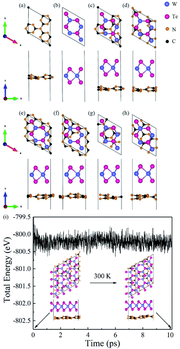
Firstly, we analyzed the geometry and electronic structures of monolayer g-C3N4 and WTe2. As shown in Fig. 1(a) and (b), g-C3N4 consists of N and C atoms in a staggered fashion similar to graphene with the optimized constant lattice of 6.95 Å, while monolayer WTe2 shows 2H phase with the optimized constant lattice of 3.52 Å, which agree well with previous works.46,47 We, therefore, built a g-C3N4/WTe2 heterostructure by stacking a 2 × 2 × 1 supercell of WTe2 upon the unit cell of g-C3N4 together with a lattice constant mismatch of 1.3%. Furthermore, we considered 6 possible stacking configurations by shifting g-C3N4 in a certain direction to explore the energetically favorable structure of the heterostructure, as illustrated in Fig. 1(c–h). Herein, the formation energy Eform was defined as
 | (1) |
 are the total energy of the g-C3N4/WTe2 heterostructure, freestanding g-C3N4 and WTe2 monolayer, respectively. On the other hand, the vdW binding energy Eb was defined as48
 | (2) |
| Configurations | I | II | III | IV | V | VI |
|---|---|---|---|---|---|---|
| a (Å) | 6.993 | 7.098 | 6.989 | 6.988 | 6.993 | 6.986 |
| dlayer (Å) | 3.076 | 3.653 | 3.312 | 3.111 | 3.177 | 3.325 |
| Ef (eV) | −0.652 | −0.117 | −0.645 | −0.640 | −0.604 | −0.634 |
| Eb (meV Å−2) | 15.81 | 15.33 | 15.79 | 14.35 | 13.46 | 15.07 |
To prove the thermodynamically stability, Born–Oppenheimer ab initio molecular dynamics (AIMD) simulations were adopted for the proposed g-C3N4/WTe2 heterostructure at 300 K for 10 ps. A 2 × 2 supercell has been constructed for the AIMD calculations. Fig. 1(i) displays the energy evolution and structure snapshots after 300 K annealing for 10 ps of the g-C3N4/WTe2 heterostructures. It is noted that the structure snapshots suggest that atoms just move near their equilibrium location during the simulations, and there is no structural reconstruction at 300 K. At the same time, the changes of the total energy are very small during the simulations from Fig. 1(i), indicating that the proposed g-C3N4/WTe2 vdW heterostructure is thermodynamically stability at 300 K.
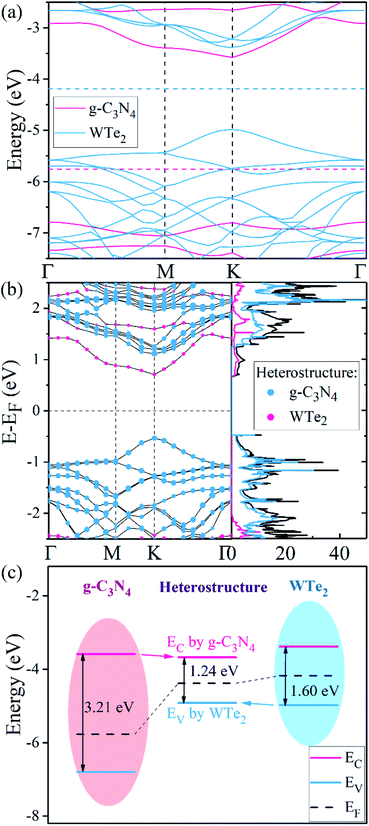
Fig. 2(a) shows the band structures of freestanding g-C3N4 and WTe2 monolayers using HSE06 calculations. To compare clearly, the vacuum level was set to 0 eV as a baseline. It can be found that g-C3N4 has an indirect band gap of 3.21 eV, where CBM and VBM locate at the K (1/3, 1/3, 0) and Γ (0, 0, 0) point, respectively. Meanwhile, the WTe2 shows the direct gap feature with the band gap of 1.60 eV, where both CBM and VBM locate at the K (1/3, 1/3, 0) point. These results agree well with the previously published studies.46,47 On the other hand, the projected band structure and partial density of states of g-C3N4/WTe2 heterostructure is plotted in Fig. 2(b), in which the projected weight of g-C3N4 and WTe2 are distinguished by size and color. The pink and blue balls represent the contributions from g-C3N4 and WTe2, respectively. For g-C3N4/WTe2 heterostructure, both CBM and VBM locate at the K (1/3, 1/3, 0) point, showing the direct band gap feature, with the calculated HSE06 band gap of 1.24 eV. Interestingly, the g-C3N4/WTe2 heterostructure shows the band structure feature of a type-II heterostructure,51 where CBM is contributed by the g-C3N4 layer and VBM is occupied by the WTe2 layer. The band alignment diagrams for isolated g-C3N4, WTe2 monolayer, and heterostructure interface are illustrated in Fig. 2(c). Obviously, the work function of the g-C3N4/WTe2 heterostructure lies between the g-C3N4 and WTe2 monolayers. When g-C3N4 and WTe2 come into contact, the electrons flow from WTe2 to g-C3N4 due to the lower work function of WTe2 and vice versa for the holes. As a result of the increased transfer of electrons, the Fermi level shifts and finally reaches the same energy level. The differences between the band structure of g-C3N4/WTe2 heterostructure and corresponding monolayers indicate that the vdW interactions play an essential role in the electronic structures.
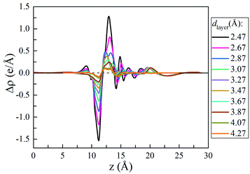
To understand the vdW interlayer interaction between the different parts of the heterostructure, we further investigated g-C3N4/WTe2 heterostructure with different interlayer distance dlayer of the vdW gap. As shown in Fig. 3, both Eform and −Eb follow the Lenard-Jones type relation as a function of dlayer,52 and a lower value of −Eb correspond to a stronger binding. Clearly, g-C3N4/WTe2 heterostructure with the equilibrium dlayer holds the most negative Eform and −Eb. As the dlayer decreases, both Eform and −Eb increase dramatically. As the dlayer increases, Eform and −Eb gradually increases towards zero. Herein, Eform and −Eb remain negative among an extensive range of dlayer, indicating the possibility to tune the interlayer interaction by varying dlayer. As mentioned before, there is the transfer of electrons within the vdW gap, which affects the electronic structure of the g-C3N4/WTe2 heterostructure. Thereby, we calculated the planar-averaged charge density differences of g-C3N4/WTe2 heterostructure with different dlayer, as shown in Fig. 4. Here, the plane-averaged electron density difference Δρ was calculated by
| Δρ = ρg-C3N4/WTe2 − ρg-C3N4 − ρWTe2 | (3) |
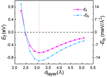 | ||
| Fig. 3 Formation energy Eform and binding energy −Eb as a function of interlayer distance dlayer of the vdW gap. | ||
To further explore the influence of the vdW interactions on the electronic structures of the g-C3N4/WTe2 heterostructure, we plotted the band gap, band alignment, and work function of g-C3N4/WTe2 heterostructure with different dlayer in Fig. 5(a). The PBE and HSE06 results show similar trends that the band gap decreases continuously as dlayer decreases. Oppositely, as dlayer increases, the band gap increases towards a balance value of 1.44 eV (HSE06). In addition, since the band alignment and work function are crucial in semiconductor heterostructure-based functional device designs, we plotted the band alignment and work function of the g-C3N4/WTe2 heterostructure corresponding to the vacuum level, as shown in Fig. 5(b). Correspondingly, the band alignment and work function show similar trends of band gap with different dlayer. As the dlayer decreases, CBM shifts downward continuously, and VBM shifts upward continuously, which reduces the band gap. On the contrary, as dlayer increases, CBM and VBM shift oppositely and towards convergent.
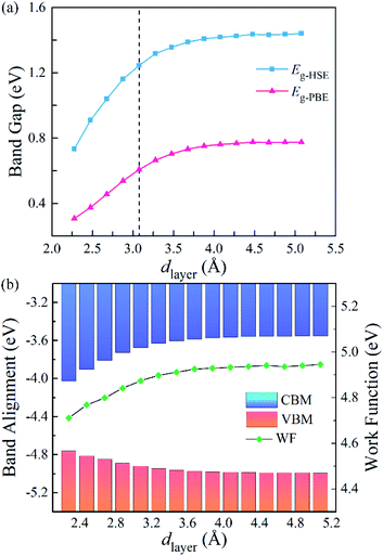 | ||
| Fig. 5 (a) Band gap, (b) band edge alignments and work function of g-C3N4/WTe2 heterostructure as a function of vdW gap. | ||
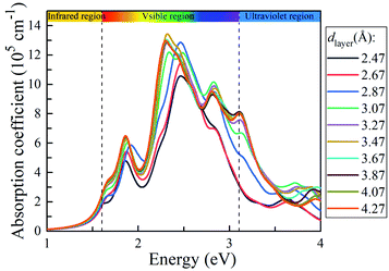
To explore the solar light-harvesting ability of the g-C3N4/WTe2 heterostructure, we calculated the optical absorption coefficients with a series of dlayer. As presented in Fig. 6, there are three absorption peaks in the visible light region for the equilibrium vdW gap dlayer = 3.07 Å. The first absorption peak locates at ∼1.9 eV, and the main peak covers the light energy region of 2.25–2.6 eV with an ultra-high light absorption coefficient up to 1.22 × 106 cm−1. And the third absorption peak locating at ∼2.8 eV presents the absorption coefficient of about ∼1 × 106 cm−1. It is worth noting that the light-harvesting ability in the entire visible solar spectrum is elevated when the dlayer increases. Interestingly, the absorption peaks shift weakly towards the lower energy region as the dlayer rises, and the absorption coefficient increases the maximum value up to 1.34 × 106 cm−1 when dlayer = 3.47 Å. Due to the direct band gap feature being beneficial for separating photo-excited electron–hole pairs and strong light absorption, the g-C3N4/WTe2 heterostructure could be a promising material for efficient photovoltaic solar cells and optoelectronic devices.
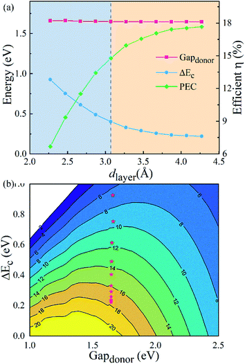
Furthermore, we estimated the power conversion efficiency (PCE) by the method proposed by Scharber et al.,53 which is widely used in efficiency estimation. The upper limited PCE of the g-C3N4/WTe2 heterostructure is described by54,55
 | (4) |
Conclusion
To conclude, based on the first-principle calculations, we have constructed the g-C3N4/WTe2 heterostructure and systematically analyzed the corresponding electronic band structure, optical properties with different dlayer. As the dlayer increases, the band gap rises from 1.24 to 1.44 eV when the interlayer interactions become weaker, which brings an augmented light harvest in the visible range. Significantly, the maximum optical absorption coefficient can reach ∼106 cm−1 level. Furthermore, the larger band gap and smaller band alignment difference make it better for light absorption and energy conversion. Finally, we found that the PCE of g-C3N4/WTe2 heterostructure has been promoted obviously during vdW gap tuning. The optimized PCE can reach up to 17.68%. Our results show that the g-C3N4/WTe2 heterostructure is favorable in solar cell applications. Here, we gave a tasteful way to realize the better performances of heterostructures, which is vital in the future study of vdW heterostructures.Conflicts of interest
The authors declare no competing financial interest.Acknowledgements
This work was supported by the National Natural Science Foundation of China (No. 21973012 and 51872049), the Natural Science Foundation of Fujian Province (Grant No. 2021J06011, 2020J01351, and 2020J01474), the Fujian Provincial Department of Science & Technology (2021H6011), and the “Qishan Scholar” Scientific Research Project of Fuzhou University.References
- K. S. Novoselov, A. K. Geim, S. V. Morozov, D. Jiang, Y. Zhang, S. V. Dubonos, I. V. Grigorieva and A. A. Firsov, Science, 2004, 306, 666–669 CrossRef CAS PubMed.
- C. Tan, X. Cao, X. J. Wu, Q. He, J. Yang, X. Zhang, J. Chen, W. Zhao, S. Han, G. H. Nam, M. Sindoro and H. Zhang, Chem. Rev., 2017, 117, 6225–6331 CrossRef CAS PubMed.
- C. Chang, W. Chen, Y. Chen, Y. Chen, Y. Chen, F. Ding, C. Fan, H. Jin Fan, Z. Fan, C. Gong, Y. Gong, Q. He, X. Hong, S. Hu, W. Hu, W. Huang, Y. Huang, W. Ji, D. Li, L.-J. Li, Q. Li, L. Lin, C. Ling, M. Liu, N. Liu, Z. Liu, K. Ping Loh, J. Ma, F. Miao, H. Peng, M. Shao, L. Song, S. Su, S. Sun, C. Tan, Z. Tang, D. Wang, H. Wang, J. Wang, X. Wang, X. Wang, A. T. S. Wee, Z. Wei, Y. Wu, Z.-S. Wu, J. Xiong, Q. Xiong, W. Xu, P. Yin, H. Zeng, Z. Zeng, T. Zhai, H. Zhang, H. Zhang, Q. Zhang, T. Zhang, X. Zhang, L.-D. Zhao, M. Zhao, W. Zhao, Y. Zhao, K.-G. Zhou, X. Zhou, Y. Zhou, H. Zhu, H. Zhang and Z. Liu, Acta Phys.-Chim. Sin., 2021, 37, 2108017 Search PubMed.
- X. Li and L. Zhi, Chem. Soc. Rev., 2018, 47, 3189–3216 RSC.
- I. V. Lightcap and P. V. Kamat, Acc. Chem. Res., 2012, 46, 2235–2243 CrossRef PubMed.
- Y. T. Du, X. Kan, F. Yang, L. Y. Gan and U. Schwingenschlogl, ACS Appl. Mater. Interfaces, 2018, 10, 32867–32873 CrossRef CAS PubMed.
- B. Anasori, M. R. Lukatskaya and Y. Gogotsi, Nat. Rev. Mater., 2017, 2, 16098 CrossRef CAS.
- R. Li, Y. Cheng and W. Huang, Small, 2018, 14, 1802091 CrossRef PubMed.
- Y. Wang, Y. Xu, M. Hu, H. Ling and X. Zhu, Nanophotonics, 2020, 9, 1601–1620 CrossRef CAS.
- C. Liu, H. Chen, S. Wang, Q. Liu, Y. G. Jiang, D. W. Zhang, M. Liu and P. Zhou, Nat. Nanotechnol., 2020, 15, 545–557 CrossRef CAS PubMed.
- J. Chen, S. Cai, R. Xiong, B. Sa, C. Wen, B. Wu and Z. Sun, Phys. Chem. Chem. Phys., 2020, 22, 7039–7047 RSC.
- Y. Zhu, L. Gong, D. Zhang, X. Wang, J. Zhang, L. Zhang, L. Dai and Z. Xia, Nano Energy, 2019, 63, 103819 CrossRef CAS.
- G. P. Gao, A. P. O'Mullane and A. J. Du, ACS Catal., 2017, 7, 494–500 CrossRef CAS.
- Q. Peng, Z. Wang, B. Sa, B. Wu and Z. Sun, ACS Appl. Mater. Interfaces, 2016, 8, 13449–13457 CrossRef CAS PubMed.
- S. J. Kang, D. H. Lee, J. Kim, A. Capasso, H. S. Kang, J. W. Park, C. H. Lee and G. H. Lee, 2D Materials, 2020, 7, 022003 CrossRef CAS.
- L. Ju, M. Bie, X. Tang, J. Shang and L. Kou, ACS Appl. Mater. Interfaces, 2020, 12, 29335–29343 CAS.
- S. Arra, R. Babar and M. Kabir, Phys. Rev. Mater., 2019, 3, 095402 CrossRef CAS.
- X. Huang, Z. Zeng and H. Zhang, Chem. Soc. Rev., 2013, 42, 1934–1946 RSC.
- S. Manzeli, D. Ovchinnikov, D. Pasquier, O. V. Yazyev and A. Kis, Nat. Rev. Mater., 2017, 2, 17033 CrossRef CAS.
- C. K. Sumesh, Sol. Energy Mater. Sol. Cells, 2019, 192, 16–23 CrossRef CAS.
- J. Fu, J. Yu, C. Jiang and B. Cheng, Adv. Energy Mater., 2018, 8, 1701503 CrossRef.
- G. Mamba and A. K. Mishra, Appl. Catal., B, 2016, 198, 347–377 CrossRef CAS.
- S. Cao and J. Yu, J. Phys. Chem. Lett., 2014, 5, 2101–2107 CrossRef CAS PubMed.
- J. Wen, J. Xie, X. Chen and X. Li, Appl. Surf. Sci., 2017, 391, 72–123 CrossRef CAS.
- M. D. Hernandez-Alonso, F. Fresno, S. Suarez and J. M. Coronado, Energy Environ. Sci., 2009, 2, 1231–1257 RSC.
- Y. H. Li, M. L. Gu, X. M. Zhang, J. J. Fan, K. L. Lv, S. A. C. Carabineiro and F. Dong, Mater. Today, 2020, 41, 270–303 CrossRef CAS.
- P. Niu, L. L. Zhang, G. Liu and H. M. Cheng, Adv. Funct. Mater., 2012, 22, 4763–4770 CrossRef CAS.
- X. H. Niu, Y. H. Li, Y. H. Zhang, Q. J. Zheng, J. Zhao and J. L. Wang, J. Mater. Chem. C, 2019, 7, 1864–1870 RSC.
- A. K. Geim and I. V. Grigorieva, Nature, 2013, 499, 419–425 CrossRef CAS PubMed.
- Q. Wang, J. Li, Y. Liang, B. Wang and Y. Nie, J. Mater. Chem. A, 2019, 7, 10684–10695 RSC.
- X. H. Yang, B. S. Sa, P. Lin, C. Xu, Q. Zhu, H. B. Zhan and Z. M. Sun, J. Phys. Chem. C, 2020, 124, 23699–23706 CrossRef CAS.
- S. Y. Xie, H. Jin, J. W. Li and Y. D. Wei, ACS Appl. Electron. Mater., 2021, 3, 898–904 CrossRef CAS.
- M. M. Furchi, A. Pospischil, F. Libisch, J. Burgdorfer and T. Mueller, Nano Lett., 2014, 14, 4785–4791 CrossRef CAS PubMed.
- C. Li, Q. Cao, F. Wang, Y. Xiao, Y. Li, J. J. Delaunay and H. Zhu, Chem. Soc. Rev., 2018, 47, 4981–5037 RSC.
- Q. Peng, Z. Wang, B. Sa, B. Wu and Z. Sun, Sci. Rep., 2016, 6, 31994 CrossRef CAS PubMed.
- L. Xu, J. Zeng, Q. Li, T. Chen, K.-W. Luo, X. Luo, B. Peng, Z. Ma, L.-L. Wang, X. Zhu, S. Huang, D. Liu, S. X. Xiong and C. Shuai, Appl. Surf. Sci., 2020, 530, 147181 CrossRef CAS.
- B. Li, H. Song, F. Han and L. Wei, Appl. Catal., B, 2020, 269, 118845 CrossRef CAS.
- J. L. Silva, B. Brena and C. M. Araujo, J. Phys. Chem. C, 2020, 124, 8726–8735 CrossRef CAS.
- G. J. Wang, L. Y. Peng, K. Q. Li, L. G. Zhu, J. Zhou, N. H. Miao and Z. M. Sun, Comput. Mater. Sci., 2021, 186, 110064 CrossRef CAS.
- J. Hafner, J. Comput. Chem., 2008, 29, 2044–2078 CrossRef CAS PubMed.
- J. P. Perdew and Y. Wang, Phys. Rev. B, 1992, 45, 13244–13249 CrossRef PubMed.
- G. Kresse and J. Hafner, Phys. Rev. B, 1993, 48, 13115–13118 CrossRef CAS PubMed.
- J. P. Perdew, K. Burke and Y. Wang, Phys. Rev. B, 1996, 54, 16533–16539 CrossRef CAS PubMed.
- S. Grimme, J. Antony, S. Ehrlich and H. Krieg, J. Chem. Phys., 2010, 132, 154104 CrossRef PubMed.
- J. Paier, M. Marsman, K. Hummer, G. Kresse, I. C. Gerber and J. G. Angyan, J. Chem. Phys., 2006, 124, 154709 CrossRef CAS PubMed.
- H. H. Huang, X. Fan, D. J. Singh, H. Chen, Q. Jiang and W. T. Zheng, Phys. Chem. Chem. Phys., 2016, 18, 4086–4094 RSC.
- Q. Gao, S. Hu, Y. Du and Z. Hu, J. Mater. Chem. A, 2017, 5, 4827–4834 RSC.
- Z. Ma, R. Li, R. Xiong, Y. Zhang, C. Xu, C. Wen and B. Sa, Materials, 2021, 14, 3768 CrossRef CAS PubMed.
- T. Bjorkman, A. Gulans, A. V. Krasheninnikov and R. M. Nieminen, Phys. Rev. Lett., 2012, 108, 235502 CrossRef CAS PubMed.
- J. Chen, X. He, B. Sa, J. Zhou, C. Xu, C. Wen and Z. Sun, Nanoscale, 2019, 11, 6431–6444 RSC.
- R. Xiong, R. Hu, Y. Zhang, X. Yang, P. Lin, C. Wen, B. Sa and Z. Sun, Phys. Chem. Chem. Phys., 2021, 23, 20163–20173 RSC.
- B. Sa, N. Miao, J. Zhou, Z. Sun and R. Ahuja, Phys. Chem. Chem. Phys., 2010, 12, 1585–1588 RSC.
- M. C. Scharber, D. Mühlbacher, M. Koppe, P. Denk, C. Waldauf, A. J. Heeger and C. J. Brabec, Adv. Mater., 2006, 18, 789–794 CrossRef CAS.
- M. Bernardi, M. Palummo and J. C. Grossman, ACS Nano, 2012, 6, 10082–10089 CrossRef CAS PubMed.
- J. Dai and X. C. Zeng, J. Phys. Chem. Lett., 2014, 5, 1289–1293 CrossRef CAS PubMed.
| This journal is © The Royal Society of Chemistry 2022 |

