
 Open Access Article
 This Open Access Article is licensed under a Creative Commons Attribution-Non Commercial 3.0 Unported Licence
NiCo2O4 thin film prepared by electrochemical deposition as a hole-transport layer for efficient inverted perovskite solar cells†
Sen Wanga,
Linqin Wangb,
Chang Liua,
Yu Shana,
Fusheng Li *a and
Licheng Sunab
*a and
Licheng Sunab
aState Key Laboratory of Fine Chemicals, Institute of Artificial Photosynthesis, DUT-KTH Joint Education and Research Centre on Molecular Devices, Dalian University of Technology, Dalian, 116024, P. R. China. E-mail: fusheng@dlut.edu.cn
bCenter of Artificial Photosynthesis for Solar Fuels, School of Science, Westlake University, 310024, Hangzhou, China
First published on 26th April 2022
Abstract
Spinel NiCo2O4 is a promising p-type semiconductor for optoelectronic devices; however, it is difficult to prepare uniform and large-area NiCo2O4 films, which hinders its application as a hole transport material for perovskite solar cells (PSCs). In this study, a novel, mild, and low-cost KCl-assisted electrochemical deposition (ECD) approach was developed to directly prepare a uniform NiCo2O4 film on a fluorine-doped tin oxide (FTO) substrate. A uniform NiCo2O4 film prepared through an ECD approach was used as a hole-transport layer (HTL) in inverted PSCs. The resulting NiCo2O4 HTL-based device achieved a power conversion efficiency (PCE) of 19.24% with negligible hysteresis and excellent reproducibility. Additionally, it outperformed a NiOx-based device (PCE = 18.68%). The unsealed devices retained 90.7% of their initial efficiency when subjected to stability measurements for 360 h in an ambient atmosphere. This study shows the great potential of ECD-prepared NiCo2O4 HTLs for large-area PSCs in the future.
Introduction
Recently, organic-inorganic hybrid perovskite solar cells (PSCs) have attracted tremendous attention owing to their low cost and high power conversion efficiency (PCE).1–4 In a typical PSC structure, carrier-transport layers (CTLs) connected with perovskite materials could not only improve the charge transfer from the perovskite light absorption layer to the current-collecting electrode, but also block the injection of the opposite charge carrier.5,6 Meanwhile, the CTL can also act as a protective layer to prevent perovskite from exposure to water and oxygen. Therefore, a suitable CTL is crucial to improve the PCE and stability of PSCs.7Numerous materials have been used as hole-transport layers (HTLs) for PSCs. However, most of the popular hole-transport materials (HTMs) used in conventional n-i-p type PSCs, such as 2,2,7,7-tetrakis(N,N-di-p-methoxyphenyl-amino)-9,9-spirobifluorene (spiro-OMeTAD), polytriarylamine (PTAA), and other molecules, are poor conductors which require extra chemical doping to offset their insufficient mobility and conductivity.8,9 This decreases the stability and increases costs, thereby hindering the commercial application of these materials as HTLs in PSCs. In inverted-structured PSCs, poly(3,4-ethylenedioxythiophene):poly(styrenesulfonate) (PEDOT:PSS) is frequently employed as an organic HTL. PEDOT:PSS demonstrates excellent electrical conductivity and moderate processing, but its acidic, hydrophilic nature induces the degradation of the perovskite component and sequentially restricts its development as a superior HTL in solar cells.10 Generally, inorganic HTMs are low-cost and exhibit better physical and chemical stability than that of organic materials. Besides, they also have tunable optical and electrical properties, which made them promising HTLs.11 Among them, NiOx materials are one of the most commonly used inorganic HTMs in inverted PSCs. However, they have relatively low intrinsic conductivity, which needs to be addressed prior to their application.12–14 Ternary oxides are ideal replacements for NiOx because of their respectable hole extraction and transporting abilities, good conductivity, and tunable optical properties. Early in 2016, Liao and Wang et al. reported a CuAlO2 material prepared by magnetron sputtering method, which was employed as hole selective buffer layer in inverted planer PSCs and achieved a PCE of 14.5%.15 Later, solution-processed CuGaO2 nanoplates were synthesized by a microwave-assisted hydrothermal method by Jen and Chen et al., and the CuGaO2 nanoplates were used as HTL in the n-i-p configuration PSCs with a promising PCE of 18.5% and improved ambient stability.16 Furthermore, a CuyCrzO2 HTL synthesized by the sol–gel method was reported by Fang and Li et al., and the resulting PSCs achieved a high PCE of 17.19% on glass and 15.53% on flexible PET substrates, which were much higher than mono-metal oxide-based devices.17
NiCo2O4 is a p-type semiconductor with a cubic spinel structure, in which Ni ions occupy the octahedral sites while Co ions are distributed across both octahedral and tetrahedral sites.18 NiCo2O4 has the advantages of being abundant, relatively inexpensive, and environmentally friendly, making it a promising candidate for future commercialization. These properties are desirable for the use of NiCo2O4 in various electronic devices, such as supercapacitors,18 lithium-ion batteries,19 electrocatalysts for water splitting,20 etc. Besides, NiCo2O4 has the highest conductivity (500 S cm−1) among transparent conducting oxides, which is much higher compared to a NiOx-based HTL.21,22 Additionally, NiCo2O4 possesses a wide optical bandgap and a deep valence band position, which matches well with the valence band (VB) of perovskite material, especially for CH3NH3PbI3 (MAPbI3).23
In 2018, Choy et al. synthesized well-dispersed NiCo2O4 nanoparticles (NPs) through a controllable Co–NH3 deamination reaction in a sol system containing Ni(OH)2 and the resulting inverted-structured PSC based on this NiCo2O4 HTL yielded a PCE of 18.23% and exhibited high stability.24 Same year, Choulis et al. applied combustion-synthesized ultrasmall NiCo2O4 NPs as HTL to form inverted-structure PSCs and achieved a PCE of 15.5%.25 Recently, Jung et al. reported the conventional-structured PSCs fabricated with featured HTLs comprising sol–gel-driven NiCo2O4 and yielded PCEs of up to 18.16%.23 Akhter et al. used NiCo2O4 NPs synthesized via a chemical co-precipitation method as HTLs in n-i-p type PSCs and achieved a PCE of >14%.26 These work not only demonstrated that ternary oxide NiCo2O4 could be used as an HTL in PSCs, but also suggested a possible way to synthesize ultrasmall NPs even though the preparation methods for ultrafine NiCo2O4 NPs are energetically demanding, expensive, and time-consuming. Meanwhile, the above researches show that the spin-coating process is the most commonly adopted strategy for fabricating NiCo2O4 HTLs, but this method can be relatively inefficient regarding the reduction in the waste of materials. Therefore, an easy, low-cost, and controllable method for preparing compact and uniform NiCo2O4 HTLs is urgently needed.
As a mature and completely commercialized technology, electrochemical deposition (ECD) is often utilized to prepare nanomaterials on different conductive substrates. Owing to its low cost, low-temperature requirements, large-area production, and precise control, it can be controlled by regulating the deposition time, current, and/or voltage.27–31 To ensure a good conductivity of the precursor solution, potassium chloride (KCl) is commonly introduced as a supporting electrolyte.32 In addition, because of the strong adsorption behavior of Cl−,33,34 KCl may play an additional role in the nanomaterials formation process via ECD technique. In this study, NiCo2O4 films were prepared via a KCl-assisted ECD process to construct HTLs for the first time for MAPbI3-based inverted-structure PSCs (Scheme 1). The aim of this study was to explore the potential of ECD-prepared NiCo2O4 HTLs for PSCs, and to provide a new perspective on the preparation of advanced HTLs for further enhancement of the PCEs of PSCs via ECD methods.
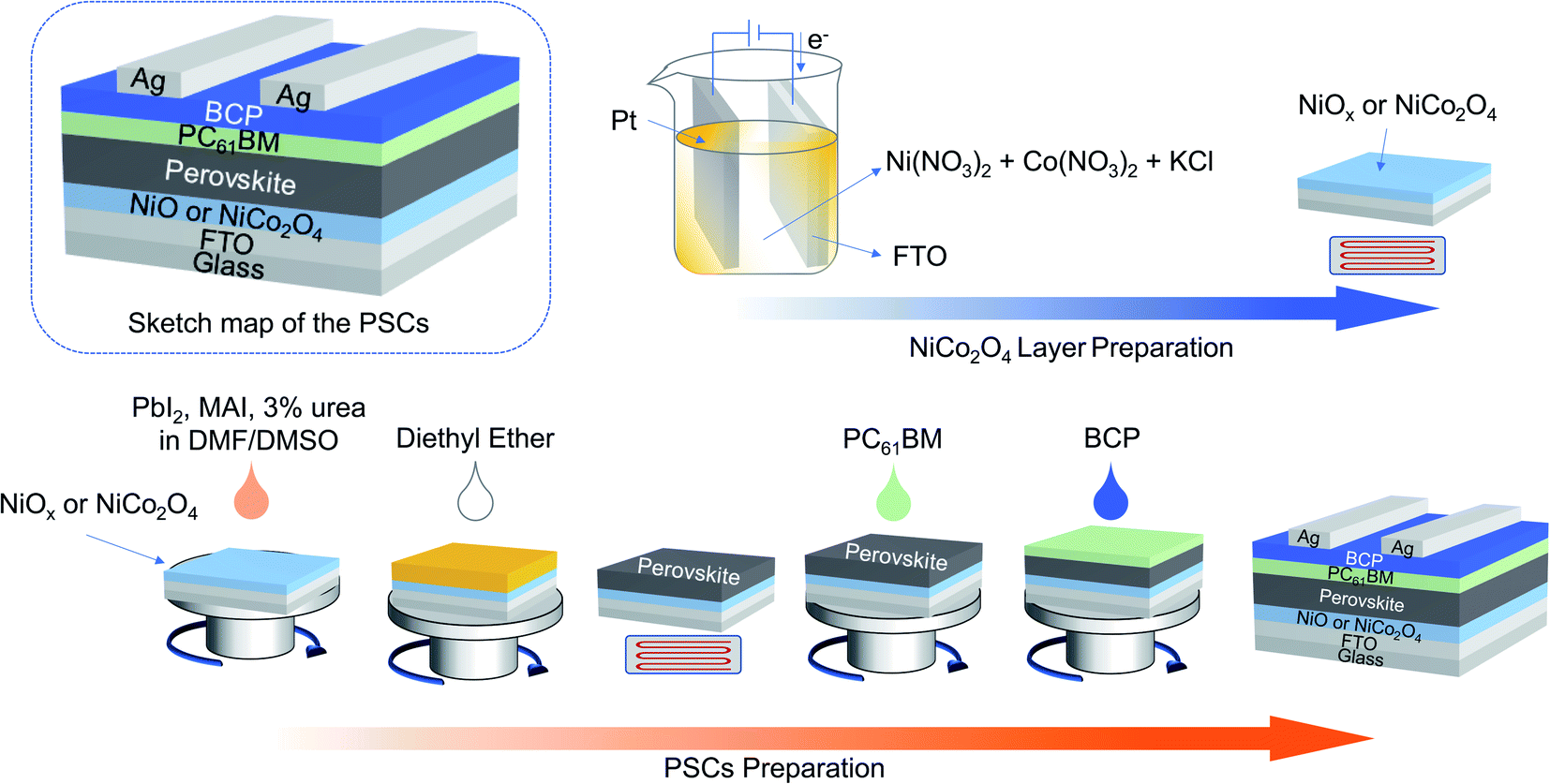 | ||
| Scheme 1 Schematic illustrations of NiCo2O4 film fabrication process, prepared via electrochemical deposition, and of perovskite solar cell (PSC) preparation procedure. FTO: fluorine-doped tin oxide, DMF: dimethylformamide, DMSO: dimethyl sulfoxide. | ||
Experimental
Synthesis of NiCo2O4 and NiOx films
Patterned fluorine-doped tin oxide (FTO)/glass substrates were successively cleaned in a detergent solution, deionized water, acetone, and isopropanol for 30 min with ultrasonic treatment, respectively. Before using, all substrates were treated with ultraviolet ozone for 20 min. The ECD processes for NiCo2O4 or NiOx were carried out with a three-electrode system, where the cleaned FTO glass functioned as the working electrode, a Pt foil was used as the counter electrode, and the reference electrode comprised saturated Ag/AgCl. Three kinds of electrolytes containing 20 mM Co(NO3)2·6H2O, 10 mM Ni(NO3)2·6H2O and different concentrations of KCl (0, 50, and 100 mM) were used, thus the stoichiometric Ni![[thin space (1/6-em)]](https://www.rsc.org/images/entities/char_2009.gif) :Co:K ratios for these different electrolytes were 1:2:0, 1:2:5, and 1:2:10, respectively. After the NiCo2O4 precursors were deposited on the surface of each FTO glass substrate, the films were annealed in a furnace at 300 °C for 2 h in air. The resulting samples are denoted herein as NiCo2O4 (0-NiCo2O4, 5-NiCo2O4, and 10-NiCo2O4, respectively). For comparison, 30 mM Ni(NO3)2 in water was selected as the deposition solution for the preparation of NiOx. The ECD process was carried out by a chronopotentiometry method with a current density of 0.3 mA cm−2. The as-deposited film was then rinsed with deionized water before being annealed in a tube furnace at 300 °C for 1 h.
:Co:K ratios for these different electrolytes were 1:2:0, 1:2:5, and 1:2:10, respectively. After the NiCo2O4 precursors were deposited on the surface of each FTO glass substrate, the films were annealed in a furnace at 300 °C for 2 h in air. The resulting samples are denoted herein as NiCo2O4 (0-NiCo2O4, 5-NiCo2O4, and 10-NiCo2O4, respectively). For comparison, 30 mM Ni(NO3)2 in water was selected as the deposition solution for the preparation of NiOx. The ECD process was carried out by a chronopotentiometry method with a current density of 0.3 mA cm−2. The as-deposited film was then rinsed with deionized water before being annealed in a tube furnace at 300 °C for 1 h.
Device fabrication
PbI2 (461 mg) and CH3NH3I (MAI, 159 mg) were first dissolved in anhydrous dimethylformamide (DMF, 634 μL) and anhydrous dimethyl sulfoxide (DMSO, 70.9 μL), respectively. Then, 3 mol% urea (versus PbI2 or MAI) was added to the solution, and the mixture was then magnetically stirred for 3 h at room temperature in a nitrogen-filled glovebox. The NiCo2O4 and NiOx films were then transported to the glovebox for the preparation of perovskite films, which was conducted through a one-step antisolvent-assisted procedure.35 The precursor solution was spin-coated onto NiOx or NiCo2O4 coated FTO at 1000 rpm for 10 s, and 4000 rpm for 30 s in sequence. Then, 200 μL diethyl ether was quickly dripped onto the film at the high-speed step. The resulting film was heated at 65 °C for 1 min, and then at 100 °C for 10 min. Subsequently, a layer of [6,6]-phenyl-C61-butyric acid methyl ester (PC61BM; 20 mg mL−1 in chlorobenzene) was spin-coated onto the perovskite layer at 1500 rpm for 30 s, following which a thin layer of bathocuproine (BCP; 0.5 mg mL−1 in isopropanol) was deposited on top of the PC61BM layer at 5000 rpm for 30 s. Finally, Ag film with 100 nm thickness was thermally evaporated under vacuum (<5 × 10⁻⁴ Pa) to form the contact electrode.Characterizations
The J–V curves of the prepared devices were measured under standard 1 sun, AM 1.5 G conditions, with a solar simulator (Newport 94023A, USA), with 0.1 V s−1. The electrochemical impedance spectroscopy (EIS) was performed in the dark at a potential of 1.0 V, the frequency was swept from 0.1 Hz to 1 MHz using an electrochemical workstation (Zennium X, Zahner), and the oscillation potential amplitude was adjusted to 10 mV. The crystal structure of NiOx or NiCo2O4 film was by X-ray diffraction (XRD, 9 kW, SmartLab). The elemental composition and the energy level of NiCo2O4 film were characterized by X-ray photoelectron spectroscopy (XPS, ESCALAB XI+, Thermo Fisher Scientific) and ultraviolet photoelectron spectroscopy (UPS) with a monochromatic He–I light source with an incident energy of 21.22 eV. The morphology of samples was examined by scanning electron microscopy (SEM, SU8220, Hitachi). Optical transmission spectroscopy of NiOx or NiCo2O4 film were collected by UV-visible spectrophotometer (Agilent 8453). The electrical performance of NiOx or NiCo2O4 film was analyzed by a Hall-effect system (8400, Lake Shore).Results and discussion
As shown in Scheme 1, the NiCo2O4 precursor was prepared by chronopotentiometry with a current density of 0.3 mA cm−2 for a range of different times. In the inverted-structured PSCs, the perovskite layer based on the as-prepared NiCo2O4 HTLs was constructed by a one-step antisolvent-assisted procedure, in which a spin-coated PC61BM layer was used as the ETL and Ag was used as the counter electrode.XRD was used to characterize the crystal structures of the NiCo2O4 series films on each FTO/glass substrate. As shown in Fig. 1a, the diffraction peaks of the FTO/glass substrate could be detected in all of the XRD patterns of the samples, owing to the ultrathin thickness of the electrodeposited films. In addition to the strong base peaks, three weak diffraction peaks located at 18.9°, 31.1°, and 36.6° were observed, which could be assigned as (111), (220), and (311) crystal planes respectively of the standard patterns of the cubic spinel NiCo2O4 crystalline phase (JCPDF#73-1072). The XRD results demonstrated that well-crystallized NiCo2O4 films were obtained via ECD method with/without KCl additive.
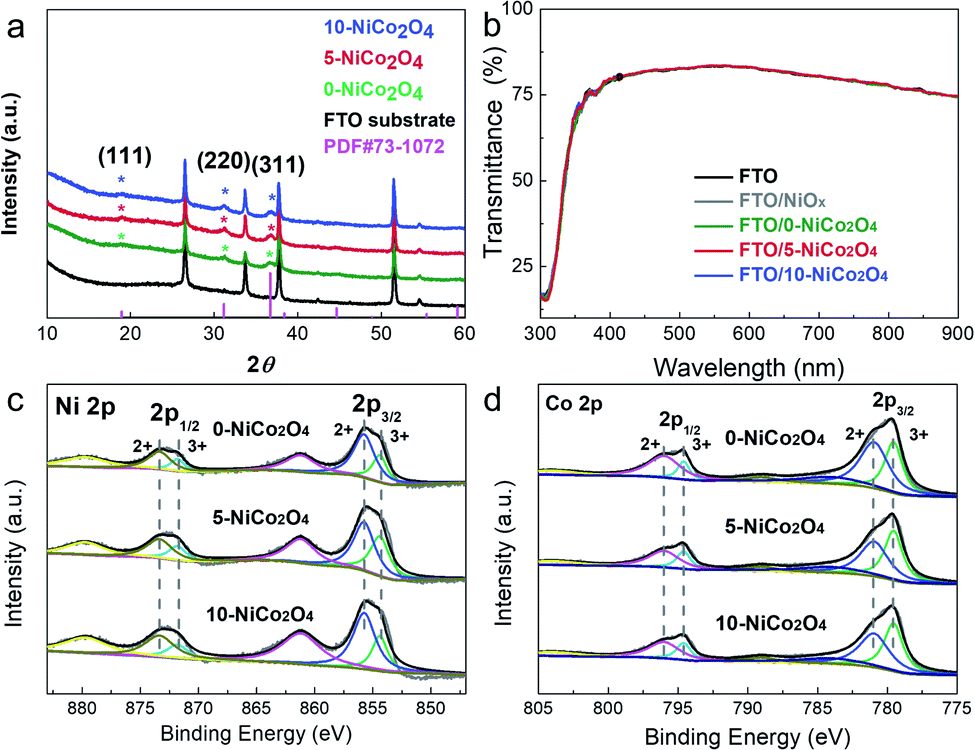 | ||
| Fig. 1 (a) XRD patterns of NiCo2O4 films deposited on FTO/glass substrates, (b) optical transmission spectra of NiOx and different NiCo2O4 films, and XPS spectra of (c) Ni 2p and (d) Co 2p for the NiCo2O4 films. | ||
Optical transmission spectra were conducted to characterize the optical properties of prepared NiOx and NiCo2O4 films deposited on the FTO/glass substrate. As shown in Fig. 1b, all samples exhibited almost the same transmission properties as the bare FTO/glass substrate, which maintained a high transmittance (>75% across the spectral range of 400–850 nm). The high transparency of the prepared HTLs minimized the optical losses of the photovoltaic devices and exhibited no competition with the light absorption layer perovskite, thereby ensuring considerable photon-generated carriers. In addition, the optical bandgap of the NiCo2O4 material was estimated to be 1.88 eV from the Tauc plot (Fig. S1†), which is slightly lower than the previously reported value for NiCo2O4 NPs.24
To further analyze the elemental composition and chemical bonding states of NiCo2O4 films, XPS measurements were performed. The high-resolution XPS Ni 2p spectrum could be fitted to two spin–orbit doublets and two shakeup satellites (Fig. 1c). The well-fitted peaks at 855.8 eV (2p3/2) and 873.4 eV (2p1/2) were attributed to the characteristic peaks of the Ni2+ oxidation state, and the binding energies of 854.4 eV and 871.8 eV were indexed to Ni3+.24 According to this, the ratio of Ni3+/Ni2+ for 0-NiCo2O4, 5-NiCo2O4 and 10-NiCo2O4 was 0.43, 0.66, and 0.44, respectively, suggesting that optimized KCl additive concentration in deposition precursors was beneficial for the presence of Ni3+ state. Additionally, the presence of the Ni3+ state could have induced oxygen deficiency in the lattices, and further facilitated the generation of holes in the materials.23 Besides, the relatively high Ni3+/Ni2+ ratios on the surfaces of the NiCo2O4 films rendered a p-type semiconducting property to the material and increased conductivity, thereby promoting more efficient charge separation and transport.36,37 For Co 2p, the binding energies of 796.0 eV and 781.0 eV were indexed to Co2+, while the peaks of 794.6 eV and 779.5 eV were associated with Co3+ (Fig. 1d). The obtained binding energies of Ni 2p and Co 2p were consistent with previously reported values,24,38 and no differences were found between the 0-NiCo2O4, 5-NiCo2O4, and 10-NiCo2O4 films.
The morphologies of the NiOx and NiCo2O4 films were investigated through SEM characterization. As shown in Fig. 2a, the as-formed NiOx film had an extremely tiny fluffy porous structure and fully covered the FTO substrate. However, the 0-NiCo2O4 film had a messy porous structure with numerous intersecting nanosheets (Fig. 2b), resulting in plenty of pinholes and open space sites in the HTL films, which could not ensure complete contact at the HTL/perovskite interface.
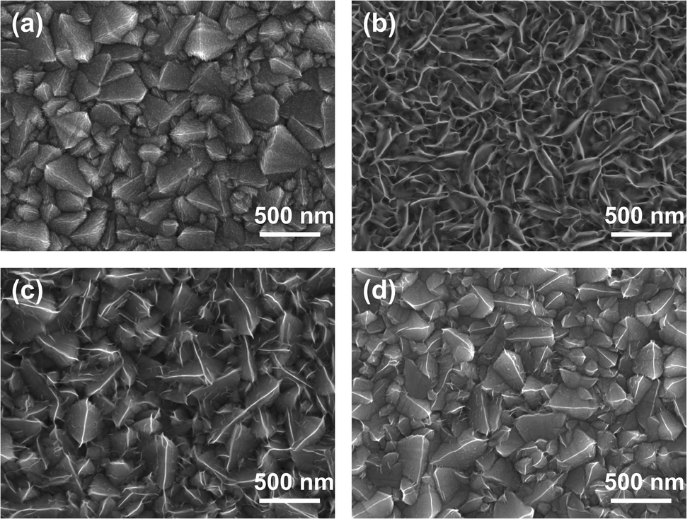 | ||
| Fig. 2 Top-view SEM images of (a) NiOx film, and (b) 0-NiCo2O4, (c) 5-NiCo2O4, and (d) 10-NiCo2O4 films deposited on FTO substrates. | ||
Fig. 2c and d illustrate the influence of the KCl additives on the surface morphology of the NiCo2O4 films. When KCl was added to the deposition solutions, the NiCo2O4 layers retained their pristine surface morphology covered on the FTO/glass substrates, which is beneficial for the adhesion of perovskite materials on the HTLs. And on this basis, the film quality of the resulting 5-NiCo2O4 films has been obviously improved, such as larger grain size and better coverage as well as improved compact nanocrystals quality in comparison with NiOx film (Fig. 2d). These improvements could be mainly attributed to the assistance of KCl in the previous report,33 which could further promote interface charge extraction and separation.
UPS measurements were performed to investigate the energy levels of the as-prepared NiCo2O4 films. Relative to the vacuum level, UPS revealed the valence band maximum (VBM) levels to be −4.99 eV, −4.94 eV and −4.79 eV for 0-NiCo2O4, 5-NiCo2O4 and 10-NiCo2O4, respectively (Fig. S2†). The corresponding energy diagram of a PSC based on the prepared NiCo2O4 HTL is illustrated in Fig. 3a. The VBM levels of samples 0-NiCo2O4 and 5-NiCo2O4 were clearly closer to that of MAPbI3 (−5.4 eV), indicating that their energy level matched with that of MAPbI3 very well when acting as HTLs, and would thus ensure efficient hole extraction at the corresponding interfaces. Furthermore, the electrical properties of the NiOx and NiCo2O4 layers were evaluated by Hall-effect measurements (Fig. 3b). The electrical conductivity and hole mobility of the NiCo2O4 films was almost two orders of magnitude higher than those of the NiOx film, demonstrating the superior charge transport properties of the NiCo2O4 films. Notably, the 5-NiCo2O4 film possessed the highest conductivity and hole mobility among all the NiCo2O4 films. The observed differences in VBM levels and electrical properties of NiCo2O4 may be attributed to the highest ratio of self-doping created by introducing most Ni3+ into the NiCo2O4 crystal lattice via appropriate KCl concentration,12,39 as discussed in the XPS analysis above.
 | ||
| Fig. 3 (a) Energy band diagram relative to a vacuum level of the device. (BCP: bathocuproine) (b) Hall-effect measurements of NiOx and NiCo2O4 films. (c) Steady-state photoluminescence of MAPbI3 based on NiOx and NiCo2O4 films. (d) Time-resolved photoluminescence spectra of the perovskite films on NiOx and NiCo2O4 HTLs. | ||
As shown in Fig. S3,† all of the perovskite films based on the NiOx and NiCo2O4 layers exhibited identical crystal structures and similar crystallinities. The main diffraction peaks at 14.16°, 28.78°, and 31.92° corresponded to the (110), (220), and (310) crystal planes of the perovskite (MAPbI3), respectively. No impurity peaks were observed, except for one weak peak located at 12.6° which was indexed to traces of excess PbI2. The strongest peak intensity of perovskite/5-NiCo2O4 suggested the best perovskite crystallinity on the 5-NiCo2O4 layer, while a similar phenomenon could be convinced by the top-view SEM images as shown in Fig. S4.† Less and smaller cracks appear in the NiCo2O4 supported perovskite layer. Especially for the perovskite/5-NiCo2O4 film, smooth and dense film morphologies were displayed with full surface coverage. These comparably high-quality films could directly influence solar cell performance. It can be seen from the UV-vis spectroscopy that the perovskite films based on NiOx and different NiCo2O4 HTLs exhibit similar absorption over the entire visible region (Fig. S5†).
The charge transfer dynamics of perovskite films deposited on NiOx or NiCo2O4 were studied via steady-state photoluminescence (PL) and time-resolved photoluminescence (TRPL) measurements with excitation at 550 nm. As shown in Fig. 3c, the highest PL intensity was observed for the bare MAPbI3 film. After the introduction of the HTLs, the PL intensity decreased drastically, following the order of: MAPbI3/10-NiCo2O4 > MAPbI3/NiOx > MAPbI3/0-NiCo2O4 > MAPbI3/5-NiCo2O4. MAPbI3/5-NiCo2O4 exhibited the highest degree of PL quenching, which means it achieved the best hole extraction and transport efficiency from perovskite to the HTL. This finding agrees well with its suitable energy level alignment and outstanding electrical properties, as discussed above. Fig. 3d shows the TRPL spectra of MAPbI3 films deposited on different HTLs. The PL decay curves have been fitted using a bi-exponential decay function as following eqn (1) and the corresponding parameters are summarized in Table S1.†
|
f (t) = A1exp(−t/τ) + A2exp(−t/τ) + B
| (1) |
To probe the effect of NiCo2O4 film as HTL on device performance, we firstly fabricated the inverted-structure PSCs (FTO/NiCo2O4/MAPbI3/PC61BM/BCP/Ag) with different thicknesses of 0-NiCo2O4 film (different deposition charge density) by a one-step antisolvent-assisted procedure. Fig. S6a† shows the J–V characteristic curves for the respective champion device, and the corresponding device parameters are summarized in Table S2.† Obviously, with the increase of deposition charge density for NiCo2O4 film, the device performance presented a tendency to increase first and then decrease. The thinner NiCo2O4 layer-based PSC (5 mC cm−2) displayed a inferior performance with a low current density. This can be attributed to the current leakage resulting from incomplete coverage of NiCo2O4 on FTO substrate. Meanwhile, the thicker NiCo2O4 layer-based PSC (20 mC cm−2) was also subjected to a poor current density due to the increase of series resistance (Rs). And the optimum thickness of NiCo2O4 layer was found to be a charge density of 10 mC cm−2, which resulted in a PCE of 18.66% with Jsc of 22.93 mA cm−2, Voc of 1.02 V, and fill factor (FF) of 0.78. The results were further confirmed by the efficiency distributions as a function of deposition charge density, as shown in Fig. S6b.†
We further fabricated the inverted PSCs based on NiOx and different NiCo2O4 HTLs at the charge density of 10 mC cm−2, the J–V characteristic curves of the respective champion devices are shown in Fig. 4a, and the corresponding photovoltaic parameters are summarized in Table 1. The J–V curves of champion devices based on NiOx and 0-NiCo2O4 HTLs almost overlapped. Among all the devices, the 5-NiCo2O4 HTL-based device displayed the highest PCE of 19.24%, a short-circuit current density (Jsc) of 24.31 mA cm−2, a fill factor (FF) of 0.78, and an open-circuit voltage (Voc) of 1.02 V. The Jsc of the 5-NiCo2O4 HTL-based device improved from 22.83 to 24.31 mA cm−2 compared with that of the 0-NiCo2O4 based device, which can be attributed to the smoothest surface morphology of 5-NiCo2O4 and complete contact with the perovskite layer, as well as best hole extraction ability, hole mobility and conductivity. The 10-NiCo2O4 HTL-based device delivered a poor efficiency with a low Voc and FF, owing to its mismatched energy level compared to the perovskite layer. Furthermore, Fig. 4c provides statistical data regarding the reproducibility of the performances of the NiOx- and NiCo2O4-based PSCs. These results are in good agreement with the statistical efficiency distributions of the different devices. The average PCE for the NiOx HTL-based devices obtained from the ten devices was 18.17 ± 0.32%; this increased to 18.94 ± 0.29% for 5-NiCo2O4. The photovoltaic performance disadvantage of NiCo2O4-based devices is the relatively low open-circuit voltage (Voc), resulting from the nonradiative recombination losses at the HTL/perovskite interface. To address this issue, it is necessary to minimize the energy barrier at the interface. Small organic molecules with high electron affinity, such as F4TCNQ, could shift the Fermi level of HTMs toward the VBM of perovskite, which is a feasible strategy to reduce the interfacial energy barrier and strengthen the p-type property of HTM. This research on boosting the open-circuit voltage will continue to be discussed in future work.
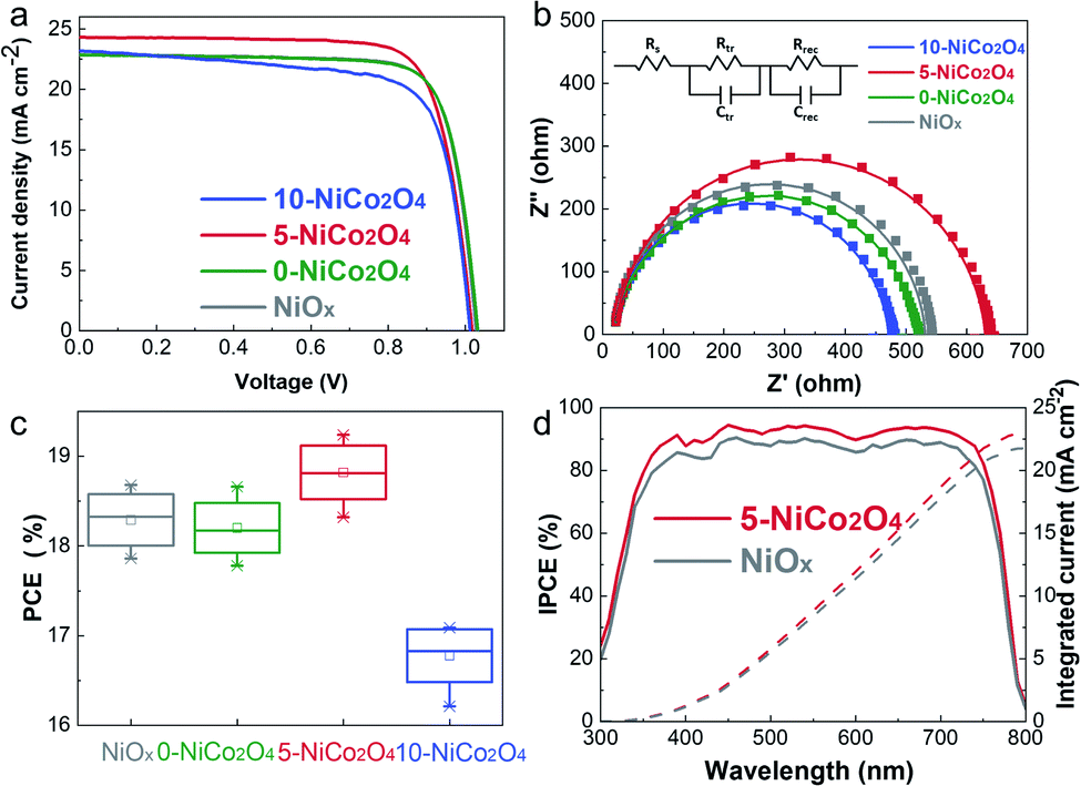 | ||
| Fig. 4 (a) J–V characteristics of best NiOx and NiCo2O4-based PSCs measured under illumination (1 sun). (b) Nyquist plots of PSCs based on NiOx and NiCo2O4 HTLs for electrochemical impedance spectroscopy (EIS) experiments. Solid lines show fitting curves. (c) Statistics of ten pieces of each PSCs based on NiOx and NiCo2O4 HTLs. (d) Incident-photon-to-current efficiencies (IPCEs) of PSCs based on NiOx and 5-NiCo2O4 HTLs under monochromatic light with varying wavelengths. Dashed lines represent corresponding integrating currents over AM 1.5 G solar irradiance spectra. | ||
| HTL | Voc (V) | Jsc (mA cm−2) | FF (%) | PCE (%) |
|---|---|---|---|---|
| NiOx | 1.03 | 22.86 | 79.61 | 18.69 |
| 0-NiCo2O4 | 1.03 | 22.84 | 79.31 | 18.66 |
| 5-NiCo2O4 | 1.02 | 24.31 | 77.89 | 19.24 |
| 10-NiCo2O4 | 1.01 | 23.14 | 73.09 | 17.09 |
EIS measurements were performed to give a closer inspection of the charge transport process and recombination process at the interfaces.14 As shown in Fig. 4b, only one semicircle was observed for each sample, which corresponds to the recombination resistance (Rrec). The largest semicircle belonged to the 5-NiCo2O4 HTL-based device, which revealed that the carrier recombination at the interfaces between the HTL and perovskite layer was retarded. The semicircle of the NiOx device was slightly larger than that of the 0-NiCo2O4-based device, corresponding to the photovoltaic performances of the two devices (Fig. 4a and Table 1). The lowest Rrec was obtained for the 10-NiCo2O4 based device, which correlated well with the observed decreases in Voc and FF. As discussed above, the 5-NiCo2O4 HTL-based PSC had the lowest interfacial recombination loss, which was beneficial for faster charge transfer and collection across the device, thus resulting in a higher PEC. Besides, we measured the dark J–V curves of PSCs incorporated with NiOx and different NiCo2O4 HTLs, as depicted in Fig. S7.† The dark current density decreases in the order of 10-NiCo2O4> NiOx> 0-NiCo2O4 > 5-NiCo2O4, indicating that 5-NiCo2O4-based device possesses better diode behavior with lower leakage current density.
As photocurrent hysteresis was a major issue in the accurate characterization of device efficiency, the typical J–V curves were measured for PSCs based on the NiOx and 5-NiCo2O4 HTLs, with both reverse and forward scan directions (Fig. S8a†). The 5-NiCo2O4 HTL-based PSCs exhibited slight hysteresis in the J–V curves, and the reverse and forward scanning directions yielded PCEs of 19.73 and 19.24%, respectively (a difference of 0.49%, as listed in Table S4†). Meanwhile, the steady-state power output at the maximum power point for the optimized devices was recorded in Fig. S8b,† where the PCE of the 5-NiCo2O4 HTL-based PSC rose directly to a steady-state, yielding a maximum PCE value of 19.37% at 0.87 V. Low hysteresis and the quick photoelectric response could be attributed to the efficient charge separation and transport promoted by 5-NiCo2O4, which significantly suppressed interfacial charge recombination between the HTL and perovskite.16
The incident-photon-to-current efficiencies (IPCEs) of PSCs based on NiOx and 5-NiCo2O4 HTLs were measured (Fig. 4d). As the wavelength was gradually increased from 300 to 800 nm, the IPCE of the PSC based on the 5-NiCo2O4 HTL remained higher than that of the NiOx HTL-based PSC. Moreover, photocurrents of 22.98 mA cm−2 and 21.78 mA cm−2 were obtained by integrating the IPCE curves for PSCs based on 5-NiCo2O4 and NiOx HTLs over the AM 1.5 G solar irradiation spectrum. These values are consistent with the experimentally measured Jsc values.
The long-term stabilities of unencapsulated PSCs based on the 5-NiCo2O4 and NiOx HTLs were investigated in an ambient atmosphere at room temperature with humidity of 30–40% (Fig. 5). As the aging time was extended to approximately 360 h, the PCEs of the device fabricated on the 5-NiCo2O4 HTL remained at 90.7% of the initial efficiency. As a comparison, the PCE of the device based on NiOx HTL retained less than 90% of its initial efficiency after only 288 h aging time under the same condition.
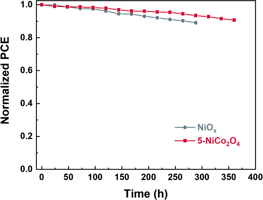 | ||
| Fig. 5 Long-term stability of the devices based on NiOx and 5-NiCo2O4 HTLs stored at ambient conditions with humidity of 30–40%. | ||
Conclusions
For the first time, NiCo2O4 films obtained by ECD method were employed as HTLs to obtain efficient and stable PSCs. Notably, when a suitable amount of KCl additive was added to the deposition solution, a smooth and compact NiCo2O4 layer could be obtained, which was beneficial for the contact of the perovskite layer covered on the NiCo2O4 HTL. Meanwhile, the p-type semiconductor property and electrical conductivity could both be enhanced, leading to efficient charge separation and transport between perovskite and the NiCo2O4 HTL. Thus, a PCE of 19.24% was obtained for the NiCo2O4 HTL-based champion device, with negligible hysteresis, excellent reproducibility, and long-term stability. In addition, this PCE was better than that of a NiOx HTL-based PSC (18.68%). This study shows the huge potential of ECD-prepared NiCo2O4 HTLs for PSCs, and the findings presented here could provide a novel perspective on the preparation of advanced HTLs for further enhancement of PSCs performance and large-scale application.Conflicts of interest
There are no conflicts of interest to declare.Acknowledgements
This work was financially supported by the National Natural Science Foundation of China (NSFC; Grant No. 22172011), and the Key Laboratory of Bio-based Chemicals of Liaoning Province of China. L. Wang thanks Zhejiang Province Selected Funding for Postdoctoral Research Projects (ZJ2021001) for financial support.Notes and references
- X. Zheng, Y. Hou, C. Bao, J. Yin, F. Yuan, Z. Huang, K. Song, J. Liu, J. Troughton, N. Gasparini, C. Zhou, Y. Lin, D.-J. Xue, B. Chen, A. K. Johnston, N. Wei, M. N. Hedhili, M. Wei, A. Y. Alsalloum, P. Maity, B. Turedi, C. Yang, D. Baran, T. D. Anthopoulos, Y. Han, Z.-H. Lu, O. F. Mohammed, F. Gao, E. H. Sargent and O. M. Bakr, Nat. Energy, 2020, 5, 131–140 CrossRef CAS.
- J. Burschka, A. Dualeh, F. Kessler, E. Baranoff, N.-L. Cevey-Ha, C. Yi, M. K. Nazeeruddin and M. Grätzel, J. Am. Chem. Soc., 2011, 133, 18042–18045 CrossRef CAS PubMed.
- D. Stranks Samuel, E. Eperon Giles, G. Grancini, C. Menelaou, J. P. Alcocer Marcelo, T. Leijtens, M. Herz Laura, A. Petrozza and J. Snaith Henry, Science, 2013, 342, 341–344 CrossRef CAS PubMed.
- Best Research Cell Efficiencies, https://www.nrel.gov/pv/assets/pdfs/best-research-cell-efficiencies-rev211117.pdf.
- V. Gonzalez-Pedro, E. J. Juarez-Perez, W.-S. Arsyad, E. M. Barea, F. Fabregat-Santiago, I. Mora-Sero and J. Bisquert, Nano Lett., 2014, 14, 888–893 CrossRef CAS PubMed.
- T. Wu, Z. Qin, Y. Wang, Y. Wu, W. Chen, S. Zhang, M. Cai, S. Dai, J. Zhang, J. Liu, Z. Zhou, X. Liu, H. Segawa, H. Tan, Q. Tang, J. Fang, Y. Li, L. Ding, Z. Ning, Y. Qi, Y. Zhang and L. Han, Nano-Micro Lett., 2021, 13, 152 CrossRef CAS PubMed.
- J. Yan, T. J. Savenije, L. Mazzarella and O. Isabella, Sustainable Energy Fuels, 2022, 6, 243–266 RSC.
- J. H. Noh, N. J. Jeon, Y. C. Choi, M. K. Nazeeruddin, M. Grätzel and S. I. Seok, J. Mater. Chem. A, 2013, 1, 11842–11847 RSC.
- P. Mahajan, B. Padha, S. Verma, V. Gupta, R. Datt, W. C. Tsoi, S. Satapathi and S. Arya, J. Energy Chem., 2022, 68, 330–386 CrossRef.
- J. R. Manders, S.-W. Tsang, M. J. Hartel, T.-H. Lai, S. Chen, C. M. Amb, J. R. Reynolds and F. So, Adv. Funct. Mater., 2013, 23, 2993–3001 CrossRef CAS.
- H. Zhang, H. Wang, H. Zhu, C.-C. Chueh, W. Chen, S. Yang and A. K. Y. Jen, Adv. Energy Mater., 2018, 8, 1702762 CrossRef.
- W. Chen, Y. Wu, Y. Yue, J. Liu, W. Zhang, X. Yang, H. Chen, E. Bi, I. Ashraful, M. Grätzel and L. Han, Science, 2015, 350, 944–948 CrossRef CAS PubMed.
- W. Chen, F.-Z. Liu, X.-Y. Feng, A. B. Djurišić, W. K. Chan and Z.-B. He, Adv. Energy Mater., 2017, 7, 1700722 CrossRef.
- T. Wang, D. Ding, H. Zheng, X. Wang, J. Wang, H. Liu and W. Shen, Sol. RRL, 2019, 3, 1900045 CrossRef.
- F. Igbari, M. Li, Y. Hu, Z.-K. Wang and L.-S. Liao, J. Mater. Chem. A, 2016, 4, 1326–1335 RSC.
- H. Zhang, H. Wang, W. Chen and A. K. Y. Jen, Adv. Mater., 2017, 29, 1604984 CrossRef PubMed.
- P.-L. Qin, Q. He, C. Chen, X.-L. Zheng, G. Yang, H. Tao, L.-B. Xiong, L. Xiong, G. Li and G.-J. Fang, Sol. RRL, 2017, 1, 1700058 CrossRef.
- Z. Wu, Y. Zhu and X. Ji, J. Mater. Chem. A, 2014, 2, 14759–14772 RSC.
- Y. Li, X. Wu, S. Wang, W. Wang, Y. Xiang, C. Dai, Z. Liu, Z. He and X. Wu, RSC Adv., 2017, 7, 36909–36916 RSC.
- C. Zhu, S. Fu, D. Du and Y. Lin, Chem. - Eur. J., 2016, 22, 4000–4007 CrossRef CAS PubMed.
- R. R. Owings, G. J. Exarhos, C. F. Windisch, P. H. Holloway and J. G. Wen, Thin Solid Films, 2005, 483, 175–184 CrossRef CAS.
- F. Yang, X. Tian, Y. Gu, K. Zhang and L. Liu, RSC Adv., 2019, 9, 24880–24887 RSC.
- J. H. Lee, Y. W. Noh, I. S. Jin, S. H. Park and J. W. Jung, J. Mater. Chem. C, 2019, 7, 7288–7298 RSC.
- D. Ouyang, J. Xiao, F. Ye, Z. Huang, H. Zhang, L. Zhu, J. Cheng and W. C. H. Choy, Adv. Energy Mater., 2018, 8, 1702722 CrossRef.
- I. T. Papadas, A. Ioakeimidis, G. S. Armatas and S. A. Choulis, Adv. Sci., 2018, 5, 1701029 CrossRef PubMed.
- A. Bashir, S. Shukla, R. Bashir, R. Patidar, A. Bruno, D. Gupta, M. S. Satti and Z. Akhter, Sol. Energy, 2020, 196, 367–378 CrossRef CAS.
- F. Li, Y. Li, Q. Zhuo, D. Zhou, Y. Zhao, Z. Zhao, X. Wu, Y. Shan and L. Sun, ACS Appl. Mater. Interfaces, 2020, 12, 11479–11488 CrossRef CAS PubMed.
- Z. Zhao, S. Zhan, L. Feng, C. Liu, M. S. G. Ahlquist, X. Wu, K. Fan, F. Li and L. Sun, ACS Appl. Mater. Interfaces, 2021, 13, 40602–40611 CrossRef PubMed.
- T. Wang, D. Ding, X. Wang, R. Zeng, H. Liu and W. Shen, ACS Omega, 2018, 3, 18434–18443 CrossRef CAS PubMed.
- I. J. Park, G. Kang, M. A. Park, J. S. Kim, S. W. Seo, D. H. Kim, K. Zhu, T. Park and J. Y. Kim, ChemSusChem, 2017, 10, 2660–2667 CrossRef CAS PubMed.
- X. Miao, S. Wang, W. Sun, Y. Zhu, C. Du, R. Ma and C. Wang, Scr. Mater., 2019, 165, 134–139 CrossRef CAS.
- R. Tena-Zaera, J. Elias, G. Wang and C. Lévy-Clément, J. Phys. Chem. C, 2007, 111, 16706–16711 CrossRef CAS.
- R. Tena-Zaera, J. Elias, C. Lévy-Clément, C. Bekeny, T. Voss, I. Mora-Seró and J. Bisquert, J. Phys. Chem. C, 2008, 112, 16318–16323 CrossRef CAS.
- Y. Mastai, D. Gal and G. Hodes, J. Electrochem. Soc., 2000, 147, 1435 CrossRef CAS.
- X. Zhang, H. Xiong, J. Qi, C. Hou, Y. Li, Q. Zhang and H. Wang, ACS Appl. Energy Mater., 2018, 1, 6477–6486 CrossRef.
- I. Sullivan, B. Zoellner and P. A. Maggard, Chem. Mater., 2016, 28, 5999–6016 CrossRef CAS.
- A. Barnabé, Y. Thimont, M. Lalanne, L. Presmanes and P. Tailhades, J. Mater. Chem. C, 2015, 3, 6012–6024 RSC.
- Y. Zhang, B. Wang, F. Liu, J. Cheng, X.-w. Zhang and L. Zhang, Nano Energy, 2016, 27, 627–637 CrossRef CAS.
- J. H. Kim, P.-W. Liang, S. T. Williams, N. Cho, C.-C. Chueh, M. S. Glaz, D. S. Ginger and A. K. Y. Jen, Adv. Mater., 2015, 27, 695–701 CrossRef CAS PubMed.
- P. Zhu, S. Gu, X. Luo, Y. Gao, S. Li, J. Zhu and H. Tan, Adv. Energy Mater., 2020, 10, 1903083 CrossRef CAS.
- Y. Chen, Z. Yang, S. Wang, X. Zheng, Y. Wu, N. Yuan, W.-H. Zhang and S. Liu, Adv. Mater., 2018, 30, 1805660 CrossRef PubMed.
Footnote |
| † Electronic supplementary information (ESI) available. See https://doi.org/10.1039/d2ra01816k |
| This journal is © The Royal Society of Chemistry 2022 |