 Open Access Article
Strain engineering of lateral heterostructures based on group-V enes (As, Sb, Bi) for infrared optoelectronic applications calculated by first principles†
Mengying Liu‡
 a,
Weijie Li‡a,
Dan Cheng‡ac,
Xuan Fang*ad,
Hongbin Zhao*b,
Dengkui Wang
 *a,
Jinhua Lia,
Yingjiao Zhaia,
Jie Fana,
Haizhu Wanga,
Xiaohua Wanga,
Dan Fanga and
Xiaohui Maa
aState Key Laboratory of High Power Semiconductor Lasers, School of Physics, Changchun University of Science and Technology, 7089 Wei-Xing Road, Changchun 130022, P. R. China. E-mail: fangx@cust.edu.cn; wangdk@cust.edu.cn
bState Key Laboratory of Advanced Materials for Smart Sensing, General Research Institute for Nonferrous Metals, Beijing, 100088, P. R. China. E-mail: zhaohongbin@ginm.com
cChangchun Guanghua University, 3555 Wu-Han Road, Changchun, 130022, P. R. China
dSchool of Science and Engineering, The Chinese University of Hong Kong, Shenzhen, Guangdong 518172, P. R. China
First published on 13th May 2022
Abstract
In this work, the electronic structure, and optical properties of As/Sb and Sb/Bi lateral heterostructures (LHS) along armchair and zigzag interfaces affected by strain were investigated by density functional theory. The LHSs presented strain-dependent band transformation characteristics and sensitivity features. And a reduction and transition of the bandgap was observed when the As/Sb and Sb/Bi LHS existed under compressive strain. The density of states and the conduction band minimum-valence band maximum characteristics exhibited corresponding changes under the strain. Then a spatial charge-separation phenomenon and strong optical absorption properties in the mid-infrared range can also be observed from calculated results. Theoretical research into As/Sb and Sb/Bi LHSs has laid a solid foundation for As/Sb and Sb/Bi LHS device manufacture.
1. Introduction
The electronic and optical properties of semiconductors are critical features that determine their performance in optoelectronic applications. Strain engineering has been explored and implemented as an efficient approach to improve the performance of photonic and electronic devices.1–4 The electronic, optical, mechanical, magnetic, superconducting, and thermal properties are controlled effectively through strain. For instance, band and electronic structures can be modulated under a unique strain, by an increase or decrease or induction of a direct-to-indirect (or the reverse) transition.5,6 Many strain sources exist, including lattice mismatch between the heterojunction and epitaxy interfaces or deposition processes7–9 and thermal mismatch from the difference in thermal expansion coefficient.9–11 External strain, such as material bending or compression, can also induce strain12–14 In addition, a reduction in dimensions also results in an increased sensitivity of the physicochemical characteristics of materials to strain.As a novel semiconductor type, two-dimensional (2D) materials have superior electronic properties, an optical transparency, a specific surface area, and controllability.15–20 Moreover, 2D materials have a lower bulk defect density and stronger covalent bonding of atoms in the in-plane direction,20–23 compared with bulk materials. Under compressive (or tensile) strain, the lattice structure can be tuned easily and without fracture.24,25 This strong deformation capacity indicates great potential in strain engineering. For example, the phonon structure of 2D materials changes because of lattice structure distortion by uniaxial or biaxial strain, and tensile strain leads to a softening of the phonon mode, and the opposite behavior for compressive strain.25–28 Strain can change the electronic structure of single materials and, thus, increase or decrease carrier mobility. The optical properties of MoS2 are determined from the band gap, which can be adjusted by strain, and the optical properties are reflected by changes in the PL spectrum intensity and the shift in peak position.29,30 Strain is a promising approach to induce and modulate the magnetic properties of monolayer MoS2 through the competitive behavior of through-bond and through-space interactions.31,32 The phase transition of MoTe2 from 2H to 1T involves overall movement of atomic positions, which can be achieved by applying strain.33,34 In the so-called strain state, 2D materials can exhibit extraordinary optical, thermal, electronic, and other properties because of changes in the distance between atoms.14,35–37 Therefore, an investigation of the effect of strain on optoelectronic properties, especially for 2D materials, is important, either from theoretical or experimental aspects.38
Among the numerous monolayer 2D materials, a lateral monolayer heterostructure has been predicted and realized in recent years.38–42 A lateral heterostructure (LHS) can have different atom configuration at the interface, which induces neoteric properties. In this work, we constructed Group-V enes (As, Sb, Bi) monolayer LHSs of As/Sb and Sb/Bi. Two interface atoms that were arranged in the armchair (AC) and zigzag (ZZ) direction were considered. We used a large range of tensile and compressive strains and investigated the characteristics of the energy band and electronic structures under a strain effect for the two LHSs using a first-principles method.
2. Computational details
Density functional theory calculations were carried out by using the Vienna Ab initio Simulation Package (VASP).43 The electronic interaction was described by the projector-enhanced wave (PAW) potential.44 In the generalized gradient approximation (GGA), the Perdew–Burke–Ernzerhof (PBE) functional45 was selected to deal with the exchange-related interaction of electrons. The long-range van der Waals interaction between the atomic layers was handled by the semi-empirical dispersion correction D3 scheme that was proposed by Grimme.46 The Brillouin zone used a k-point grid sampling with uniform intervals of 2π × 0.04 Å−1. The cutoff energy that was selected for the plane wave foundation was 600 eV. To confirm its identity as an energy minimum, vibrational analysis was performed at each stationary point with no imaginary vibrational frequency. The convergence criteria for energy (converged to 1.0 × 10⁻⁵ eV per atom) and force (converged to 0.01 eV Å−1) were set for the geometry optimization. To avoid the interaction between adjacent layers, a vacuum spacing of 15 Å was added along the direction perpendicular to the 2D sheet. The Perdew–Burke–Ernzerhof functional was used to calculate the electronic energy band structure, density of state (DOS), light absorption spectrum, valence band maximum (VBM), and conduction band minimum (CBM) of each 2D LHS.3. Results and discussion
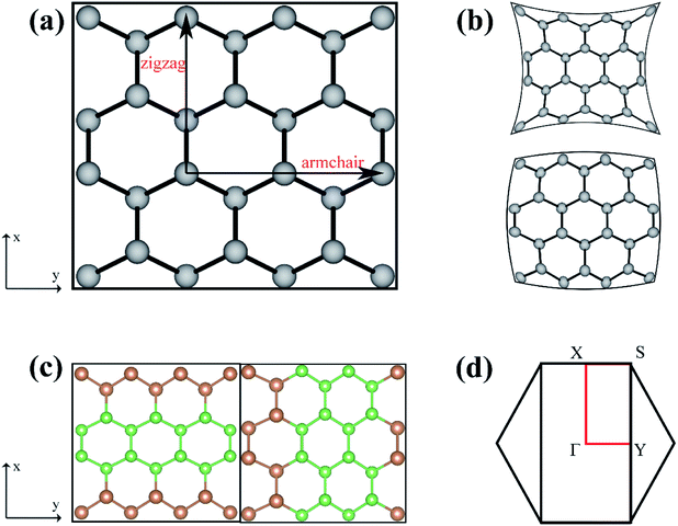
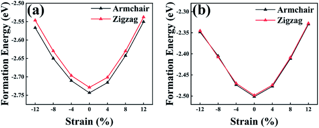
The As, Sb, and Bi monolayer had a puckered honeycomb structure like black phosphorus. Fig. 1(a) shows the top view of the As, Sb or Bi monolayer structure model, in which the AC and ZZ edges of the single layer structure are visible clearly. Compressive or tensile strain application to a single-layer structure results in a slight deformation of the structure. And the related deformation features of the single-layer structure are also presented as shown in Fig. 1(b). Later, we designed and constructed the As2/Sb2 and Sb2/Bi2 LHSs along the ZZ and AC interface, where “2” represents the number of atomic columns on the two sides of the interface.47 The top view of the LHS structure constructed along the ZZ and AC interface is shown in Fig. 1(c). To construct an LHS with a seamless interface, the Brillouin zone was transformed from a hexagon to a rectangle, as shown in Fig. 1(d). The Γ point represents the position of the high symmetry point in the Brillouin zone.The formation energy (Ef) can be used as an evaluation index to ascertain the structural and energetic stability of the constructed LHSs. The Ef is calculated from:
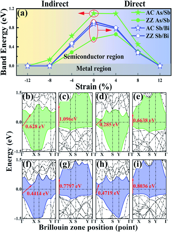
To study the electronic properties of the LHS, we calculated the energy bands of the As/Sb and Sb/Bi LHS. Fig. 3(a) shows the trend of band gap variation with strain, and the band structures of the As/Sb and Sb/Bi LHSs that were constructed along the AC and ZZ at −4% and +4% strain are shown in Fig. 3(b–i) (the band structures at −12%, −8%, 0%, 8%, and 12% strains are shown in Fig. S1 ESI†). The main results can be divided into three parts: (I) the As/Sb LHS had a bandgap transition from indirect to direct through the stitching of different interfaces, as shown in Fig. 3(a). Under the condition of no strain, the As/Sb LHS structure that was constructed along the AC interface had an indirect bandgap of 1.1 eV, where the VBM was located at Γ point and CBM was between Γ point and X point, as shown in Fig. S1.† The As/Sb LHS structure that was constructed along the ZZ interface had a direct bandgap of 0.57 eV, and the VBM and CBM was located at Γ point, respectively. (II) The band structure changed with the change in strain, as shown in Fig. 3(a). For a tensile strain, the AC As/Sb LHS had an indirect-to-direct bandgap transition. The ZZ As/Sb LHS had a direct-to-indirect bandgap transition in the case of a compressive strain. A similar transformation occurred for the Sb/Bi LHS. The compressive strain caused a direct-to-indirect bandgap transition of the Sb/Bi LHS. Regardless of whether a tensile or compressive strain was applied, VBM was located at Γ point, whereas CBM shifted from point Γ point to between T point and X point under a compressive strain. (III) The strain led to shifts toward a Fermi energy of the conduction and valence bands, and a reduction in the band gap of the As/Sb and Sb/Bi LHSs. When a large strain was applied, the As/Sb and Sb/Bi LHSs had a zero band gap state, and at this time, the LHS assumed a metallic state.
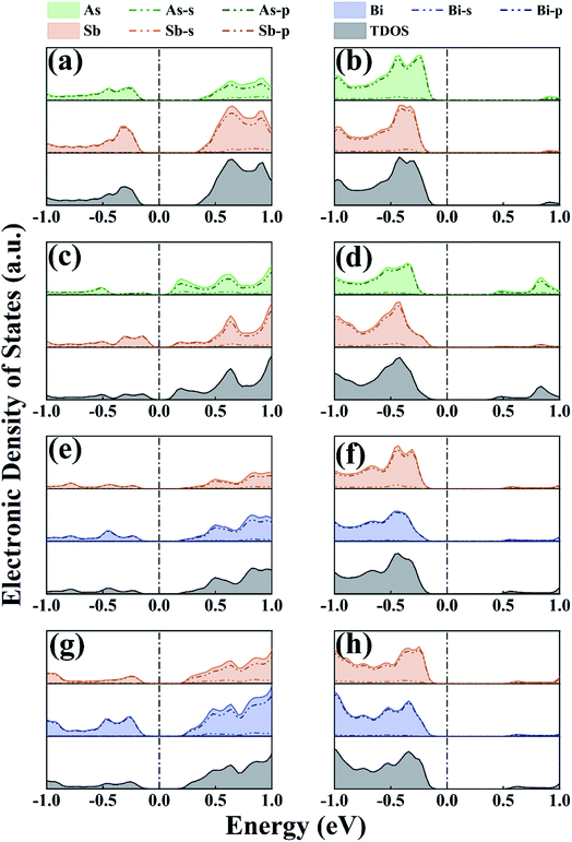
We conducted PDOS and CBM/VBM studies on As/Sb and Sb/Bi LHSs to understand the mechanism of energy band structure change. The PDOS study illustrated the behavior of each atom in the As/Sb and Sb/Bi LHSs under different strains, the position of the conduction and valence bands relative to the Fermi level, and the overall electronic properties in this type of heterostructure. The PDOS calculation results at −4%, 0%, and +4% strains are shown in Fig. 4 (the PDOS for the −12%, −8%, 0%, 8%, and 12% strains are shown in Fig. S2 in the ESI†). For the AC As/Sb LHS, the electrons in the 5p states of Sb were dominant in the conduction and valence band, no matter which type of strain applied (as shown in Fig. 4(a) and (b)), and the occupied states of the ZZ As/Sb LHS conduction bands were mainly contributed to by the 4p states of As, as shown in Fig. 4(c) and (d). The indirect-to-direct band structure transition may be caused by p-orbital hybridization of the As and Sb atoms when the LHS interface changed from the AC to the ZZ. For the Sb/Bi LHS, the electrons in the 6p states of Bi were dominant in the conduction and valence band, no matter which type of strain applied (as shown in Fig. 4(e)–(h)). After tensile strain application, the contribution of the 4p state of As in the conduction and valence bands of the As/Sb LHS increased, and the contribution of the 5p state of Sb in the conduction and valence bands of Sb/Bi LHS increased. When strain was applied to the As/Sb and Sb/Bi LHS, the state moved to the Fermi level, which resulted in a gradual decrease in band gap and an increase in local density of states at the Fermi level. At a strain of −12%, −8%, or 12%, the atomic orbital passed through the Fermi level, and the As/Sb and Sb/Bi LHS band gap was reduced to zero, which shows the characteristics of the metal.
Atoms in the As/Sb and Sb/Bi LHSs showed a strong interaction because of the covalent bond connection; therefore, the electronic state between the interfaces was the focus of research. To illustrate the charge distribution on the LHS, we plotted the VBM and CBM 2D band-decomposed charge densities of the As/Sb and Sb/Bi LHS under different levels of strain, as shown in Fig. 5. For metallic state of LHS (applied with large levels of strain), when compressive strain is applied, the state of As/Sb LHS is distributed around Sb atoms, and the state of Sb/Bi LHS is distributed around Bi atoms; on the contrary, the state of LHS The states are distributed around two kinds of atoms when tensile strain is applied. The VBM states for the As/Sb and Sb/Bi LHSs were distributed at the bonds, whereas the CBM states were distributed around the atoms of LHSs. After tensile strain application, the VBM state of the AC As/Sb LHS changed to being localized around the As monolayers, whereas the CBM state of the AC As/Sb LHS changed to being distributed around the As and Sb atoms. At a +8% strain, the VBM state of the ZZ As/Sb LHS changed to being located around the As monolayers. A similar situation occurred for the Sb/Bi LHS. Under a tensile strain, the VBM state of the Sb/Bi LHS changed to being localized around the Sb monolayers.
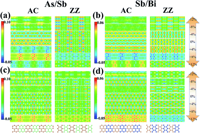 | ||
| Fig. 5 (a) valence band maximum (VBM) of As/Sb lateral heterostructure (LHS), (b) VBM of Sb/Bi LHS, (c) conduction band minimum (CBM) of As/Sb LHS, (d) CBM of Sb/Bi LHS. | ||
Previous research showed that the optical absorption rate can be used to characterize the optical properties of any system that contains 2D sheets. Fig. 6 shows the relationship between the absorption spectra of the As/Sb and Sb/Bi LHSs with wavelength. As shown in Fig. 6(a) and (b), the optical absorption, of As/Sb LHS, in the YY direction was weak compared with that in the XX direction. The opposite happened for the Sb/Bi LHS, where the optical absorption in the YY direction was stronger compared with that in the XX direction, as shown in Fig. 6(c) and (d). Compared with the optical absorption of the LHS at no strain, the absorption spectra of LHS changed in scope and intensity with the change in strain. When a compressive strain was applied to the Sb/Bi and AC As/Sb LHSs, the light absorption intensity increased, and the absorption edge moved to a short-wave direction. However, when a tensile strain was applied to the Sb/Bi and AC As/Sb LHSs, the light absorption intensity decreased, and the absorption edge moved to a long wave direction. These results indicate that As/Sb and Sb/Bi LHSs have potential application in optical elements.
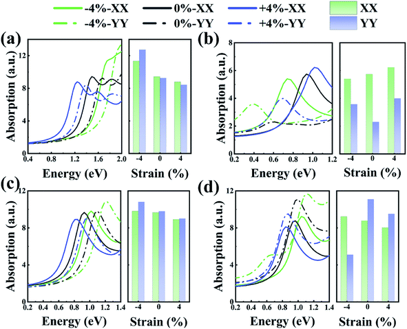 | ||
| Fig. 6 Light absorption at different strains for (a) armchair (AC) As/Sb lateral heterostructure (LHS), (b) zigzag (ZZ) As/Sb LHS, (c) AC Sb/Bi LHS, (d) ZZ Sb/Bi LHS. | ||
4. Conclusion
The structural, formation energy, electronic, and optical properties of As/Sb and Sb/Bi LHSs were investigated through density functional theory. We examined the As/Sb and Sb/Bi LHS formation energy properties of two interface structures at different strain levels. The predicted As/Sb and Sb/Bi LHSs were energetically favorable and are expected to be synthesized under controlled experimental conditions. An evaluation of the external strain for As/Sb and Sb/Bi validates that the bandgap can be engineered by the compressive or tensile strain. DOS, PDOS, and CBM/VBM studies on the As/Sb and Sb/Bi LHSs showed that the reason for the change in energy band structure was the change in electronic state. The calculated optical properties showed that the absorption rate of the spectrum changed in range and intensity with the change in strain. Our theoretical studies show that the constructed As/Sb and Sb/Bi LHSs have potential applications in nanoelectronics and optical devices.Conflicts of interest
The authors declare that they have no known competing financial interests or personal relationships that could have appeared to influence the work reported in this paper.Acknowledgements
This work is supported by the National Natural Science Foundation of China (62074018, 62174015), the Developing Project of Science and Technology of Jilin Province (20200301052RQ, 20210509061RQ), the Natural Science Foundation of Jilin Province (20210101150JC, 20210101473JC, 20200201266JC), the Project of Education Department of Jilin Province (JJKH20210831KJ), the Natural Science Foundation of Guangdong Province (2020A1515010868) and the Shenzhen Fundamental Research Fund (JCYJ20180307151538972).References
- Z. H. Dai, L. Q. Liu and Z. Zhang, Adv. Mater., 2019, 31, 1805417 CrossRef CAS PubMed.
- J. L. Du, H. H. Yu, B. S. Liu, M. Y. Hong, Q. L. Liao, Z. Zhang and Y. Zhang, Small Methods, 2021, 5, 2000919 CrossRef CAS PubMed.
- S. X. Yang, Y. J. Chen and C. B. Jiang, InfoMat, 2021, 3, 397–420 CrossRef.
- B. W. Zhang, D. Fang, X. Fang, H. B. Zhao, D. K. Wang, J. H. Li, X. H. Wang and D. B. Wang, Rare Metals, 2021, 41, 982–991 CrossRef.
- Y. H. Wang, J. B. Pang, Q. L. Cheng, L. Han, Y. F. Li, X. Meng, B. Ibarlucea, H. B. Zhao, F. Yang, H. Y. Liu, H. Liu, W. J. Zhou, X. Wang, M. H. Rummeli, Y. Zhang and G. Cuniberti, Nano-Micro Lett., 2021, 13, 52 CrossRef PubMed.
- Q. Pei, X. C. Wang, J. J. Zou and W. B. Mi, Nanotechnology, 2018, 29, 9 Search PubMed.
- A. Ohtake, T. Mano and Y. Sakuma, Sci. Rep., 2020, 10, 7 CrossRef PubMed.
- E. Koo, Y. Lee, Y. Song, M. Park and S. Y. Ju, ACS Appl. Electron. Mater., 2019, 1, 113–121 CrossRef CAS.
- A. Moridi, H. H. Ruan, L. C. Zhang and M. Liu, Int. J. Solids Struct., 2013, 50, 3562–3569 CrossRef.
- E. T. Ritz and N. A. Benedek, Phys. Rev. Mater., 2020, 4, 7 Search PubMed.
- F. Wang, B. Zhou, H. M. Sun, A. Y. Cui, T. Jiang, L. P. Xu, K. Jiang, L. Y. Shang, Z. G. Hu and J. H. Chu, Phys. Rev. B, 2018, 98, 9 Search PubMed.
- W. Wu, J. Wang, P. Ercius, N. C. Wright, D. M. Leppert-Simenauer, R. A. Burke, M. Dubey, A. M. Dogare and M. T. Pettes, Nano Lett., 2018, 18, 2351–2357 CrossRef CAS PubMed.
- J. Liang, J. Zhang, Z. Li, H. Hong, J. Wang, Z. Zhang, X. Zhou, R. Qiao, J. Xu and P. Gao, Nano Lett., 2017, 17, 7539–7543 CrossRef CAS PubMed.
- S. Yang, C. Wang, H. Sahin, H. Chen, Y. Li, S. S. Li, A. Suslu, F. M. Peeters, Q. Liu and J. Li, Nano Lett., 2015, 15, 1660–1666 CrossRef CAS PubMed.
- K. S. Novoselov, A. K. Geim, S. V. Morozov, D. Jiang, Y. Zhang, S. V. Dubonos, I. V. Grigorieva and A. A. Firsov, Science, 2004, 306, 666–669 CrossRef CAS PubMed.
- B. Radisavljevic, A. Radenovic, J. Brivio, V. Giacometti and A. Kis, Nat. Nanotechnol., 2011, 6, 147–150 CrossRef CAS PubMed.
- L. Li, Y. Yu, G. J. Ye, Q. Ge, X. Ou, H. Wu, D. Feng, X. H. Chen and Y. Zhang, Nat. Nanotechnol., 2014, 9, 372–377 CrossRef CAS PubMed.
- M. Dávila, L. Xian, S. Cahangirov, A. Rubio and G. L. Lay, New J. Phys., 2014, 16, 3579–3587 CrossRef.
- M. Pumera and Z. Sofer, Adv. Mater., 2017, 29, 1605299 CrossRef PubMed.
- C. V. Nguyen, Phys. Rev. B, 2021, 103, 115429 CrossRef CAS.
- G. G. Naumis, S. Barraza-Lopez, M. Oliva-Leyva and H. Terrones, Rep. Prog. Phys., 2017, 80, 1–62 CrossRef PubMed.
- M. A. Bissett, M. Tsuji and H. Ago, Phys. Chem. Chem. Phys., 2014, 16, 11124–11138 RSC.
- H. J. Jiang, L. Zheng, Z. Liu and X. W. Wang, InfoMat, 2020, 2, 1077–1094 CrossRef CAS.
- G. Cocco, E. Cadelano and L. Colombo, Phys. Rev. B: Condens. Matter Mater. Phys., 2010, 81, 2010–2020 CrossRef.
- C. Nguyen, N. V. Hoang, H. V. Phuc, A. Y. Sin and C. V. Nguyen, J. Phy. Chem. Lett., 2021, 12, 5076–5084 CrossRef CAS PubMed.
- Y. Li, Z. Hu, S. Lin, S. K. Lai, J. Wei and P. L. Shu, Adv. Funct. Mater., 2017, 27, 1600986 CrossRef.
- T. M. G. Mohiuddin, A. Lombardo, R. R. Nair, A. Bonetti, G. Savini, R. Jalil, N. Bonini, D. M. Basko, C. Galiotis and N. Marzari, Phys. Rev. B: Condens. Matter Mater. Phys., 2008, 79, 205433 CrossRef.
- D. Yoon, Y. W. Son and H. Cheong, Phys. Rev. Lett., 2011, 106, 155502 CrossRef PubMed.
- K. He, C. Poole, K. F. Mak and J. Shan, Nano Lett., 2013, 13, 2931–2936 CrossRef CAS PubMed.
- H. J. Conley, B. Wang, J. I. Ziegler, R. F. Haglund, S. T. Pantelides and K. I. Bolotin, Nano Lett., 2013, 13, 3626–3630 CrossRef CAS PubMed.
- W. S. Yun and J. D. Lee, J. Phys. Chem. C, 2015, 119, 2822–2827 CrossRef CAS.
- W. Xu, S. M. Yan and W. Qiao, RSC Adv., 2018, 8, 8435–8441 RSC.
- S. Song, D. H. Keum, S. Cho, D. Perello, Y. Kim and Y. H. Lee, Nano Lett., 2015, 16, 188–193 CrossRef PubMed.
- Y. Zhao, Y. Li, M. Liu, K. Xu and F. Ma, J. Phys. Chem. C, 2020, 124, 4299–4307 CrossRef CAS.
- S. B. Desai, G. Seol, J. S. Kang, H. Fang and A. Javey, Nano Lett., 2014, 14, 4592–4597 CrossRef CAS PubMed.
- Y. L. Wang, C. X. Cong, W. H. Yang, J. Z. Shang, N. Peimyoo, Y. Chen, J. Y. Kang, J. P. Wang, W. Huang and T. Yu, Nano Res., 2015, 8, 2562–2572 CrossRef CAS.
- S. Yang, Y. Liu, M. Wu, L. D. Zhao, Z. Lin, H. C. Cheng, Y. Wang, C. Jiang, S. H. Wei and L. Huang, Nano Res., 2018, 011, 554–564 CrossRef CAS.
- C. Q. Nguyen, Y. S. Ang, S.-T. Nguyen, N. V. Hoang, N. M. Hung and C. V. Nguyen, Phys. Rev. B, 2022, 105, 045303 CrossRef CAS.
- Y. Zhao, S. Tan and G. Ouyang, J. Phys. D: Appl. Phys., 2021, 54, 145107 CrossRef CAS.
- T. Huang, J.-C. Lian, K. Yang, Y. Si, H.-Y. Wu, W.-Q. Huang, W. Hu and G.-F. Huang, Phys. E, 2020, 118, 113962 CrossRef CAS.
- J. Yuan, N. Yu, J. Wang, K.-H. Xue and X. Miao, Appl. Surf. Sci., 2018, 436, 919–926 CrossRef CAS.
- Z. Li, J. Zheng, Y. Zhang, C. Zheng, W.-Y. Woon, M.-C. Chuang, H.-C. Tsai, C.-H. Chen, A. Davis, Z.-Q. Xu, J. Lin, H. Zhang and Q. Bao, ACS Appl. Mater. Interfaces, 2017, 9, 34204–34212 CrossRef CAS PubMed.
- G. G. Kresse and J. J. Furthmüller, Phys. Rev. B: Condens. Matter Mater. Phys., 1996, 54, 11169 CrossRef CAS PubMed.
- G. Kresse and D. Joubert, Phys. Rev. B: Condens. Matter Mater. Phys., 1999, 59, 1758–1775 CrossRef CAS.
- J. P. Perdew, K. Burke and M. Ernzerhof, Phys. Rev. Lett., 1996, 77, 3865–3868 CrossRef CAS PubMed.
- S. Grimme, J. Antony, S. Ehrlich and H. Krieg, J. Chem. Phys., 2010, 132, 154104 CrossRef PubMed.
- W. J. Li, X. Fang, D. K. Wang, F. Tian, H. Z. Wang, D. Fang, J. H. Li, X. Y. Chu, H. B. Zhao, D. B. Wang and X. H. Ma, Phys. E, 2021, 134, 114933 CrossRef CAS.
Footnotes |
| † Electronic supplementary information (ESI) available. See https://doi.org/10.1039/d2ra02108k |
| ‡ M. Y. Liu, W. J. Li and D. Cheng contributed equally to this work. |
| This journal is © The Royal Society of Chemistry 2022 |

