DOI:
10.1039/D2RA04181B
(Review Article)
RSC Adv., 2022,
12, 24518-24554
Impact of strain engineering and Sn content on GeSn heterostructured nanomaterials for nanoelectronics and photonic devices
Received
6th July 2022
, Accepted 6th August 2022
First published on 30th August 2022
Abstract
Heterostructures based on the GeSn nanocompound have high impact on integrated photonics devices. The promising feature of GeSn nanostructures is its direct bandgap transition that is a result of Sn incorporation in the Ge networks, forming a strained structure. Herein, we demonstrate a deep survey of the strain-controlling mechanisms in GeSn nanomaterials with different methodologies. Using either layer configurations, Sn incorporation, or by external stressors, the emission of different photonic and nanoelectronic applications is controlled. We find that strain engineering modulates the bandgap of GeSn active media to control the region of emission for light emitting diodes, lasing applications, and spectral response for photodetection applications within the mid-IR region of the spectrum and enhances the performance of MOSFETs. This gives GeSn nanocompounds the chance to contribute greatly to IoT physical devices and compete with unstable perovskite materials since GeSn materials can achieve a stable and more reliable performance.
1. Introduction
To meet the demand of the IoT era and control physical electronic devices through a network, controllable spectral sensitive materials should be developed that can be applied in all the required applications.1 Ge/Si-based photonic and electronic nanomaterials have witnessed a revolution in the last five decades in Si-based optoelectronic integration.2–4 Si and Ge have indirect bandgap that is not favorable in optoelectronic applications.5 The direct bandgap has higher absorption and high emission compared to the indirect one, which is highly needed in photonic transition. Thus, direct transition materials are the promising in photoemission and photodetection applications.6 The incorporation of Sn inside the Ge or Si network allows the direct transition because of the tailored strain to achieve direct bandgap semiconductors.7 Sn has lattice constants larger than that of Ge and Si, which causes a compressive strain in the Ge network.7,8 The value of the strain depends on the Sn content in the Ge network, which increases with the increase in Sn incorporation.9 Many groups have reviewed the direct transition of binary GeSn and ternary SiGeSn as efficient light emitters. J. Menéndez et al. reviewed the extent of directness of the binary GeSn transition. They found that direct transition for radiative emission happens when the Sn content is 8% or more. However, some of the charge carriers directly transit from the valence band to the conduction band, but most carriers transit indirect to the L valley. At room temperature, only 25% of the transitions are direct and below 77 K, 65% of the transitions are direct as the cooling temperature minimizes the energy difference between the direct and indirect valleys. They reported that ternary SiGeSn has different band edges between its elements; hence, it has large bowing parameters that suppress sufficient direct transitions for efficient light emission.10 Wei Du et al. reviewed the challenges met in the incorporation of low temperature grown Sn within high temperature grown Ge. They reviewed how this problem was overcome via the virtual substrate on which dislocations were present due to lattice mismatch between Sn and Ge, causing a reduction of the Sn solubility in Ge. Sn was gradually incorporated in Ge, and then the upper layer relaxed to absorb a higher content of Sn gradually. They reviewed the enhancement of direct photoluminescence via cooling temperature and the electroluminescence for GeSn light emission applications. They also reported the works that investigated cut-off wavelength control in terms of Sn content for GeSn photodetection applications.11 S. Wirths et al. schematically reviewed the band structures of the ternary SiGeSn and the challenges in Sn incorporation within the Ge network, and how it was solved via the homoepitaxial or heteroepitaxial growth of the graded Sn content GeSn layers. They illustrated the mechanism of the GeSn growth via CVD and the history of GeSn preparation by MBE since 1988, passing through preparation trials with CVD till the fabrication of GeSn heterostructure devices for electronic and optoelectronic applications. They also reviewed the impact of Sn on Ge strain and on the shifting of the PL peak toward lower energies. They illustrated GeSn microdisks preparation for lasing emission applications in terms of cooling temperatures.7 Richard Geiger et al. reviewed the effect of Sn incorporation on the indirect L and direct Γ valleys. They reviewed microstrain engineering via microbridge for biaxial strain, stressor layers, and microfins. They reviewed the challenges that are encountered by radiative transitions in GeSn compounds such as Auger recombination and intervalence band absorption due to the valence splitting to heavy hole and light hole levels caused by heavy doping. They showed the calculations of the non-radiative recombination lifetime for GeSn and enhanced PL emission as a function of optically pumped power density.12 Yuanhao Miao et al. reviewed the GeSn growth by CVD and the effect of the growth temperature on the reduction of the Sn content due to the segregation of Sn at high growth temperatures. They demonstrated the effect of the carrier gas in increasing the rate of Sn incorporation and the suppression of Sn incorporation with increasing concentration of SnCl4 precursor as Cl atoms isolate Sn to incorporate in the Ge network. They reviewed the enhancement of PL as a function of growth temperature and optical pumping power for lasing applications. They reviewed the pump power threshold for the prepared GeSn microcavities and the doping concentration of the fabricated p–n heterostructures based on GeSn via As- or B-based precursors.13 David J. Lockwood et al. reviewed in part 3 and 4 in their book strain engineering mechanisms and GeSn alloying to fabricate heterostructures based on GeSn for light emission applications.14
Many attempts have been reported for the optimization of Sn content for direct transition in GeSn compounds. Other experiments were carried out to achieve tensile strain by an external stressor for bandgap modulation. Sn content can also tune the bandgap value of Ge.15–17 Heterostructures were employed for this target. Multiquantum wells (MQWs) were used for confining the carrier transitions and controlling the bandgap value via the thickness adjustment of MQWs.18 In our previous work, we developed a method for tuning the bandgap of GeSn-based compounds over a wide range from UV to NIR.16 It depends on the incorporation of O atoms during the annealing of GeSn compounds under low vacuum conditions, forming GeOx. GeSn-based heterostructures exhibited lasing performance via patterned microdisks as lasing cavities of GeSn with specific dimensions that have threshold power density.19 Stimulated emission occurs and when the threshold pump power is decreased, emission undergoes spontaneously. Thus, GeSn compounds get higher attention in photonic integrated circuits. In this review, we will show how the strain in GeSn is controlled either by the Sn content or using external strain engineering techniques. We will also demonstrate how the emission of GeSn is controlled by different means for LED and lasing applications, and the featured parameters of GeSn MOSFETs are controlled by the relaxation of strain in GeSn. This will allow the reader to understand the control of GeSn bandgap for photonic and nanoelectronic applications.
1.1. Strain engineering in GeSn heterostructure nanocompounds
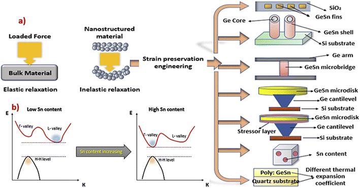
Many attempts have been made to control the stress/strain phenomena in the GeSn heterostructure, as shown in Fig. 1, to modulate their energy gap and create direct transition as well as the bandgap tuning. Strain is a distortion in the bond length and orientation, resulting in lattice constants' change.20 The nanomaterials can achieve high value of strain before yielding compared to the bulk materials that exhibit strain failure at very low value (0.1%).21 Herring et al. reported that 1.8 μm diameter tin wires have 2–3% elastic strain; however, the bulk form has only 0.01% elastic strain.22 Thus, nanostructures can help in achieving higher efficient strain than the bulk form (see the left side in Fig. 1a), which can serve in the fabrication of direct transition GeSn-based nanostructures.
 |
| | Fig. 1 Strain engineering in GeSn compounds; (a) loaded forces effects in bulk and nanostructured materials, (b) effect of Sn incorporation as substitutional content in GeSn transforms the transition from indirect to direct transition via band mixing. | |
Here, different configurations that influence the control of the strain and Ge bandgap are shown in Fig. 1a (right side). To achieve the strain in the structure, the stressor should influence on the molecular configurations of Ge itself. However, Sn incorporation changes the orientations and bond strength because of atomic radii changes in Sn and Ge, forming a compressively strained GeSn network that must be relaxed. Also, the incorporation of Sn modulates the valley of the conduction band of Ge, thus, the band transitions of the charge carriers undergo direct transition, as shown in Fig. 1b. Other means of strain control are the outer stressors that are not incorporated within the structures such as core/shell Ge/GeSn growth, stressor covering layers, arms holding GeSn bridges, heat treatment on mismatching substrates, and suspension of GeSn and GeSn configured growth shown in Fig. 1a (right side).
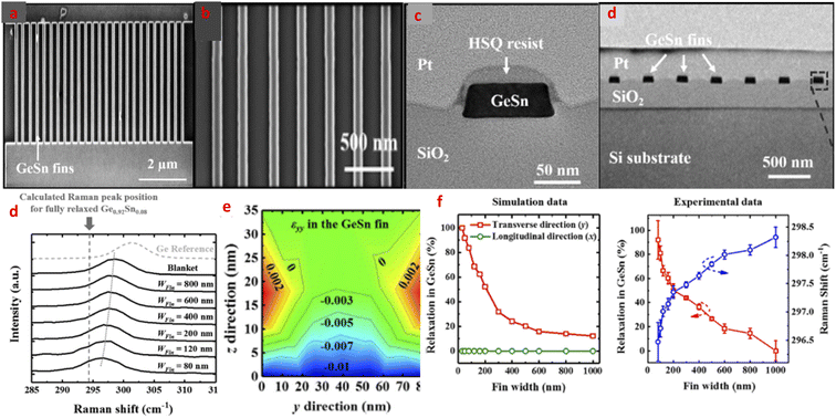
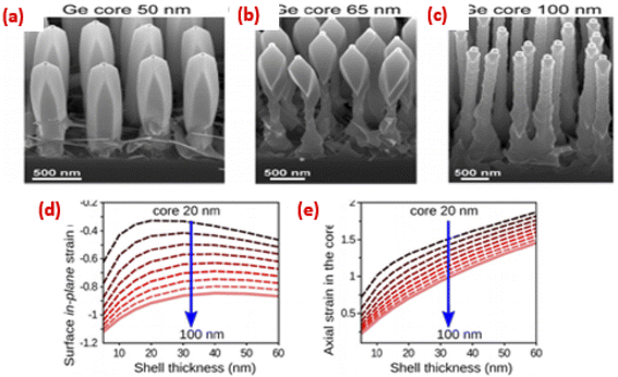
Many attempts have been explored to control the stress/strain phenomena in GeSn heterostructure compounds, as shown in Fig. 1, to modulate their energy gap and create the direct transition as well as bandgap tuning. For example, the relaxation of patterned fin structures Ge1−xSnx Bi-axial strain was studied using micro-Raman spectroscopy by Yuye Kang et al.23 The structural strain was controlled by different fin widths (Wfin), as shown in Fig. 2a–d. 8% Sn content causes −1% compressive strain in Ge1−xSnx, which was obtained when the width of the fin is in the range between 800 nm and 80 nm using Vegards' law.24 Also, Raman investigations showed the shift of the GeSn peak to lower wavenumber due to the decrease in the fin width (Fig. 3d). The transverse direction of strain relaxation increases with a decrease in the fin's width, as shown in Fig. 2e. Fig. 2f shows how the simulation data indicates that strain only transversely relaxes and reaches complete relaxation when the fin width is lowered down to less than 30 nm. Uniaxial compressive strain of Ge1−xSnx can be achieved from biaxial compressive strain of the Ge1−xSnx layer via Ge1−xSnx nanoscale fins patterning. This patterned structure can achieve higher hole mobility in Ge1−xSnx in nanoelectronic devices compared with the biaxially strained Ge1−xSnx channel p-FETs.25,26 Bulk germanium cannot achieve perfect strain for the direct transition at room temperature; thus, nanowire geometry is required for dominant strain.27–29 S. Assali et al. grew arrays of Ge/GeSn core/shell nanowires catalyzed by Au in a CVD reactor; they also illustrated strain control via Ge/GeSn core/shell thicknesses and investigated the optimum conditions of the high strain on large cores thickness and high Sn contents (Fig. 3a–c). The detected defects were obtained at 100 nm Ge cores and only 60 nm GeSn shell growth conditions.30 Thus, the presence of large strain energy was achieved at a smaller shell thickness with similar Sn content and larger Ge cores diameter,31 as shown in Fig. 3(d and e).
 |
| | Fig. 2 GeSn fin structure and strain dependence on Wfins. “Reproduced from ref. 23 https://aip.scitation.org/doi/full/10.1063/1.5012559 CC BY 4.0”. | |
 |
| | Fig. 3 Au-catalyzed arrays of Ge/GeSn core/shell NWs and strain dependence on core diameter. “Reproduced from ref. 30 with permission from [American Institute of Physics publisher], copyright [2019]”. | |
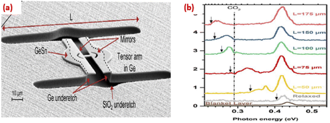
Another engineered design that controls the strain was performed by Jérémie Chrétien et al.32 They illustrated the fabrication of tensile-strained Ge bridges in terms of Ge arms' length on both sides of the Ge microbridge. Arms relaxation and contraction induced by SiO2 insulating layer under etching causes longitudinal stretch of the bridge opposition to Ge epilayers, as shown in Fig. 4a, because of the different compressive radical strain of GeSn alloys as Sn exists in the Ge network.33,34 Fig. 4b shows the shift in the PL emission peak of direct transition GeSn with the increase in the arm length L.
 |
| | Fig. 4 Tensile-strained Ge bridges via side Ge arms and strain dependence on the arm length. “Reproduced from ref. 32 with permission from [American Chemical Society publisher], copyright [2019]”. | |
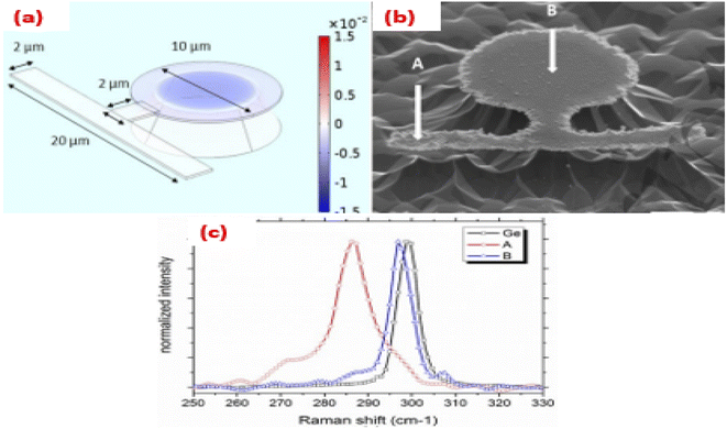
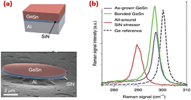
Yi Han et al. designed another configuration to eliminate the compressive strain between GeSn and Ge buffer, and to maintain tensile strain in GeSn for direct transition. They fabricated microdisks of GeSn suspended on Ge buffer above the Si substrate.35 The GeSn microstructure is composed of a suspended cantilever released from the underlying Ge substrate employed to relax the compressively strained suspended microdisk. Fig. 5a–c shows shifting in the Raman peak of the relaxed GeSn microdisk labeled B compared to the compressed Ge buffer labeled A. Another trail by Anas Elbaz et al., in which they used stressor SiNx layer with 350 nm thick that has an intrinsic stress of the value −1.9 GPa, caused tensile strain in the grown of GeSn microdisks.36 This stressor layer causes a shift in the Raman peak by 9 cm−1 when compared with the as-grown GeSn, as shown in Fig. 6a and b.
 |
| | Fig. 5 Microdisks of GeSn suspended on Ge buffer above Si substrate structure and Raman shifting due to the strained GeSn MD. “Reproduced from ref. 35 with permission from [IOPscience publisher], copyright [2018]”. | |
 |
| | Fig. 6 The effect of the SiN stressor layer in the strained GeSn MD. “Reproduced from ref. 36 with permission from [nature publishing group], copyright [2020]”. | |
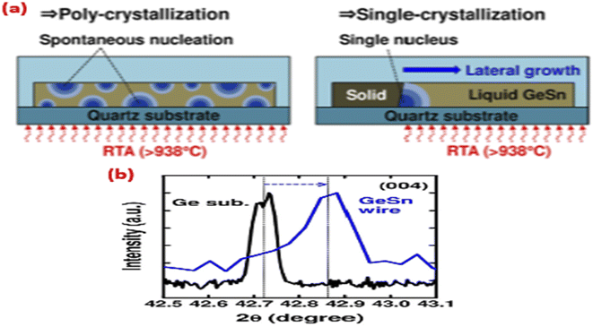
When two layers of two different thermal expansion coefficients are heated together, they certainly influence each other via strain.37,38 Hiroshi Oka et al. utilized this phenomenon to fabricate a single crystalline GeSn compound. This process is known as liquid phase crystallization that requires no crystal-seed. A highly tensile-strained GeSn layer was obtained as a result of thermal expansion coefficient mismatch between GeSn and quartz, as illustrated in Fig. 7a.39 By annealing these two different GeSn compounds on the quartz substrate, a shift in the peak position was caused in the XRD pattern of the prepared GeSn compared to the Ge reference substrate, as shown in Fig. 7b.
 |
| | Fig. 7 A highly tensile-strained GeSn layer was obtained because of thermal expansion coefficient mismatch between GeSn and quartz. “Reproduced from ref. 39 with permission from [American Institute of Physics publisher], copyright [2017]”. | |
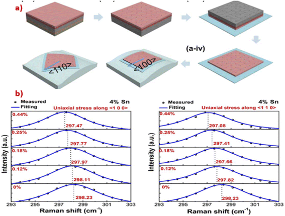
Some experiments employed nanomembrane bending on flexible substrates to release the compressive strain and make tensile-strained GeSn-based structures. Y. Tai et al. designed a mechanically flexible nanomembrane of very low dimension GeSn nanostructure. 370 nm GeSn layer deposited via two-step deposition annealing relaxed the Ge buffer on the buried oxide above the Si substrate. 3 μm NMs array of GeSn were patterned using lithography and chemical etching to make a hole-like shape, and then GeSn were fully relaxed. Raman spectroscopy revealed that the GeSn peak shifted to lower wavenumbers than the as-grown GeSn and bulk Ge to obtain fully-relaxed transfer-printed GeSn.40 The same group studied the same-structured strained GeSn nanomembranes deposited on printed flexible polyethylene terephthalate (PET) substrates via Raman spectroscopy (Fig. 8a). They applied mechanical strain of values 0.12%, 0.18%, 0.25%, and 0.44% on the flexible NM. They reported that the Raman peak of the GeSn mode shifted toward low wavenumbers with increasing external mechanical bending. They reached a uniaxial tensile strength of the bent GeSn NM strain up to 0.44% along the (100) and (110) directions, as seen in Fig. 8b.41 Q. Chen et al. fabricated the GeSn NM photodetector. They deposited doped and undoped GeSn layers on two-step grown Ge buffer on the Si/a-Si/SiO2 stack substrate. Standard lithography and chemical etching were used to pattern similar hole of NMs of the relaxed GeSn; then, reactive ion etching was employed to interdigitate the electrodes. Raman spectroscopy confirms the strain relaxation of GeSn NMs through peak shifting. This relaxed GeSn NM affected the characteristics of PD. They obtained a responsivity of 0.51 A W−1 at 2000 nm when it was biased by 2 V. The responsivity peak shifted toward long wavelengths with increasing NM thickness.42 Shu An et al. fabricated a TiN/GeSn NM flexible heterostructure photodetector formed by the Schottky barrier height of 0.49 eV; the cut-off wavelength extended to 2530 nm and had higher responsivity than the GeSn-based PDs. The tensile strain in the flexible GeSn NM raises the responsivity from 148.5 up to 218 mA W−1 at 0.3% tensile strain.43
 |
| | Fig. 8 (a) Strained GeSn nanomembranes deposited on the printed flexible polyethylene terephthalate (PET) substrates, (b) Raman shifting of GeSn NM on PET substrates in terms of external mechanical bending. “Reproduced from ref. 41 with permission from [IOPscience publisher], copyright [2021]”. | |
1.2. Impact of Sn content on strained GeSn
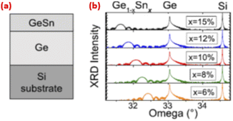
As the diameter of Sn is larger than Ge,44,45 the incorporation of Sn inside the Ge network causes an increase in the compressive strain of the germanium network, causing a dislocation in the structure.46,47 This residual pressure of the caused strain enhances the band mixing between Sn and Ge. Ge is an indirect bandgap element; thus, it has limited use in photonic applications.48 Ge valence band has L–H (low hole) level and H–H (high hole) lower energy level, and it has two valleys composed of the conduction band, L valley that is the indirect higher energy unaligned to the H–H level. The r valley is a direct lower energy than that aligned to the H–H level. Indirect transition in Ge happens between the L valley, L–H, and H–H levels and never undergoes transition directly since ΔEr−L ≠ 0. As the Sn is incorporated in the Ge network, residual pressure causing band mixing between Ge conduction valleys and Sn conduction valleys forms modulated dL valley and r valley with ΔEr−L = 0. Then, the transition in the GeSn compound occurs directly between r-aligned direct valley, L–H, and H–H levels,49–51 as shown in Fig. 9. Some studies have showed that the Sn content has an impact on GeSn strain. A. Gassenq et al. grew GeSn on the Ge buffer above the Si substrate. The growth temperature was varied in the range of 300–350 °C to reach different Sn concentrations (6–15%), as seen in Fig. 10a. GeSn with 15% Sn content sample lattice constant matches with the Ge (VS).52 This GeSn layer is completely strained on the Ge buffer layer. Fig. 10b shows peak position shift toward lower values as the Sn content increases. Omega (ω) plot versus intensity shows a greater shift of the peak position for an Sn concentration of 15%.
 |
| | Fig. 9 Band diagram of Ge and the strained GeSn network. | |
 |
| | Fig. 10 Grown GeSn on Ge buffer above the Si substrate with different Sn concentrations (6–15%) and strain investigation via XRD. “Reproduced from ref. 52 with permission from [American Institute of Physics], copyright [2016]”. | |
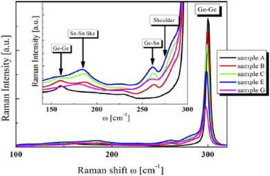
M. Oehme et al. grew GeSn layer on a relaxed Ge layer above the silicon wafer. They made a series of different GeSn thicknesses with different concentrations of Sn, as shown in the following Table 1.53 Also, they employed Raman spectroscopy to investigate the strain of the GeSn layer relative to the Ge layer underneath with increasing Sn content up to 12.5%, as shown in Fig. 11. They observed that the intensity of the Ge–Ge peak at 300 cm−1 decreases continuously with increasing Sn content, showing a shift to lower wavenumbers. In addition to this major intensive peak, another distinguished mode in the range of 250–300 cm−1 appears. The spectrum shows a peak at 262 cm−1, which is attributed to the typical GeSn mode; furthermore, a second peak at 285 cm−1 causes a shoulder in the rising edge of the Ge–Ge peak. At a lower wavenumber, a further peak at 185 cm−1 is attributed to an Sn–Sn-like mode frequency. For the investigated GeSn alloys, this vibrational mode shifts strongly (10 cm−1) with the Sn content compared to the other Raman modes. The mode appeared at 160 cm−1 is assigned to Ge–Ge vibration (Fig. 11).
Table 1 Different GeSn thicknesses with different concentrations of Sn.53
| Sample53 |
Sn content (%) |
GeSn thickness (nm) |
| A |
0 |
— |
| B |
2.4 |
261 |
| C |
4.7 |
255 |
| D |
6 |
255 |
| E |
8 |
115 |
| F |
11 |
45 |
| G |
12.5 |
34 |
 |
| | Fig. 11 Raman shifting of Ge–Ge and GeSn modes in different samples (A, B, C, E and G) with different Sn content. “Reproduced from ref. 53 with permission from [Elsevier Ltd], copyright [2013]”. | |
Table 2 summarizes the level and types of strain in different strain engineering methods and Sn contents.
Table 2 Strain level of strain engineering methods
| Group |
Method |
Strain effect |
Percentage of strain |
| Yuye Kang et al.23 |
Uniaxial compressive strain of Ge1−xSnx obtained by patterning the GeSn layer into the nanofins and relaxed with the fin width decreasing |
Relaxation of compression |
−1% |
| S. Assali et al.30 |
Growth of Ge/GeSn core/shell NW allows compressive strain relaxation and reduces the structural defects at the GeSn/Ge interface |
Relaxation of compression |
−0.7% |
| Hiroshi Oka et al.39 |
Annealing of the GeSn layer above the quartz substrate that has a high melting point. As a result of the low thermal expansion coefficient of quartz, the nucleation of GeSn at high annealing temperature is suppressed, producing tensile-strained GeSn |
Tensile strain |
Above 0.5% |
| Wei Dou et al.46 |
Sn incorporation increases the compressive strain in GeSn |
Compressive strain |
Sn content% |
Strain% |
| 9.4 |
−0.04 |
| 11.4 |
−0.14 |
| 14.4 |
−0.29 |
| 17.4 |
−0.38 |
| 19.0 |
−0.61 |
| Jérémie Chrétien et al.32 |
Tensile strained Ge bridge is formed with the aid of arms on both the sides. The strain increases with increasing arm length |
Tensile strain |
Up to 2% (250 μm arm length) |
| Anas Elbaz et al.36 |
The stressor layer surrounding the GeSn microdisk causes tensile strength in GeSn outward from the network |
Tensile strain |
1.4% |
| S. An et al.41 |
Strained flexible GeSn nanomembranes deposited on printed flexible polyethylene terephthalate (PET) |
Tensile strain |
0.44% |
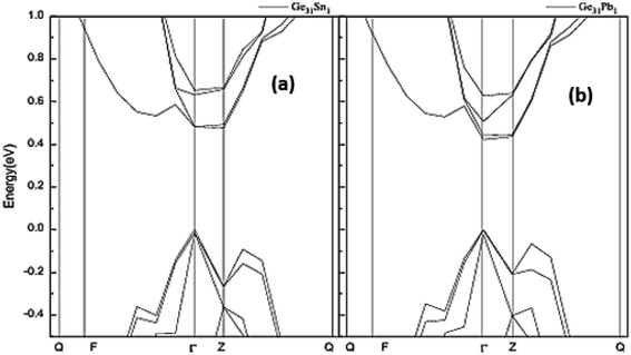
As seen above, Ge strain engineering implies that the pressure in the lattices causes distortion and orientation in the bonds of the semiconductor network. This causes many changes in the electronic wave function, and the band structure will change due to the disordering and stretching of bonds.20 Another method to convert the transition of semiconductors from direct to indirect is the alloying of semiconductor such as Ge with Pb or Sn, forming GePb or GeSn compounds or heavy doping of Ge with n-type dopants such as Sb.54 Pb-like Sn that modulates the indirect bandgap of Ge to a direct one via the lowering of the Γ valley of the Ge's conduction band by the hybridization of Ge and Sn or Pb. GeSn alloys were deposited via Ge and Sn precursors in the CVD or MBE reactor, but it is difficult to get the Pb precursor for CVD; thus, there are few trials to prepare GePb alloys. Hakimah Alahmad et al. reported that they prepared GePb by the thermal evaporation of Ge and Pb, followed by thermal annealing so that Pb diffuses by the high temperature in Ge.55 Some of the studies reported that Pb causes higher strain in Ge network than Sn. The GePb lattice constant is higher than GeSn, and the solubility of Pb is higher than Sn as it has higher electronegativity. Wenqi Huang et al. reported that the 3.125% concentration of Pb achieved direct transition compared to the same concentration of Sn in GeSn as the 6s states in Pb cause sufficient lowering of the conduction band in the GePb alloy than the 5s Sn states in the GeSn alloy56 (see Fig. 12a). Christopher A. Broderick et al. reported that Pb lowers the gap value compared to Sn with increasing Pb concentration57 (see Fig. 12b). Table 3 shows the reduction in the bandgap values and the increase in the lattice constant in Ge alloys with increasing Sn and Pb. It is seen that Pb has a higher impact on the change of the lattice constant and tuning of the bandgap value compared to Sn.
 |
| | Fig. 12 Lower conduction band states in GePb compared to the GeSn compound. “Reproduced from ref. 57 https://arxiv.org/abs/1911.05679 CC BY-NC-SA 4.0”. | |
Table 3 Lattice constants and energy gap values in terms of Sn and Sb concentrations in GeSn and GePb alloys
| Alloy57 |
Lattice constants (Å) |
Alloy |
Energy gap (eV) |
| GePb (x = 12.5%) |
6.11 |
GePb (x = 1.56%) |
0.616 |
| GeSn (x = 12.5%) |
5.65 |
GeSn (x = 1.56%) |
0.681 |
| GePb (x = 25%) |
5.90 |
GePb (x = 6.25%) |
0.020 |
| GeSn (x = 25%) |
5.76 |
GeSn (x = 6.25%) |
0.388 |
| GePb (x = 50%) |
6.22 |
— |
— |
| GeSn (x = 50%) |
5.99 |
— |
— |
The above methods show direct transition in Ge by reducing the difference between the indirect L valley and direct Γ valley of the germanium conduction band by the strain in the Ge network. Another mean was used to achieve direct transition by filling conduction electrons in indirect L valley to compensate the energy difference between both the valleys. It occurs via the heavy doping of Ge with an n-type dopant such as Sb.58 Ashkan Rajabi-Maram et al. prepared Ge doped with Sb. They found that the lattice constant of Ge–Sb reduced to 4.10 Å compared to Ge and the bandgap was slightly lowered to 0.64 eV.59
1.3. GeSn growth techniques
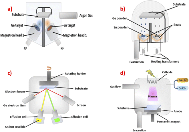
Sn has low solubility in the Ge matrix. It is only 1% below 500 °C.11 The melting point of Sn is 231 °C; thus, the raising of the temperature above 500 °C causes Sn segregation. Thus, Ge and Sn synthesis should be carried out at relatively low temperature.60 Many works have tried to fabricate the alloy of Ge and Sn at low temperature on different substrates. Haofeng Li et al. used thermal co-evaporation using two boats containing Ge and Sn (see Fig. 13b). Ge and Sn were simultaneously deposited to form amorphous GeSn with an Sn content of 4.7% with a film thickness of 150 nm.61 H. Khelidj et al. tried to prepare GeSn compound using DC magnetron co-sputtering by applying a power of 150 W from the DC power supply on the Ge target and 15 W on the Sn target (see Fig. 13a). They obtained a film of a-GeSn. Then, they annealed the prepared samples at temperature in the range from 423 to 853 K. They obtained 11% Sn content in the GeSn compound at the beginning of the annealing and then reduced to 4% by raising the temperature.62 Wei Dou et al. used plasma-enhanced chemical vapor deposition technique with different growth temperatures to grow the GeSn alloy. The GeH4 and SnCl4 precursors were inserted in the chamber with argon gas between the cathode and anode (see Fig. 13d). The formed plasma dissociated the Ge and Sn, and then bonded to each other on the substrate. They reached from 3.9 to 6% Sn content in GeSn at a temperature growth of 350 °C compared to the sample grown at 400 °C, which contains only 3% Sn content.63 Z. P. Zhang employed the molecular beam epitaxy technique to grow GeSn. They used electron gun as a source from Ge and the effusion cell from Sn in a hot crucible (see Fig. 13c). The germanium flux was 0.75 Å S−1, and they changed the flux of Sn from 0.025 to 0.6 Å S−1 for different samples to get GeSn of Sn content in the range from 3.36% up to 7.72%.64
 |
| | Fig. 13 Schematic diagram of (a) magnetron co-sputtering, (b) thermal vacuum co-evaporation, (c) molecular beam epitaxy, and (d) plasma-enhanced chemical vapor deposition for GeSn compound. | |
1.4. GeSn-based LED devices
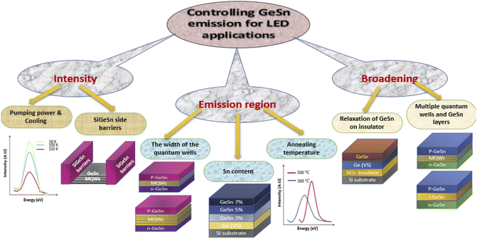
In this section, we will explore how the different structures of GeSn such as quantum wells, multilayers, and different configurations of GeSn heterostructures that influence the direct transition emission of GeSn as well as different structures of direct transition GeSn-based LED devices with controlled emission intensity and emission band of spectra in the mid-IR region of the spectrum. Controlling the bandgap is responsible for the position of the emitted spectra and, consequently, radiative and non-radiative transitions. As mentioned above, Sn incorporation in the Ge network modulates the bandgap and consequently the emission properties of GeSn compounds. Fig. 14 shows how some previous works tried to control the broadening of the GeSn emission by quantum confinement via the strain relaxation of GeSn on the insulating layer and reducing the broadening of the emission.65,66 Other experiments aimed to increase the emission band by applying different thicknesses of MQWs from GeSn67 or using different Sn content multilayers of GeSn.68 The position of the emitted spectra can also be controlled by the percentage of Sn content69 and the thickness of GeSn QWs that achieve a definite level of quantum confinement.70 The effect of growth or annealing temperature induces Sn incorporation inside the Ge network.71 The intensity of GeSn spectral emission can be enhanced through the reduction of non-radiative transitions via the temperature cooling process that freezes the charge carriers from tunneling72 and side barriers in between the confined GeSn QWs charge carriers.73
 |
| | Fig. 14 Controlling the emission properties of GeSn compound with different heterostructure configurations for LED applications. | |
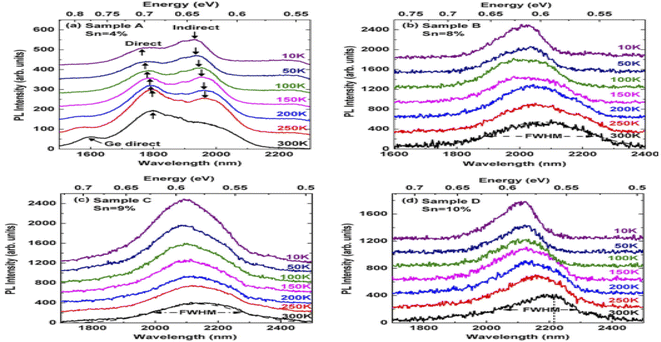
1.4.1. Direct bandgap GeSn PL via band structure manipulation. S. A. Ghetmiri et al. utilized the effect of cooling temperature and the Sn content on the bandgap of the GeSn-prepared layer and prepared a set of samples by altering the Sn content with different percentages (4, 8, 9 and 10%). They obtained two portions of direct and indirect emission with separated bands at 4% Sn content. The direct and indirect emission bands overlapped as the Sn content increased from 8% to 10% with a narrower emission band at 2200 nm with Sn content equal to 10%. The intensity of PL emission increases on cooling the temperature down to 10 K (ref. 74) (see Fig. 15). Another study75 investigated the effect of increasing Sn content that contributed to increased compressive strain and reduced charge carrier mobility, causing a decrease in the PL intensity.
 |
| | Fig. 15 PL emission of the GeSn-prepared layer with 4%, 8%, 9%, and 10% Sn content. “Reproduced from ref. 74 with permission from [American Institute of Physics], copyright no [2014]”. | |
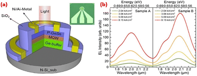
G. Grzybowsk et al. subjected the GeSn layer to the rapid thermal annealing (RTA) process to assist it to relax and then enhance the PL emission of the direct transition.76 Yuanhao Miao et al. prepared tensile strain Ge buffer layer using an eight-wafer reduced pressure chemical vapor deposition system, followed by tensile-strained GeSn layer to reduce the chance of indirect transition and increase the direct one.77 Z. Kong et al. tried to increase the tensile strain and relax the compressive strain caused by the Sn content by surrounding the GeSn with an insulating stressor layer. They prepared the GeSn layer on the Ge/Si virtual substrate and capped it by Al2O3. SiO2 layer on Si substrate, and then stacked the Al2O3 layer by diffusion bonding and Ge was etched, forming GeSn on the insulator (GeSnOI). They found that the PL peak shifted toward short wavelengths due to the relaxation of compressive strain, which lowers the direct valley of the conduction band.78 M. Grydlik et al. used the quantum dot structure of Ge to obtain broadband emission of Ge. They deposited a 0.6 nm layer of Ge, forming quantum dots, and bombarded them in crystalline silicon. They obtained broad emission from 1300 nm to 1600 nm, which increased in terms of the cooling temperature.79 Linzhi Peng et al. attempted to obtain broadband GeSn emission via the fabrication of multi quantum wells (MQWs) with different Sn content for each well. A Ge bottom layer of 250 nm was grown at 300 and 600 °C for the two samples as a virtual substrate and for four quantum wells grown at 200 °C. The quantum well was composed of 10 nm thick of Ge1−xSnx (sample A with 7.3% and sample B with 8.5% Sn content) separated by 20 nm Si0.1Ge0.85Sn0.05 barrier layer, then a 120 nm thick B-doped Ge0.95Sn0.05 as a capping layer on the MQWs, as shown in Fig. 16a.80 The EL spectra of the two samples consists of two main peaks. The EL peak shown in Fig. 16b is at a wavelength of 1980 nm, and another low intensity peak is at 1850 nm. For sample B, these two peaks are at 2060 nm and 1850 nm, respectively. In these two samples, the high-energy peaks are attributed to the emission of GeSn QWs, and the low-energy peaks are attributed to the Ge-buffer layer that allows their application in light emission within the NIR region.81,82
 |
| | Fig. 16 MQWs grown between Ge BL and p-GeSn cap and the PL spectra at different pump power densities. “Reproduced from ref. 80 with permission from [Elsevier Ltd], copyright [2020]”. | |
Another heterostructure composed of quantum wells with bottom and top barriers that differ in the Sn content than the well-constructed were demonstrated by Perry C. Grant et al.83 The design of the structure is as follows: a bottom barrier Ge0.915Sn0.085 of 412 nm-thickness, 11 nm Ge0.863Sn0.137 quantum well, and 47 nm Ge0.927Sn0.073 top barrier is shown in Fig. 17a, which serve as an LED in the mid-IR region. PL measurements show a major peak at 2200 nm, which is attributed to the indirect transition of GeSn and a small peak at 2500 nm is attributed to the direct transition observed at 300 K. The intensity of the peak at 2500 nm increases with the decrease in the temperature, while the 2200 nm peak decreases as the temperature decreases, as shown in Fig. 17b. This is because the cooling temperature compensates the difference in the energy between the direct and indirect valleys.84
 |
| | Fig. 17 Quantum well with bottom and top barriers and direct bandgap emission at different temperatures. “Reproduced from ref. 83 https://aip.scitation.org/doi/full/10.1063/1.5020035 CC BY 4.0”. | |
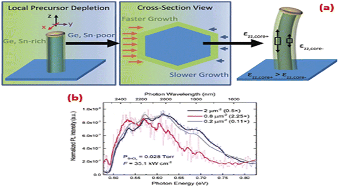
Andrew C. Meng et al. obtained broad emission by growing Ge/GeSn core cladding nanowires. Germanium nanowires were grown via a two-step vapor–liquid–solid (VLS) process using a nucleation step at 375 °C, followed by steady-state growth at 300 °C, as shown in Fig. 18a. The samples exhibited PL emission at wavelengths longer than 2400 nm, which is not detected by the used detector.85 The PL has higher energy photon emission due to the low Sn content regions in nanowires in the size range between 1700 and above 2400 nm, as illustrated in Fig. 18b.
 |
| | Fig. 18 Ge/GeSn core cladding nanowires and emission characteristics. “Reproduced from ref. 85 with permission from [Royal Society of Chemistry publisher], copyright [2021]”. | |
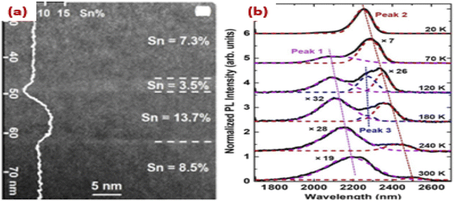
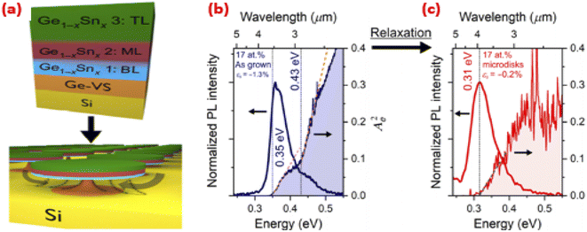
Ge1−xSnx multilayer heterostructure was prepared by S. Assali et al. with different thicknesses and Sn compositions. A 600–700 nm Ge-VS was grown at 450 °C. The incorporation of Sn was controlled by the growth temperature. The Ge1−xSnx multilayer heterostructure consisted of 17 at% top layer (TL), 12–10 at% middle layer (ML), and 8 at% bottom layer (BL) grown at 280, 300, and 320 °C, with thicknesses of 160, 155, and 65 nm, respectively, as seen in Fig. 19a. The main PL peak appearing from the 17 at% TL was at 0.365 eV with an FWHM of 40–50 meV.86 A low-intensity emission peak detected at approximately 0.43 eV is attributed to the radiative recombination in the underlying 12 at% middle layer (see Fig. 19b).
 |
| | Fig. 19 Ge1−xSnx multilayer with different Sn content heterostructures and its PL emission. “Reproduced from ref. 86 with permission from [American Physical Society publisher], copyright [2021]”. | |
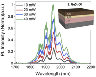
Daniel Burt et al. employed the relaxation of strained GeSn on the SiO2 insulating layer, causing the shrinkage of the bandgap. A 200 nm Ge0.94Sn0.06 layer was grown on the insulating oxide layer (shown in Fig. 20), followed by a 1000 nm Ge buffer layer on Si wafer using low-pressure CVD. The insulating layer was made of thermal oxide with a thickness of 1 μm grown on an Si wafer, followed by a 150 nm Al2O3 layer deposited at 250 °C and annealed at 350 °C in a tube furnace under nitrogen gas. The PL measurements shows different continuous peaks ranging from 1800 nm to 2100 nm.87
 |
| | Fig. 20 Ge0.94Sn0.06 layer was grown on the insulating oxide layer and the PL emission at different pumping powers. “Reproduced from ref. 87 https://opg.optica.org/oe/fulltext.cfm?uri=oe-29-18-28959%26id=458147 CC BY 4.0”. | |
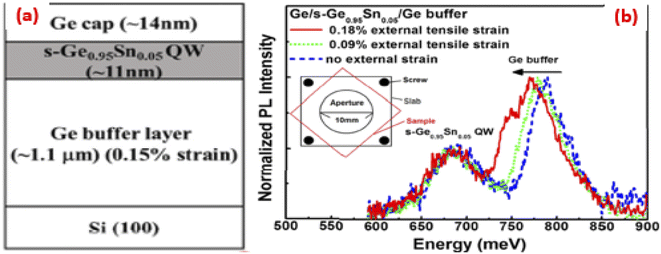
Chung-Yi lin et al. fabricated a heterostructure with multiple QWs sandwiched between the cap and buffer Ge. A 11 nm GeSn quantum well was sandwiched between 1.1 μm Ge buffer and the 14 nm Ge cap on the Si substrate, as shown in Fig. 21a. The PL spectra of the prepared structure showed broad peaks at 0.67 eV and 0.78 eV, which were attributed to the Ge buffer and GeSn QW, respectively,88 which is tensile strained, as shown in Fig. 21b.
 |
| | Fig. 21 GeSn quantum well sandwiched between the Ge buffer and the Ge cap on Si substrate and its PL emission. “Reproduced from ref. 88 https://opg.optica.org/ome/fulltext.cfm?uri=ome-8-9-2795%<?pdb_no 26id?>26id<?pdb END?>=396351 CC BY 4.0”. | |
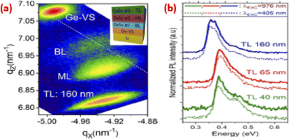
S. Assali et al. investigated the effect of different thicknesses of the GeSn layers on the control of the position of the spectral peaks to control the region of emission of GeSn-based LEDs. They grew multi-layered GeSn heterostructure on a 650 nm Ge/Si virtual substrate, as shown in Fig. 22a. Sn incorporation was controlled at 320 °C, 300 °C, and 280 °C growth temperatures for the BL, ML, and TL, respectively. The thickness of TL was controlled by changing the growth time in the range from 24 to 120 minutes, leading to a TL thickness in the 40–160 nm range. A sharp main emission peak was detected at 0.39 eV for the 16.46 at% Sn content samples with a TL of thickness 40–65 nm. There is another shoulder peak detected at 0.43–0.44 eV. As the thickness of the top layer increases to 160 nm, it induces a red shift for both the peaks to 0.36 eV and 0.41 eV.89 The FWHM for the main emission at 0.36–0.39 eV is only 30–50 meV, as shown in Fig. 22b. With the application of atom probe tomography, it revealed the presence of various abrupt interfaces between the monocrystalline GeSn layers with interfacial widths in the 1.5–2.5 nm range. Statistical analyses of 3-D atom-by-atom maps confirmed the absence of Sn precipitates and short-range atomic ordering. This work opens the door to the development of mid-infrared photonic devices from silicon-compatible compounds.
 |
| | Fig. 22 Multi-layered of GeSn heterostructure on Ge/Si virtual substrate (VS) and EL spectra as a function of TL thickness. “Reproduced from ref. 89 with permission from [American Institute of Physics publisher], copyright [2018]”. | |
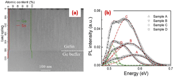
Tao Liu et al. tuned the position of the spectral emission peak by adjusting the Sn content in the GeSn compound. They prepared samples of GeSn compound labeled as A, B, C, D, and E with Sn contents of 1.2, 2.9, 3.9, 5.0, and 7.4 at%, respectively. The samples were grown on Ge substrates via the MBE system. The thermal annealing at 440 °C for 5 min was used to remove the oxidation layer on the surface. The heterostructure of GeSn consisted of a 100 nm Ge buffer layer deposited at 400 °C, followed by 500 nm films of Sn content varying from 1.2 to 7.4%, which were deposited for the mentioned samples, as shown in Fig. 23a. The crystal quality of the GeSn films was improved by thermal annealing at 520 °C for 5 min.66 For sample E with the highest Sn content of 7.4%, there are no detected PL signals even after annealing. All the PL spectra was attributed to the two peaks labeled 1 and 2 for the A–D samples, as shown in Fig. 23b. The fitted peak is at 0.6 eV for sample A having low Sn content and the redshifted one is at 0.52 eV for higher Sn content in D sample.90–92
 |
| | Fig. 23 GeSn film samples corresponding to the Sn contents and their PL emission. Reproduced from ref. 90 with permission from [IOPscience publisher], copyright [2018]”. | |
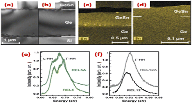
Heterostructures of GeSn with different Sn contents, followed by Ge buffer on Si substrate, were fabricated by P. Zaumseil et al. and are shown in Fig. 24a–d. They minimized lattice constant mismatch between GeSn-grown BLs. Three samples labeled REL5, REL9, and REL12, with Sn 5, 9, and 12 at% compositions were grown by controlling the growth temperature in the range of 350–400 °C.93 They employed the annealing temperature to shift the peak position. They made a comparison between the PL characteristics of REL5 and its annealed counterpart labeled REL5A. Both samples have slightly indirect transition with PL spectrum with two dominant emission peaks at about 0.7 eV and 0.67 eV. In the annealed REL5A sample, they observed that the spectral intensity of the direct transition is more dominant and red-shifted, and the PL FWHM is reduced from 82 meV to 67 meV (Fig. 24e and f). This confirms the increased plastic relaxation because of the annealing effect.94,95 The REL12A sample only shows a narrowing at about 0.53 eV and an increase in the intensity of the emission line, but the peak shift is negligible.
 |
| | Fig. 24 Heterostructures with different Sn content of GeSn in Ge buffer on Si substrate and PL emission as a function of annealing temperature. “Reproduced from ref. 93 https://aip.scitation.org/doi/full/10.1063/1.5036728 CC BY 4.0”. | |
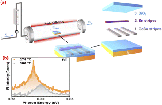
Another study by Lu Zhang et al. employed the annealing temperature to control the position of the emission peak. They fabricated amorphous GeSn strips of dimensions 3.6 μm width, 200 μm length, and 50 nm thickness patterned on Si-based substrates using photolithography and reactive etching magnetron sputtering, respectively. Sn and Ge were co-sputtered for the deposition of GeSn in Ar reactive ions, as shown in Fig. 25a. The Sn content of 2% for a-GeSn was controlled by adjusting the sputtering power ratio on the Sn and Ge targets. Next, perpendicular 4.3 μm width Sn strips were deposited on the top of the a-GeSn. These strips were covered by a 500 nm SiO2 layer deposited by the PE-CVD technique. The samples were finally annealed at 275 and 300 °C for 40 h in N2 environment. Fig. 25b shows the RT photoluminescence of the samples annealed at 275 and 300 °C. The peak of the samples annealed at 275 °C appeared at 0.787 eV, which shifts to 0.8 eV for samples annealed at 300 °C.96
 |
| | Fig. 25 Sn strips orthogonal to GeSn strips and PL emission at different growth temperatures. “Reproduced from ref. 96 with permission from [Elsevier Ltd], copyright [2022]”. | |
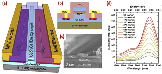
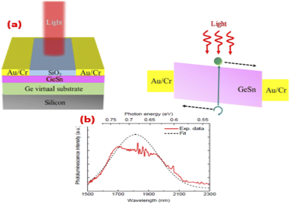
A dominant method to enhance the emission intensity of GeSn-based LEDs is to reduce the non-radiative transitions. Linzhi Peng et al. used a side barrier to reduce the non-radiative transition of the charge carriers. They grew lateral Ge1−xSnx/Ge MQW samples on Ge buffer/Si (100) substrate via molecular beam epitaxy (MBE). The designed MQW structures were formed from a Ge-buffer layer with a thickness of 500 nm by two-step growth, forming a 70 nm thick Ge buffer layer at a temperature of 300 °C, covered by a 430 nm thick layer of Ge grown at 600 °C.97 Five quantum wells were grown of the composition 10 nm thick Ge0.91Sn0.09 well layers at 190 °C separated by 20 nm Ge barrier layers sandwiched between 150 nm thick n- and p-type Ge-cap layer to prevent Sn segregation in the GeSn layer,98,99 as illustrated in Fig. 26a–c. A rapid cyclic annealing at 600–800 °C was done five times to decrease lattice constant mismatch under the MQWs structure.100,101 The EL spectra of the Ge0.91Sn0.09/Ge MQW p–i–n LED is shown in Fig. 26d. A high intensity peak at 2160 nm with FWHM of 210 nm was observed. As a result of the carrier's recombination in a tensely strained Ge-base and Ge capping layer, a low intensity peak was detected at 1900 nm. Soumava Ghosh et al. fabricated a device based on GeSn. The layer structure consisted of a GeSn active layer as the absorption layer grown on the Si substrate via Ge virtual substrate (VS) with a passivated surface by SiO2, as shown in Fig. 27a.102 GeSn active region enhances the absorption of the pure Ge due to the low energy direct bandgap and hence larger absorption coefficient.103–105 The GeSn PL emissions were detected using FTIR spectroscopy. The emission was in the range of 1700–1900 nm and the emission peak was observed at 1800 nm, as shown in Fig. 27b.
 |
| | Fig. 26 Lateral Ge1−xSnx/Ge MQW samples grown on the Ge buffer/Si (100) substrate and PL emission at different power densities. “Reproduced from ref. 97 https://opg.optica.org/prj/fulltext.cfm?uri=prj-8-6-899%26id=432022 CC BY 4.0”. | |
 |
| | Fig. 27 GeSn on Ge virtual substrate (VS) with a passivated surface by SiO2 and PL emission. “Reproduced from ref. 102 https://www.mdpi.com/2072-<?pdb_no 666X?>666X<?pdb END?>/11/9/795 CC BY 4.0”. | |
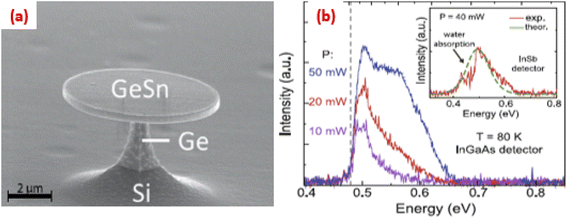
Denis Rainko et al. utilized different pump powers to increase the emission intensity of the optically pumped GeSn heterostructures. They studied the influence of tensile strain of a stressor layer-covered a microdisk of GeSn on the optical properties of the heterostructure. They grew a Ge0.94Sn0.06 layer on the top of a Ge-VS. A 265 nm GeSn layer was grown at a temperature of 375 °C with −0.32% biaxial compressive strain. This is done by the influence of the strain from an SiNx stressor on a microdisk surface.106 The microdisks of GeSn cavities were then patterned using electron beam lithography, as shown in Fig. 28a. The measured PL measurements illustrated both direct bandgap transitions with an energy value of 0.56 eV and indirect bandgap transitions with an energy value above 0.62 eV (Fig. 28b), and the intensity increases with increasing pumping power.
 |
| | Fig. 28 A microdisk of GeSn covered by the stressor layer and PL emission with different pumping powers. “Reproduced from ref. 106 https://www.nature.com/articles/s41598-018-36837-8 CC BY 4.0”. | |
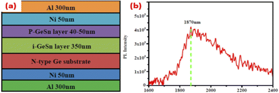
1.4.2. Direct bandgap GeSn LEDs. Through this section, we will review the different structures of GeSn-based LEDs with controlled emission. J. Yang et al. prepared a heterostructured device of doped and undoped GeSn multilayers. They grew 350 nm i-GeSn layer, followed by 40–50 nm p-GeSn on n-type Ge substrate, forming a p–i–n diode of different GeSn thicknesses using the sputtering technique,107 as shown in Fig. 29a. The PL emission of GeSn was broad and located at about 1870 nm (Fig. 29b). They compared the PL peak position of GeSn with the results of another work and found that it is smaller than that of a direct bandgap GeSn with a 2230 nm PL peak. From the HR-XRD result, the relaxation degree of the GeSn layer was evaluated to be approximately 50%. Therefore, they concluded that the GeSn layer is an indirect bandgap material. It may be attributed to the large lattice mismatch between Ge and GeSn (the lattice constant of GeSn is larger than Ge), which indicates that the GeSn layer is under compressive strain and is averse to the bandgap transformation of Ge from indirect GeSn material to direct GeSn material.
 |
| | Fig. 29 p-Ge/i-GeSn/n-Ge p–i–n diode and its PL emission. “Reproduced from ref. 107 https://www.mdpi.com/1996-1944/12/17/2662 CC BY 4.0”. | |
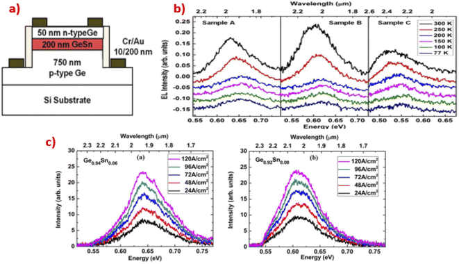
Y. Zhou et al. deposited 200 nm GeSn layer with different Sn contents (6.06, 6.44, 9.24%) sandwiched between 750 nm p-Ge and 50 nm n-Ge cap to prepare a set of p–i–n diodes (see Fig. 30a) labeled as A, B, and C. The EL measurements revealed that device B has higher emission than C, which has a higher content of Sn, causing high compressive strain and a reduction in the mobility of charge carriers and the emission intensity. The increasing intensity can be controlled by the cooling temperature. The emission peak shifts toward longer wavelengths as the Sn content increases, as seen in Fig. 30b.108 The same group tried another study with only 6 and 8% Sn content in the same diode structure. They obtained the same conclusion related to the impact of Sn content, and they studied the increasing emission intensity in terms of pumping power intensity, as shown in Fig. 30c.109
 |
| | Fig. 30 (a) GeSn ridge-based p–i–n diode, (b) PL emission of the prepared set of diodes as a function of cooling temperature, PL emission of 6% and 8% GeSn-based fabricated diodes as a function of pumping power intensity. “Reproduced from ref. 108 with permission from [American Institute of Physics publisher], copyright [2016]”. | |
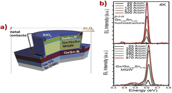
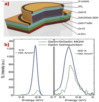
D. Stange et al. used the multi quantum well structure sandwiched between p-type germanium buffer and n-type GeSn cap. Ge/GeSn MQWs consisted of 20 nm GeSn well with 8% Sn content separated by 14 nm Ge barriers. They fabricated the p–i–n diode, as shown in Fig. 31a, with two structures (homojunction and MQWs). The EL emission showed that the homojunction and MQWs-based diodes had significant intensity emission. It was found that the peak of the emission for MQWs shifted toward higher energy due to the carrier confinement effect of the potential wells, and the peak FWHM for the MQWs-based diode was narrower,110 as seen in Fig. 31b. They undertook another study with the same homojunction structure and MQWs, except the wells consist of GeSn wells separated by the ternary higher energy bandgap SiGeSn, as seen in Fig. 32a. SiGeSn caused higher charge carriers confinement inside the GeSn well that causes significant emission for MQWs-based diode than the homojunction one,111 as seen in Fig. 32b.
 |
| | Fig. 31 (a) Schematic diagram of the prepared Ge/GeSn MQWs-based diode, (b) EL spectra of the prepared MQWs-based diode as a function of the pumping power intensity. “Reproduced from ref. 110 https://opg.optica.org/oe/fulltext.cfm?uri=oe-24-2-1358%<?pdb_no 26id?>26id<?pdb END?>=335594 CC BY 4.0”. | |
 |
| | Fig. 32 (a) Schematic diagram of the prepared Ge/SiGeSn MQWs-based diode, (b) EL spectra of the prepared MQWs-based diode at different operating temperatures. “Reproduced from ref. 111 https://opg.optica.org/optica/fulltext.cfm?uri=optica-4-2-185%26id=357781 CC BY 4.0”. | |
1.5. GeSn-based laser
1.5.1. Random lasing versus regular lasing. Lasing in an active medium requires reaching the threshold gain in that media so that the population of the higher level duplicated after that spontaneous relaxation generates photons that stimulate electrons to decay and emit an intense sharp line.112,113 There are two mechanisms of lasing for this stimulated emission. The first one is random lasing, in which the spontaneously emitted photons are scattered between the particles composing the material and stimulates the excited electrons in higher lasing levels to decay before the decay lifetime,114–117 as shown in Fig. 33a. The produced emission is in the form of lasing spikes at different wavelengths due to the randomness and the missing of coherency as the electrons do not decay at the same time with the same phase.118,119 The second mechanism is regular lasing. This mechanism requires an optical cavity consisting of two mirrors with full beam reflectivity and the other is partial reflectivity that is capable of reflecting the spontaneously emitted photons inside the active media again to stimulate the electrons in higher states to decay before the transition lifetime,120–122 as shown in Fig. 33b. These electrons decay at the same time and coherently exit from the cavity with the same phase in one direction. The emission appears as a very intense sharp main line because of the temporal coherent emitted photons.123,124
 |
| | Fig. 33 Random lasing versus regular lasing illustration. | |
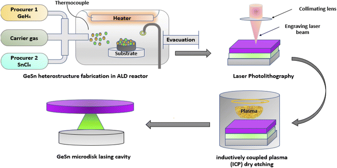
 |
| | Fig. 34 GeSn microdisks (MDs) fabrication by photolithography for achieving the stimulated emission. | |
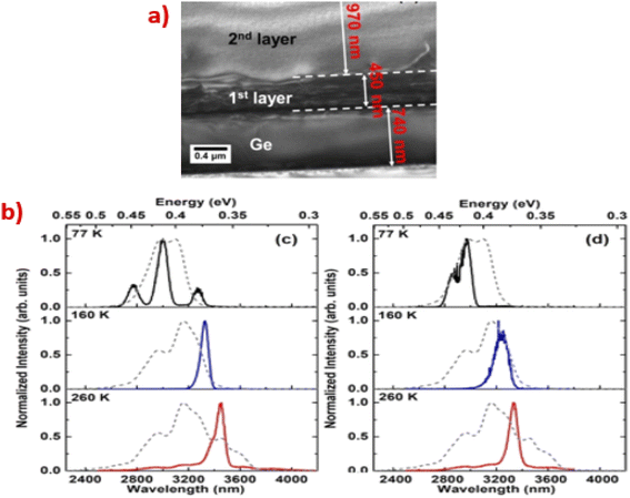
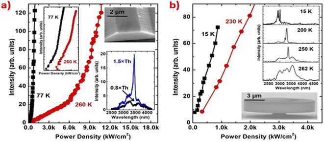
1.5.2. Optically pumped lasing. Many researchers reported lasing emission based on GeSn heterostructures.129,130 They investigated the threshold lasing pump powers and active medium cooling for line sharpness control.131,132 The impact of Sn content on the lasing line position has also been studied.133,134 In this section, we will show some studies on the lasing modes from GeSn nanolayers and the parameters on which the lasing line depends, such as the cooling temperature, Sn content percentage, and optical pump power. Many works demonstrated the reduction of dislocations in GeSn materials and carrier confinement. Yiyin Zhou et al. prepared a set of ridge waveguides with different widths and planar waveguides. They used epitaxial relaxation to reduce the dislocations due to the Sn content. They deposited 450 nm of first layer of GeSn with Sn content 11–15%, followed by 970 nm GeSn with Sn content 15–20% on low defect Ge buffer, as seen in Fig. 35a. They obtained lasing lines at 3444 nm and 4333 nm when they reached the pumping threshold density of value 6055 kW cm−2 and 9587 kW cm−2 at an operating temperature of 260 K for 100 μm width of ridge waveguide and planar waveguide (see Fig. 35b), respectively.135 Another study of the same group in which they prepare the same layers with the same Sn content except the prepared microdisk with a diameter of 10 μm to reduce the interface between the Ge buffer and the GeSn layer; hence, the dislocations were reduced. They obtained a lasing line at 3400 nm when they reached the pumping threshold density of 108 kW cm−2 at an operating temperature of 15 K compared to the ridge structure, as shown in Fig. 36a and b.136 The heterostructure of the five GeSn layers with Sn content of 14.1%, 16.1%, 17.2%, 16.1%, and 14.1% with a total thickness of 900 nm was prepared by J. Chretien to relax the upper layers of GeSn. The prepared heterostructure was etched to form 8 μm diameter of the microdisk (Fig. 37a). They obtained a 3512 nm lasing line with a pumping threshold density of 3270 kW cm−2 at 305 K (see Fig. 37b).137
 |
| | Fig. 35 (a) Cross-sectional TEM image of the prepared GeSn-based waveguide. (b) PL emission of the prepared waveguides as a function of operating temperatures. “Reproduced from ref. 135 with permission from [American Chemical Society], copyright [2017]”. | |
 |
| | Fig. 36 Emission intensity of (a) ridge, (b) microdisk of the prepared GeSn-based waveguides in terms of pumping power density. “Reproduced from ref. 136 https://www.frontiersin.org/articles/10.3389/fphy.2019.00147/full CC BY 4.0”. | |
 |
| | Fig. 37 (a) Schematic diagram of the prepared GeSn MD based on different contents of the Sn GeSn heterostructure, (b) lasing emission of the MD as a function of the pumping power. “Reproduced from ref. 137 with permission from [American Institute of Physics publisher], copyright [2022]”. | |
Anas ElBaz et al. deposited the GeSn layer with 5.4% Sn content. They employed E-lithography to fabricate 9 μm of a microdisk, then surrounded it by a 350 nm SiNx stressor layer to relax the GeSn layer and reduce dislocations. They detected 2500 nm lasing line at 45 K with a pumping threshold density of 1.1 kW cm−2.36 Hyo-Jun Joo et al. prepared 550 nm thick, 10.6% Sn content GeSn layer deposited on Al2O3 and SiO2 insulating layers on Si, then the Al2O3 layer was selectively etched so that GeSn is on SiO2, which serves in optical confinement and enhances the GeSn emission threshold. They obtained 2204 nm lasing line with a pumping threshold density of 18.2 kW cm−2 at 4 K.138 Youngmin Kim et al. prepared a p–i–n heterostructure of 3 GeSn layers with 5–7–5% Sn content deposited on 130 and 200 nm buffer GeSn layers on Ge above the Si substrate, then the Ge buffer was selectively etched so that 11 μm diameter microdisk was directly stacked on Si. A 2215 nm lasing line was detected at 4 K with a pumping threshold power equal to 60 kW cm−2.139 Bibin Wang et al. deposited 500 nm-thick GeSn with 10.5% Sn content on the SiN stressor layer above the Al heat sink layer. Another SiN stressor layer on Si was stacked on the GeSn layer. The GeSn layer was confined between two stressor layers that act as barriers for the confinement of carriers to enhance the GeSn emission. When they reached a pump threshold density of 20 kW cm−2 at 75 K, they obtained a 2340 nm lasing line.140 Yongduck Jung et al. deposited 960 nm GeSn with 10% Sn content by relaxed growth deposition on Al2O3, followed by SiO2 on Si. Then, Al2O3 was selectively etched so that GeSn was stacked on SiO2. Then, the microdisk was made by E-lithography, followed by dry etching. They obtained 2330 nm lasing line at a lower threshold pumping density of 17 kW cm−2 at 4 K.141 The following table (Table 4) summarizes the threshold value of different wavelengths of the lasing line with different Sn contents affected by the carrier confinement and the relaxation of the GeSn layers, thus reducing their dislocation to enhance GeSn emission.
Table 4 Threshold value of different wavelengths of the lasing line with different Sn contents affected by carrier confinement and the relaxation of GeSn layers
| Group |
Structure |
Max. Sn content (%) |
Lasing wavelength (nm) |
Operating temperature (K) |
Pumping power threshold density (kW cm−2) |
| Yiyin Zhou et al.135 |
Planar and ridge waveguides (450 nm of first layer of GeSn with Sn content 11–15%, followed by 970 nm of GeSn with Sn content 15–20% on low defect Ge buffer) |
20% |
3444 (ridge 100 μm), 3334 (planar) |
260 |
6055 (ridge), 9587 |
| Wei du et al.136 |
The same as the above grown layers then they etched to form 2 μm width ridge and 10 μm diameter of the microdisk |
20% |
3500 at 260 K (ridge), 3400 at 250 K (MD) |
260 (ridge), 15 (MD) |
6055 (ridge), 108 (MD) |
| J. Chrétien et al.137 |
Heterostructure of five GeSn layers of Sn content 14.1%, 16.1%, 17.2%, 16.1%, and 14.1%, respectively, with total thickness 900 nm was etched to form 8 μm diameter of the microdisk |
17.2% |
3512 |
305 |
3270 |
| Anas ElBaz et al.36 |
GeSn layer with 5.4% Sn content etched to form 9 μm MD surrounded by 350 nm of SiNx stressor layer to relax the compressed GeSn and achieve tensile strain |
5.4% |
2500 |
45 |
1.1 |
| Hyo-Jun Joo et al.138 |
550 nm-thick GeSn layer deposited on Al2O3 and SiO2 insulating layers on Si; then, the Al2O3 layer was selectively etched so that GeSn is on SiO2 |
10.6% |
2204 |
4 |
18.2 |
| Youngmin Kim et al.139 |
The p–i–n heterostructure of 3 GeSn layers with 5–7–5% of Sn content were deposited on 130 and 200 nm buffer GeSn layers on Ge above the Si substrate; then, the Ge buffer was selectively etched so that 11 μm diameter microdisk was directly stacked on Si |
7% |
2215 |
4 |
60 |
| Binbin Wang et al.140 |
500 nm-thick GeSn with 10.5% Sn content was deposited on the SiN stressor layer above the Al heat sink layer. Another SiN stressor layer on Si stacked on the GeSn layer for optical confinement |
10.5% |
≃2340 |
75 |
20 |
| Yongduck Jung et al.141 |
960 nm GeSn with 10% Sn content by relaxed growth deposition on Al2O3, followed by SiO2 on Si. Then, Al2O3 was selectively etched so that GeSn was stacked on SiO2. Then, the microdisk is prepared by E-lithography, followed by dry etching |
10% |
≃2330 |
4 |
17 |
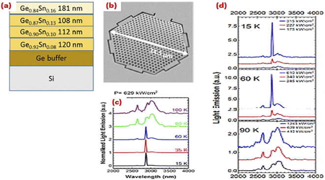
1.5.2.1 controlling the broadening and intensity of the lasing line via cooling temperature. Q. M. Thai et al. reported the lasing action in the 2D hexagonal photonic crystals fabricated from the Ge0.84Sn0.16 layer deposited by RP-CVD and investigated the line sharpening and intensity at range of temperature from 15 to 100 K. The GeSn active layer was deposited on Ge buffer layer above the Si (001) substrate. A 380 nm active layer was fabricated from 16% Sn containing GeSn layer of thickness 181 nm, 108 nm of 13% Sn containing GeSn layer, and 10% Sn containing GeSn layer of thickness 91 nm, as shown in Fig. 38a and b. Step-graded Sn content GeSn layer was fabricated by the decrease in the temperature during the deposition process till the Sn content reached 16 at%. Electron beam photolithography was used to engrave the Ge/GeSn stack, followed by selective CF4 dry-etching and reactive-etching O2 plasma. Lasing emission was characterized under a threshold high density power of 629 kW cm−2 at different operating temperatures in the range of 15–100 K. Fig. 38c and d shows the change in the PL emission spectra in terms of the temperature variance. A sharp lasing emission was obtained at a temperature up to 60 K. If the temperature increases above this value, only the spontaneous PL emission of the membrane was detected.142 The figure shows three lasing lines at 15, 60, and 90 K for different pumping densities. At low pumping densities, they observed only spontaneous PL emission with broad and low intensity.143,144 The lasing occurred at a lasing pump threshold (227 kW cm−2 and 340 kW cm−2 at 15 K and 60 K, respectively). The spectral intensity around the lasing peak is in the range of 2700–2910 nm.
 |
| | Fig. 38 Lasing in 2D hexagonal photonic crystals fabricated from the Ge0.84Sn0.16 layer. “Reproduced from ref. 142 with permission from [American Institute of Physics publisher], copyright [2018]”. | |
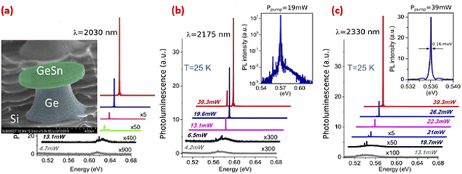
MQWs GeSn stacked between SiGeSn barrier heterostructures were grown by Daniela Stange et al. in a reduced pressure chemical vapor deposition reactor.145 All heterostructures were grown on Ge-buffered 200 μm Si(001) wafers. A 200 nm thick, relaxed Ge0.9Sn0.1 layer was used as a buffer layer to achieve lattice mismatch between the Ge-VS and the GeSn/SiGeSn stacks on the top.146 The incorporation of Sn inside the SiGeSn barriers was controlled by the growth temperature of about 300 °C. Microdisk cavities were fabricated using photolithography.147–150 The PL spectra of MQW were obtained at different temperatures, pumping with a laser of wavelength 1064 nm. A 72 kW cm−2 peak pump power achieve dominant lasing emission at 495 meV. The lasing line became narrower from 18 meV at a pumping power of 27 kW cm−2 to 2.9 meV at a pump power of 125 kW cm−2 as the temperature decreased and the pumping power increased. A very sharp lasing spectrum was detected at 20 K with 1550 nm wavelength optical pumping of 187 kW cm−2 power density at 0.5 eV with (FWHM) in the range between 0.65 and 1 meV. (a) Controlling the GeSn line position in terms of the Sn content. Anas Elbaz et al. employed Sn content adjustment in GeSn lasing line position controlling. They fabricated GeSn microdisk cavities with various Sn contents of 7, 8.1, and 10.5% on Ge virtual substrate above the Si base substrate using photolithography processes. The microdisk diameters ranged from 4 to 10 μm. All microdisks were under-etched to 1.5 μm from the edges, forming a very narrow Ge pillar in the center of the disks. PL measurements were performed at 25 K for each microdisks with different Sn content. They obtained laser emission at a pumping threshold, as seen in Fig. 39a. Above this threshold, a single lasing mode appeared on the background emission. The line width of the lasing beam was 100 meV.151 The lasing lines were 2030 nm, 2175 nm, and 2330 nm for 7, 8.1, and 10.5% samples, respectively, as seen in Fig. 39a–c.
 |
| | Fig. 39 The lasing characteristics of different Sn content GeSn microdisks. “Reproduced from ref. 151 with permission from [American Chemical Society publisher], copyright [2020]”. | |
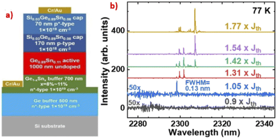
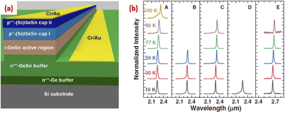
1.5.3. Electrically pumped lasing. Most works investigated the lasing action in the optically pumped GeSn lasing media. Few studies reported the electrical injection of the GeSn lasing media. Yiyin Zhou et al. fabricated different lengths of 80 μm width ridge waveguide laser consisting of 500 nm n-Ge buffer, 700 nm of relaxed n-GeSn starting with 8% Sn content to 11% of Sn content on the top, then 1000 nm of intrinsic GeSn, followed by p-type Si0.03Ge0.89Sn0.08 of thickness 170 nm, followed by another layer of the same composition with a thickness of 70 nm for electron confinement (see Fig. 40a). The electrodes are made of Cr/Au. They got lasing spikes with a main line at 2300 nm with a peak width equal to 0.13 nm at a threshold of 598 A cm−2 for electrical pumping (Fig. 40b).152
 |
| | Fig. 40 (a) 80 μm width ridge waveguide laser structure, (b) electrically injected lasing line characteristics of the prepared ridge waveguide laser. “Reproduced from ref. 152 https://opg.optica.org/optica/fulltext.cfm?uri=optica-7-8-924%26id=434176 CC BY 4.0”. | |
This group reported another study of the same structured ridge waveguide laser changed the Sn content in the active layer and layers thicknesses of the p-SiGeSn cap to control the lasing threshold and lasing line position in a series of five samples. The samples' Sn content in the active layer and layer thicknesses of the p-SiGeSn cap are summarized in the following table. The SiGeSn cap layer with p-type dopant (boron) with 50 nm thickness covered the prepared heterostructures (see Fig. 41a). The GeSn buffer layers have different Sn contents of 7% to 11% and are labeled by samples A to D and 10% to 13% in sample E, as shown in Table 5. The GeSn active region had 11% Sn content in samples A to D and 13% of Sn content in sample E. They obtained a lasing line for the 190 nm SiGeSn-cap device at a threshold of 0.6 kA cm−2 at 10 K compared to 1.4 kA cm−2 of the 150 nm SiGeSn-cap device. The 220 nm GeSn-cap device showed threshold at 2.4 kA cm−2. The lasing line position was altered in terms of the Sn content in the active layer of the samples, as shown in Fig. 41b. The following table shows the corresponding lasing line position and its threshold for each sample.153
 |
| | Fig. 41 SiGeSn p–i–n waveguides and lasing characteristics. “Reproduced from ref. 153 https://opg.optica.org/prj/fulltext.cfm?uri=prj-10-1-222%26id=466197 CC BY 4.0”. | |
Table 5 Summary of Laser Structures with different Sn contents and thicknesses.153
| Sample |
p-Type cap |
GeSn active region |
n-Type buffer |
Threshold at 10 K (kA cm−2) |
Lasing wavelength at 10 K (nm) |
| Material |
Thickness (nm) |
Sn content% |
Thickness (nm) |
Material |
Thickness (nm) |
| A |
Si0.03Ge0.89Sn0.08 |
190 |
11.2 |
610 |
Ge0.93Sn0.07 |
950 |
0.6 |
2238 |
| B |
Si0.03Ge0.89Sn0.08 |
150 |
10.8 |
430 |
Ge0.93Sn0.07 |
670 |
1.4 |
2281 |
| C |
Ge0.95Sn0.05 |
220 |
11.2 |
520 |
Ge0.93Sn0.07 |
650 |
2.4 |
2294 |
| D |
Ge0.95Sn0.05 |
100 |
11.5 |
450 |
Ge0.93Sn0.07 |
610 |
3.4 |
2272 |
| E |
Si0.03Ge0.89Sn0.08 |
180 |
13.1 |
540 |
Ge0.93Sn0.07 |
540 |
1.4 |
2654 |
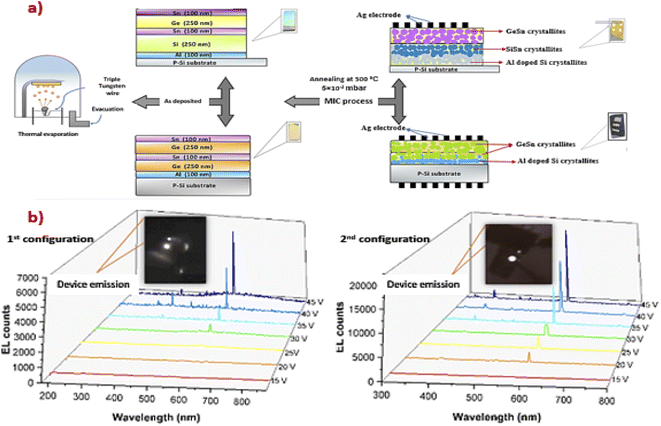
As we mentioned, random lasing does not require a cavity to resonate the photons inside for stimulated emission but the scattered photons between the material particles are involved in stimulating the electrons in the upper level to decay, and stimulated emission occurs. Thus, a heterostructure is prepared using photolithography for cavity fabrication. M. A. Nawwar et al. prepared multilayers of Al/Si/Sn/Ge/Sn and Al/Ge/Sn/Ge/Sn on the FTO substrate. These multilayers were then heat treated at 500 °C at a low vacuum level so that the MIC process formed Ge-doped Sn nanocrystallites; then, Ag electrodes were deposited as a front contact for electrical pumping, as shown in Fig. 42a. They studied the random lasing characteristics of the prepared GeSn heterostructures via the electroluminescence technique at different biasing voltages. They found that at a low voltage of biasing, the sample emitted spontaneously. By increasing the biasing voltage in the range of 15–45 V, random lasing spikes appeared at different regions of the spectra in UV, visible, and NIR due to oxygen incorporation in the GeSn network with the aid of low vacuum and a main lasing line at 590 nm with very small FWHM equal to 2.168 nm, as shown in Fig. 42b.16
 |
| | Fig. 42 Random lasing in GeSn nanocrystallites based on Al/Si/Sn/Ge/Sn and Al/Ge/Sn/Ge/Sn configurations. “Reproduced from ref. 11 https://www.researchsquare.com/article/rs-1406504/latest.pdf CC BY 4.0”. | |
1.6. Controlling the spectral responsivity, cut-off wavelength, and dark current for GeSn photodetectors (PDs)
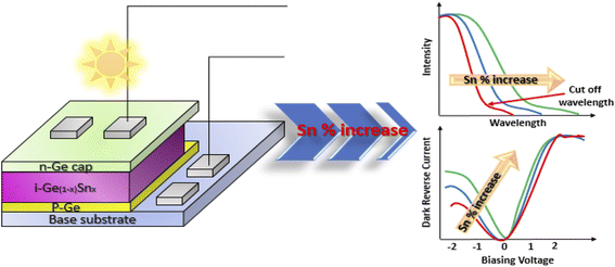
Sn incorporation in Ge networks increases the absorption coefficient of the GeSn compound. It is due to the shrinkage of the GeSn bandgap relative to Ge; thus, the responsivity increases. On the other hand, the dark current increases as the Sn content increases, as illustrated in Fig. 43.154,155 Sn incorporation causes the shrinking of the optical bandgap of the GeSn compound. This is due to the shallow levels in which the populated charge carriers can be easily thermally activated, causing thermally-induced reverse dark current.156,157 In this section, we will investigate how researchers increase the Sn content by increasing the Sn incorporation by many means as well as their impact on the photodetection process. Fig. 43 shows the schematic diagram of p–i–n GeSn-based heterostructure that serves as a photodetector device consists of the intrinsic layer of GeSn sandwiched between the p-Ge buffer layer and the n-Ge cap layer. With the increase in the Sn content, the responsivity and cut-off wavelength increase, but the dark reverse current worthy increases, as shown in the right-hand side of Fig. 43.
 |
| | Fig. 43 Impact of Sn content on spectral responsivity, cut-off wavelength, and dark current for GeSn PDs. | |
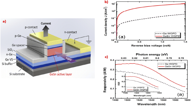
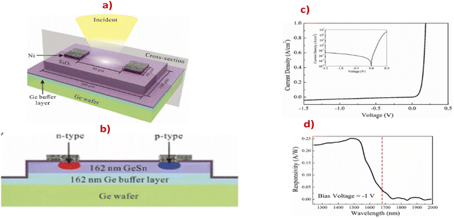
Yu-Hsiang Peng et al. compared the p–i–n GeSn photodetector with the Ge reference detector. They grew Ge/GeSn/Ge heterostructures of thicknesses 15/300/15 nm on the n-Ge on Ge/Si virtual substrate, respectively, and then capped p-Ge, as shown in Fig. 44a. SiO2 covered the prepared structure for passivation, followed by Ni electrodes. The Sn content was 1.78%. The prepared GeSn-based heterostructure gave 6.74 A cm−2, while the analogous Ge-based heterostructure gave 0.184 A cm−2, as shown in Fig. 44b. The responsivity of GeSn was 0.270 A W−1 and decayed smoothly compared to the Ge responsivity, which was equal to 0.189 A W−1 with rapid decay for incident light at 1550 nm, as shown in Fig. 44c.158
 |
| | Fig. 44 Comparison between the p–i–n GeSn photodetector and Ge reference detector responsivities and dark currents. “Reproduced from ref. 158 with permission from [American Institute of Physics publisher], copyright [2014]”. | |
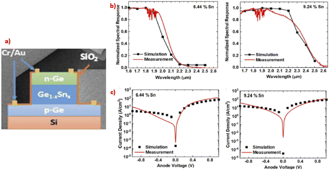
Hao Zhou et al. attempted to enhance the GeSn-based PD responsivity using plasmonic surface resonance. At first, they deposited a 964 nm of 8% Sn containing GeSn layer on the Ge/Si virtual substrate. The top 500 nm of the GeSn layer was of high quality with low dislocations. The Au array-like grating was fabricated on the surface of the GeSn layer by two step E-lithography for optical confinement via light scattering from the Au grating light array inside the GeSn structure. They obtained high responsivity for TM-polarized illumination of value 0.445 A W−1 at 1.5 V.159 Many studies have investigated the impact of Sn content increase on GeSn photodetectors (PDs) performance. Huong Tran et al. showed higher responsivity, higher dark current, and redshift of the cut-off wavelength for higher concentrations of Sn. They grew GeSn intrinsic layer sandwiched between p-Ge as a buffer and n-Ge as a capping layer, as seen in Fig. 45a, and then they prepared two samples of this set with Sn concentrations of 6.44% and 9.24%. They obtained responsivity values of 0.12 and 0.19 A W−1 and cut-off at 2.2 and 2.5 μm for 6.44 and 9.24% Sn content, respectively, as shown in Fig. 45b. The reverse current of 9.24% Sn concentration was higher than 6.44% (see Fig. 45c).160
 |
| | Fig. 45 Spectral responsivity and the reverse current for p-Ge/GeSn/n-Ge heterostructures with 6.44 and 9.24% Sn content. “Reproduced from ref. 160 https://www.frontiersin.org/articles/10.3389/fmats.2019.00278/full CC BY 4.0”. | |
As Sn incorporation in the Ge network causes more dislocation in the GeSn lattice that increases the dark current, the relaxed GeSn structure is desired in low dark current PD manufacturing. Yuekun Yang et al. tried to fabricate a relaxed bent dual GeSn/Ge nanowire. The bending of nanowires will relax the compressively strained GeSn with ≃10% Sn content. This promising structure reduced the dark current to very low values in the pA cm−2 range with responsivity of 1.2 mA W−1 with cut-off wavelength at 2200 nm.161 Liming Wang et al. tried to relax the GeSn strained network with the aid of the growth temperature and the annealing process under vacuum to release dislocation to reduce the dark current and hence enhance the spectral responsivity. They deposited 200 nm of Ge at 300 °C, followed by 300 nm of another Ge at 450 °C and by the GeSn layer with graded Sn content from 3% to 10%. After that, they annealed these layers in temperature ranging between 350 and 750 °C, which is the segregation temperature of Sn. Then, they obtained ridge waveguide p–i–n PD. The dark current dropped from 0.45 to 0.2 μA at −0.5 V, and the spectral responsivity was enhanced by 33% for the annealed PD compared to the as-deposited one.162 Huong Tran et al. demonstrated the enhancement of responsivity and detection limit of GeSn-based photodetector up to the mid-IR range with increasing Sn content from 10.5% to 22.3%.163 They prepared p-Ge on the Si substrate by controlling the flow of SnCl4; they obtained p-GeSn multilayers of the step increase of the Sn content, followed by the passivation layer (Fig. 46a). They used the interdigitated electrode technology to reduce the time of carrier recombination to decrease the dark reverse current during reverse biasing, as shown in Fig. 46b. The following table summarizes the concentrations of the samples with their responsivity values and the cut-off edge.
 |
| | Fig. 46 GeSn-based photodetector devices on Si substrate (a), effect of applied voltage on the current densities (b), and cut-off wavelength edge (c) cut-off wavelength with respect to different temperatures. “Reproduced from ref. 163 with permission from [American Chemical Society publisher], copyright [2019]”. | |
It is seen that the responsivity increased up to 3.2 × 10⁻³ A cm−2 and the cut-off wavelength edge increased up to 3.65 mm in the range of mid-infrared spectra with the increase in the Sn concentration to 22.3% from Table 6. Fig. 46c shows the increase in the cut-off edge and smooth responsivity decay with increasing Sn content from 10.5 to 22.3%.163
Table 6 Effect of Sn concentration on the responsivity and cut-off wavelength of GeSn photodetectors.163
| Sample158 |
Max. Sn% |
Responsivity (A W−1) |
Cut off wavelength (μm) |
| A |
12.5% |
2.0 |
2.95 |
| B |
15.9% |
4.4 × 10⁻² |
3.20 |
| C |
15.7% |
7.2 × 10⁻³ |
3.40 |
| D |
17.9% |
3.8 × 10⁻³ |
3.35 |
| E |
20.0% |
6.7 × 10⁻³ |
3.65 |
| F |
22.3% |
3.2 × 10⁻³ |
3.65 |
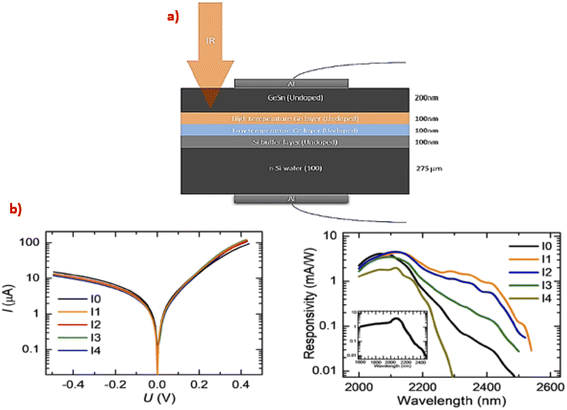
There are some works that aimed to increase the cut-off wavelength edge by inducing Sn incorporation and MQWs configurations. Patrik Cajev et al. attempted to induce Sn incorporation in the i-GeSn layer deposited on i-Ge virtual substrate consisting of 100 nm Ge deposited at low temperature (LT) and 100 nm of Ge deposited at high temperature (HT) on an Si-based substrate, as shown in Fig. 47a. They investigated that at low annealing laser intensities, Sn was incorporated, causing shrinkage of the bandgap. On the other hand, at high intensities of laser annealing, Sn accumulated on the surface reduced the Sn content in GeSn and the bandgap became wider. Fig. 47b shows the increase in the cut-off wavelength and responsivity of the samples annealed at low intensities, which decreased at high intensities of laser annealing, while the change in the dark current is not significant.164
 |
| | Fig. 47 GeSn-based photodetector devices on Si substrate by Sn incorporation and MQWs configurations (a), effect of applied voltage on the current densities and cut-off wavelength edge (b). “Reproduced from ref. 164 with permission from [Elsevier Ltd], copyright [2021]”. | |
A. Gassenq et al. investigated the effect of multi quantum wells number on the responsivity and the cut-off wavelength of GeSn photodetector devices for short-wave infrared applications.165 They deposited different samples of different quantum wells sandwiched between Ge cap and the buffer layer on Si base substrate (Fig. 48a). They implied that the increase in the quantum wells number of GeSn causes the continuity of the transitions through different thicknesses of GeSn quantum wells. As the number of wells increases, the absorption coefficient increases and the responsivity increases. It causes a shrinking of the bandgap and, hence, the cut-off wavelengths are redshifted, as shown in Fig. 48b.
 |
| | Fig. 48 Processed GeSn photoconductive detector for surface illumination (a) and responsivity as a function of wavelength at 5 V bias for structures with 0, 1, 2, or 3 Ge0.91Sn0.09 quantum wells embedded in Ge (b). “Reproduced from ref. 165 https://opg.optica.org/oe/fulltext.cfm?uri=oe-20-25-27297%26id=246204 CC BY 4.0”. | |
There have been some reports for dark current reduction by decreasing the area of the capping layer down to the electrode. Xiuli Li et al. used mesa structure via inductive plasma etching to reduce p-GeSn/i-GeSn/i-Ge (PL)/n-Si heterostructure area, as shown in Fig. 49a. They found that the reduction of the mesa structure area decreases the dark current, as illustrated in Fig. 49b.166 A low dark current density of 112 mA cm−2 was achieved at a bias voltage of −1 V. At bias voltages of −1 V, the optical responsivity of the photodetector was 14 mA W−1 at 2 μm. In addition, this GeSn photodetector achieved a 3 dB bandwidth as high as 30 GHz, which is among the highest values for 2 μm wavelength optical communications. The excellent high-speed performance of this device proves that Si-based GeSn photodetectors have great potential in the new 2 μm communication band, which can effectively increase the communication capacity in the future.
 |
| | Fig. 49 (a) Structure of p-GeSn/i-GeSn/i-Ge (PL)/n-Si heterostructure devices and (b) effect of the applied voltage on the current densities. “Reproduced from ref. 166 https://opg.optica.org/prj/fulltext.cfm?uri=prj-9-4-494%26id=449450 CC BY 4.0”. | |
M. Atalla et al. made a heterostructure consisted of GeSn with graded Sn content from 1 to 9% buffer layer on the Ge virtual substrate, followed by 3 p–i–n layers with Sn content of 8, 10, and 11.5%, respectively. Then, these multilayers were etched to form circular bumps shaped like PD. They obtained responsivity of 0.3 A W−1 with a cut-off wavelength equal to 2600 nm.167 Kuo-Chih Lee et al. used the planar configuration of electrodes rather than the perpendicular to reduce the area of the active layer under the electrode to overcome the recombination of the charge carriers with the electrodes.168 They deposited i-GeSn on the virtual Ge/Si substrate. p and n-GeSn spots are deposited on the intrinsic layer covered by the electrodes, as seen in Fig. 50a and b. They obtained low dark current via the planar configuration of the electrodes, as shown in Fig. 50c. In this work, a low dark current density was demonstrated, which corresponds to a high specific detectivity compared to the vertical GeSn photodiode (Fig. 50d). They present a foundry-compatible photodetector with high detectivity, thus facilitating potential practical applicability.
 |
| | Fig. 50 (a) Structure of GeSn/i-GeSn on Ge wafer devices, (b) cross section of the device, (c) effect of applied voltage on the current density, and (d) responsivity of the diode at a bias voltage of −1 V. “Reproduced from ref. 168 with permission from [American Institute of Physics publisher], copyright [2020]”. | |
1.7. GeSn-based metal oxide semiconductor field effect transistor (MOSFET) and GeSn FinFETs
MOSFETs are composed of n-type semiconductors; one is called the source and the other is called the drain separated by the gate of metal oxide of a defined length. The source, drain, and gate are mounted on the substrate as the base to work as an On/Off switch gate, as shown in Fig. 51.169
 |
| | Fig. 51 Schematic diagram of MOSFET transistor construction. “Reproduced from ref. 169 https://nanoscalereslett.springeropen.com/articles/10.1186/1556-276X-7-467 CC BY 2.0”. | |
A high quality transistor is featured by low subthreshold swing and higher drain current to give higher mobility of electrons between the source and drain, resulting in the lower switching gate voltage. Many works have attempted to enhance the featured parameters of MOSFETs based on GeSn that will be discussed in this section. Jiuren Zhou et al. fabricated pFET as follows: GeSn with a thickness equal to 6.8 nm with 4% Sn content as a quantum well channel was grown on the n-Ge (001) substrate. The p-type dopant was implemented to prepare the p-source and the drain. After that, the passivation process was run by flowing Si2H6, then the TaN/HZO/TaN/HfO2 stack was deposited as a gate (see Fig. 52a). They achieved sub-20 mV per decade subthreshold swing (Fig. 52b) and the mobility was enhanced.170
 |
| | Fig. 52 (a) Schematic diagram of the TaN/HZO/TaN/HfO2 stack gate GeSn-based transistor, (b) subthreshold swing versus drain current of the prepared transistor at different biasing voltage. “Reproduced from ref. 170 with permission from [IEEE publisher], copyright [2017]”. | |
The same group of Genquan Han et al. reported a study to enhance the mobility of the carriers between the source and the drain via the fabrication of the MOSFETs on different oriented base substrates. They fabricated the same configuration on different oriented Si substrate (001) and (111). The p-type MOSFET fabricated on Si (111) achieved 31% of ION at VDS = −1 V higher than that on Si (001). This is because the Si (111) base serves in the growth of more perfect crystalline GeSn quantum well channel.171 They studied the effect of the base orientation. They fabricated their configuration on (100)- and (111)-oriented Ge0.958Sn0.042 bases. The fabricated p-GeSn FET on (111) GeSn obtains higher mobility with an increase of 18% than the devices on the (100) GeSn substrate. This is because the (111) GeSn base has relaxed compressive strain that releases GeSn dislocations and hence enhance the carrier mobility compared to the (100) GeSn base.172 This group has another trial to relax the compressive strain in GeSn with the aid of GeSn fin structure. The line-constructed fins shown in figure were fabricated on (001)-oriented GeSn buffer on the SiO2 insulating layer. These tensile strained fins were grown in different orientations. ION obtained from (110)-oriented Ge0.90Sn0.10 line-Fin TFETs improved by 96.7% compared to the (100)-oriented Ge0.90Sn0.10 line-Fin TFETs.173 Ruben R. Lieten et al. employed the annealing process after growth to get +0.32% tensile-strained GeSn-based MOSFET. They grew 10 nm of amorphous GeSn channel layer on Si (111). This amorphous layer is then annealed to form tensile strained (111)-oriented single crystalline GeSn. NiGeSn drain and source were fabricated. Then, the stack of TaN/Al2O3 as a gate was deposited. The very thin 10 nm GeSn channel reaches the on/off ratio up to 84.174
2. Conclusions and outlook
In this review, different methodologies of controlling the strain engineering in the GeSn compound for bandgap modulation are deeply reviewed either by Sn incorporation that changes the Ge lattice parameters, heavy doping, nanomembrane design, or by external stress generation methods that results in stress GeSn stressor interface. Throughout the review, we illustrated how the emission of the GeSn compound intensity broadened and the peak position changed by structural modulation, different configured heterostructures, or external applied fields, and how to reduce the emission from the indirect transition. We also illustrated the GeSn MDs fabrication for LED, lasing, and photodetector devices. Also, reviewing and discussing the state-of-the-art of GeSn emission for LED applications and how to control the emission position, intensity, and broadening were carried out. Illustrating the fabrication of GeSn microcavities for lasing applications and how to control the intensity and position of lasing lines are examined, and threshold pumping required for pumping in different GeSn laser designations. How Sn incorporation controls the responsivity intensity and detection wavelength cut-off and how to overcome the dark leakage current for photodetection applications in NIR and mid-IR region for telecommunication applications have been discussed. The following have been highlighted: (1) random laser mechanism that occurs due to light photon scattering between the active media particles results in the emission of incoherent out of phase beam to form lasing spikes at different regions; (2) the regular lasing mechanism that requires an optical cavity composed of two reflective mirrors to guide the spontaneously emitted photons that are reflected back to the active media, stimulating the electrons to the upper lasing level to decay and become coherent in phase emission in the form of an intense sharp lasing line. We also illustrated the enhancement of the mobility within the gate of the GeSn-based transistor either by different oriented bases that relax the compressive strain and remove the dislocations that drop the carrier mobility, or annealing after GeSn growth or with the aid of relaxed GeSn fins-based transistor.
By these means, researchers in the above field can overcome compressive strain by developing novel structures such as NMs with higher flexibility, for example, natural bacterial cellulose membranes that contain voids and can help in GeSn relaxation. They can also enhance and control indirect-to-direct emission by many reviewed methods for bandgap manipulation of these compounds for LED applications in the mid-IR-NIR spectral region and for lasing applications with a very narrow lasing mode. The solubility of Pb in Ge can tune the bandgap of mid and far infrared direct emission for telecommunication applications rather than the low solubility of Sn. The Pb content will be the key for tuning and controlling the bandgap with few percentages rather than Sn. It will also help in raising the operating temperature near the room temperature and the reduction of the pumping power threshold. In addition, it will serve in developing physical devices such as semiconducting sensors and optical signal waveguiding for IoT networks.
Conflicts of interest
There are no conflicts to declare.
References
- S. Kumar, P. Tiwari and M. Zymbler, Internet of Things is a revolutionary approach for future technology enhancement: a review, J. Big Data, 2019, 6(1), 1–21 CrossRef CAS.
- D. Liang and J. E. Bowers, Recent progress in lasers on silicon, Nat. Photonics, 2010, 4(8), 511–517 CrossRef CAS.
- A. Ghazala, Composition and electronic properties of a-SiGe: H alloys produced from ultrathin layers of a-Si: H/a-Ge: H, J. Mater. Sci.: Mater. Electron., 2000, 11(5), 429–432 CrossRef.
- M. A. Ghazala, W. Beyer and H. Wagner, Long-term stability of hydrogenated amorphous germanium measured by infrared absorption, J. Appl. Phys., 1991, 70(8), 4540–4543 CrossRef CAS.
- Y. Zhu, X. Wang and W. Mi, Strain and electric field modulated electronic structure of two-dimensional SiP (SiAs)/GeS van der Waals heterostructures, J. Mater. Chem. C, 2019, 7(34), 10491–10497 RSC.
- V. Alex, S. Finkbeiner and J. Weber, Temperature dependence of the indirect energy gap in crystalline silicon, J. Appl. Phys., 1996, 79(9), 6943–6946 CrossRef CAS.
- S. Wirths, D. Buca and S. Mantl, Si–Ge–Sn alloys: From growth to applications, Prog. Cryst. Growth Charact. Mater., 2016, 62(1), 1–39 CrossRef CAS.
- C. Si, J. Liu, Y. Xu, J. Wu, B. L. Gu and W. Duan, Functionalized germanene as a prototype of large-gap two-dimensional topological insulators, Phys. Rev. B, 2014, 89(11), 115429 CrossRef.
- N. von den Driesch, D. Stange, S. Wirths, D. Rainko, I. Povstugar, A. Savenko and D. Buca, SiGeSn ternaries for efficient group IV heterostructure light emitters, Small, 2017, 13(16), 1603321 CrossRef PubMed.
- J. Menendez, P. M. Wallace, C. Xu, C. L. Senaratne, J. D. Gallagher and J. Kouvetakis, Materials physics of GeSn-based semiconductor lasers, Mater. Today: Proc., 2019, 14, 38–42 CAS.
- W. Du and S. Q. Yu. Group IV photonics using (Si) GeSn technology toward mid-IR applications. in Mid-infrared Optoelectronics, Woodhead Publishing, 2020, pp. 493–538 Search PubMed.
- R. Geiger, T. Zabel and H. Sigg, Group IV direct band gap photonics: methods, challenges, and opportunities, Front. Mater., 2015, 2, 52 Search PubMed.
- Y. Miao, G. Wang, Z. Kong, B. Xu, X. Zhao, X. Luo and H. H. Radamson, Review of Si-based GeSn CVD growth and optoelectronic applications, Nanomaterials, 2021, 11(10), 2556 CrossRef CAS PubMed.
- D. J. Lockwood and L. Pavesi, Silicon Photonics IV, Springer International Publishing, 2021, vol. 139 Search PubMed.
- M. S. Abo Ghazala, H. A. Othman, L. M. Sharaf El-Deen, M. A. Nawwar and A. E. H. B. Kashyout, Fabrication of Nanocrystalline Silicon Thin Films Utilized for Optoelectronic Devices Prepared by Thermal Vacuum Evaporation, ACS Omega, 2020, 5(42), 27633–27644 CrossRef CAS PubMed.
- M. A. Nawwar, M. S. A. Ghazala, L. M. S. El-Deen, A. El-Shaer, B. Anis and A. E. H. B. Kashyout, Towards white light laser emission based on strained Poly:(Si/Ge), Research Square, 2022 Search PubMed.
- J. Andrade-Arvizu, R. Fonoll-Rubio, Y. Sánchez, I. Becerril-Romero, C. Malerba, M. Valentini and Z. Jehl Li-Kao, Rear Band gap Grading Strategies on Sn–Ge-Alloyed Kesterite Solar Cells, ACS Appl. Energy Mater., 2020, 3(11), 10362–10375 CrossRef CAS.
- K. W. J. Barnham and G. Duggan, A new approach to high-efficiency multi-bandgap solar cells, J. Appl. Phys., 1990, 67(7), 3490–3493 CrossRef CAS.
- J. Vuckovic and K. Saraswat. Silicon Compatible Electrically Pumped Direct Bandgap Ge/GeSn Laser. Leland Stanford Junior University Stanford, United States, 2019 Search PubMed.
- A. Chaves, J. G. Azadani, H. Alsalman, D. R. Da Costa, R. Frisenda, A. J. Chaves and T. Low, Bandgap engineering of two-dimensional semiconductor materials, npj 2D Mater. Appl., 2020, 4(1), 1–21 CrossRef.
- S. Deng, A. V. Sumant and V. Berry, Strain engineering in two-dimensional nanomaterials beyond graphene, Nano Today, 2018, 22, 14–35 CrossRef CAS.
- L. Wang, Z. Zhang and X. Han, In situ experimental mechanics of nanomaterials at the atomic scale, NPG Asia Mater., 2013, 5(2), e40 CrossRef CAS.
- Y. Kang, Y. C. Huang, K. H. Lee, S. Bao, W. Wang, D. Lei and Y. C. Yeo, Strain relaxation of germanium-tin (GeSn) fins, AIP Adv., 2018, 8(2), 025111 CrossRef.
- A. R. Denton and N. W. Ashcroft, Vegard's law, Phys. Rev. A, 1991, 43(6), 3161 CrossRef CAS PubMed.
- S. Xu, Y. C. Huang, K. H. Lee, W. Wang, Y. Dong, D. Lei and Y. C. Yeo, GeSn lateral pin photodetector on insulating substrate, Opt. Express, 2018, 26(13), 17312–17321 CrossRef CAS PubMed.
- P. C. Eng, S. Song and B. Ping, State-of-the-art photodetectors for optoelectronic integration at telecommunication wavelength, Nanophotonics, 2015, 4(3), 277–302 CAS.
- M. El Kurdi, G. Fishman, S. Sauvage and P. Boucaud, Band structure and optical gain of tensile-strained germanium based on a 30 band k·p formalism, J. Appl. Phys., 2010, 107(1), 013710 CrossRef.
- J. Mathews, R. T. Beeler, J. Tolle, C. Xu, R. Roucka, J. Kouvetakis and J. Menendez, Direct-gap photoluminescence with tunable emission wavelength in Ge 1− y Sn y alloys on silicon, Appl. Phys. Lett., 2010, 97(22), 221912 CrossRef.
- J. R. Jain, A. Hryciw, T. M. Baer, D. A. Miller, M. L. Brongersma and R. T. Howe, A micromachining-based technology for enhancing germanium light emission via tensile strain, Nat. Photonics, 2012, 6(6), 398–405 CrossRef CAS.
- S. Assali, M. Albani, R. Bergamaschini, M. A. Verheijen, A. Li, S. Kölling and L. Miglio, Strain engineering in Ge/GeSn core/shell nanowires, Appl. Phys. Lett., 2019, 115(11), 113102 CrossRef.
- M. Albani, S. Assali, M. A. Verheijen, S. Koelling, R. Bergamaschini, F. Pezzoli and L. Miglio, Critical strain for Sn incorporation into spontaneously graded Ge/GeSn core/shell nanowires, Nanoscale, 2018, 10(15), 7250–7256 RSC.
- J. Chrétien, N. Pauc, F. Armand Pilon, M. Bertrand, Q. M. Thai, L. Casiez and V. Calvo, GeSn lasers covering a wide wavelength range thanks to uniaxial tensile strain, ACS Photonics, 2019, 6(10), 2462–2469 CrossRef.
- S. Gupta, R. Chen, Y. C. Huang, Y. Kim, E. Sanchez, J. S. Harris and K. C. Saraswat, Highly Selective Dry Etching of Germanium over Germanium–Tin (Ge1−xSnx): A Novel Route for Ge1−xSnx Nanostructure Fabrication, Nano Lett., 2013, 13(8), 3783–3790 CrossRef CAS.
- S. Wirths, D. Stange, M. A. Pampillón, A. T. Tiedemann, G. Mussler, A. Fox and D. Buca, High-k gate stacks on low bandgap tensile strained Ge and GeSn alloys for field-effect transistors, ACS Appl. Mater. Interfaces, 2015, 7(1), 62–67 CrossRef CAS PubMed.
- Y. Han, Y. Song, X. Chen, Z. Zhang, J. Liu, Y. Li and S. Wang, Abnormal strain in suspended GeSn microstructures, Mater. Res. Express, 2018, 5(3), 035901 CrossRef.
- A. Elbaz, D. Buca, N. von den Driesch, K. Pantzas, G. Patriarche, N. Zerounian and M. El Kurdi, Ultra-low-threshold continuous-wave and pulsed lasing in tensile-strained GeSn alloys, Nat. Photonics, 2020, 14(6), 375–382 CrossRef CAS.
- S. V. Ketov, Y. H. Sun, S. Nachum, Z. Lu, A. Checchi, A. R. Beraldin and A. L. Greer, Rejuvenation of metallic glasses by non-affine thermal strain, Nature, 2015, 524(7564), 200–203 CrossRef CAS.
- S. Ghosh and J. Choi, Modeling and experimental verification of transient/residual stresses and microstructure formation in multi-layer laser aided DMD process, J. Heat Transfer, 2006, 128(7), 662–679 CrossRef CAS.
- H. Oka, T. Amamoto, M. Koyama, Y. Imai, S. Kimura, T. Hosoi and H. Watanabe, Fabrication of tensile-strained single-crystalline GeSn on transparent substrate by nucleation-controlled liquid-phase crystallization, Appl. Phys. Lett., 2017, 110(3), 032104 CrossRef.
- Y. C. Tai, P. L. Yeh, S. An, H. H. Cheng, M. Kim and G. E. Chang, Strain-free GeSn nanomembranes enabled by transfer-printing techniques for advanced optoelectronic applications, Nanotechnology, 2020, 31(44), 445301 CrossRef CAS PubMed.
- S. An, Y. C. Tai, K. C. Lee, S. H. Shin, H. H. Cheng, G. E. Chang and M. Kim, Raman scattering study of GeSn under< 1 0 0> and< 1 1 0> uniaxial stress, Nanotechnology, 2021, 32(35), 355704 CrossRef CAS PubMed.
- Q. Chen, S. Wu, L. Zhang, H. Zhou, W. Fan and C. S. Tan, Transferable single-layer GeSn nanomembrane resonant-cavity-enhanced photodetectors for 2 μm band optical communication and multi-spectral short-wave infrared sensing, Nanoscale, 2022, 14(19), 7341–7349 RSC.
- S. An, Y. Liao and M. Kim, Flexible Titanium Nitride/Germanium-Tin Photodetectors Based on Sub-Bandgap Absorption, ACS Appl. Mater. Interfaces, 2021, 13(51), 61396–61403 CrossRef CAS PubMed.
- S. Barth, M. S. Seifner and J. Bernardi, Microwave-assisted solution–liquid–solid growth of Ge 1− x Sn x nanowires with high tin content, Chem. Commun., 2015, 51(61), 12282–12285 RSC.
- O. Gurdal, P. Desjardins, J. R. A. Carlsson, N. Taylor, H. H. Radamson, J. E. Sundgren and J. E. Greene, Low-temperature growth and critical epitaxial thicknesses of fully strained metastable Ge1−xSnx (x ≲ 0.26) alloys on Ge (001) 2 × 1, J. Appl. Phys., 1998, 83(1), 162–170 CrossRef CAS.
- W. Dou, M. Benamara, A. Mosleh, J. Margetis, P. Grant, Y. Zhou and S. Q. Yu, Investigation of GeSn strain relaxation and spontaneous composition gradient for low-defect and high-Sn alloy growth, Sci. Rep., 2018, 8(1), 1–11 CAS.
- P. Onufrijevs, P. Ščajev, A. Medvids, M. Andrulevicius, S. Nargelas, T. Malinauskas and H. H. Cheng, Direct-indirect GeSn band structure formation by laser Radiation: The enhancement of Sn solubility in Ge, Opt. Laser Technol., 2020, 128, 106200 CrossRef CAS.
- E. Kasper, M. Kittler, M. Oehme and T. Arguirov, Germanium tin: silicon photonics toward the mid-infrared, Photonics Res., 2013, 1(2), 69–76 CrossRef.
- D. Stange, S. Wirths, N. von den Driesch, G. Mussler, T. Stoica, Z. Ikonic and D. Buca, Optical transitions in direct-bandgap Ge1−xSnx alloys, ACS Photonics, 2015, 2(11), 1539–1545 CrossRef CAS.
- B. Dutt, H. Lin, D. S. Sukhdeo, B. M. Vulovic, S. Gupta, D. Nam and J. S. Harris Jr, Theoretical analysis of GeSn alloys as a gain medium for a Si-compatible laser, IEEE J. Sel. Top. Quantum Electron., 2013, 19(5), 1502706 Search PubMed.
- T. D. Eales, I. P. Marko, S. Schulz, E. O'Halloran, S. Ghetmiri, W. Du and S. J. Sweeney, Ge1−xSnx alloys: consequences of band mixing effects for the evolution of the band gap Γ-character with Sn concentration, Sci. Rep., 2019, 9(1), 1–10 CrossRef CAS PubMed.
- A. Gassenq, L. Milord, J. Aubin, K. Guilloy, S. Tardif, N. Pauc and V. Calvo, Gamma bandgap determination in pseudomorphic GeSn layers grown on Ge with up to 15% Sn content, Appl. Phys. Lett., 2016, 109(24), 242107 CrossRef.
- M. Oehme, D. Buca, K. Kostecki, S. Wirths, B. Holländer, E. Kasper and J. Schulze, Epitaxial growth of highly compressively strained GeSn alloys up to 12.5% Sn, J. Cryst. Growth, 2013, 384, 71–76 CrossRef CAS.
- H. H. Huang, X. Fan, D. J. Singh and W. T. Zheng, The thermal and thermoelectric transport properties of SiSb, GeSb and SnSb monolayers, J. Mater. Chem. C, 2019, 7(34), 10652–10662 RSC.
- H. Alahmad, A. Mosleh, M. Alher, S. F. Banihashemian, S. A. Ghetmiri, S. Al-Kabi and H. A. Naseem, GePb alloy growth using layer inversion method, J. Electron. Mater., 2018, 47(7), 3733–3740 CrossRef CAS.
- W. Huang, B. Cheng, C. Xue and C. Li, Comparative studies of clustering effect, electronic and optical properties for GePb and GeSn alloys with low Pb and Sn concentration, Phys. B, 2014, 443, 43–48 CrossRef CAS.
- C. A. Broderick, E. J. O'Halloran and E. P. O'Reilly. First principles analysis of electronic structure evolution and the indirect-to direct-gap transition in Ge $ _ {1-x} $ Pb $ _ {x} $ group-IV alloys, arXiv, 2019, preprint arXiv:1911.05679.
- T. K. P. Luong, V. Le Thanh, A. Ghrib, M. El Kurdi and P. Boucaud, Enhanced Tensile Strain in P-doped Ge Films Grown by Molecular Beam Epitaxy Using GaP and Sb Solid Sources, J. Electron. Mater., 2019, 48(7), 4674–4678 CrossRef CAS.
- A. Rajabi-Maram, N. Hasani and S. B. Touski, Tuning electronic properties of MSb (M= C, Si, Ge and Sn) monolayers by strain engineering, Phys. E, 2022, 138, 115065 CrossRef CAS.
- S. Zaima, O. Nakatsuka, N. Taoka, M. Kurosawa, W. Takeuchi and M. Sakashita, Growth and applications of GeSn-related group-IV semiconductor materials, Sci. Technol. Adv. Mater., 2015, 16(4), 043502 CrossRef.
- H. Li, J. Brouillet, A. Salas, X. Wang and J. Liu, Low temperature growth of high crystallinity GeSn on amorphous layers for advanced optoelectronics, Opt. Mater. Express, 2013, 3(9), 1385–1396 CrossRef.
- H. Khelidj, A. Portavoce, M. Bertoglio, M. Descoins, L. Patout, K. Hoummada and D. Mangelinck, Ge (Sn) growth on Si (001) by magnetron sputtering, Mater. Today Commun., 2021, 26, 101915 CrossRef CAS.
- W. Dou, B. Alharthi, P. C. Grant, J. M. Grant, A. Mosleh, H. Tran and S. Q. Yu, Crystalline GeSn growth by plasma enhanced chemical vapor deposition, Opt. Mater. Express, 2018, 8(10), 3220–3229 CrossRef CAS.
- Z. P. Zhang, Y. X. Song, Z. Y. S. Zhu, Y. Han, Q. M. Chen, Y. Y. Li and S. M. Wang, Structural properties of GeSn thin films grown by molecular beam epitaxy, AIP Adv., 2017, 7(4), 045211 CrossRef.
- M. Schatzl, F. Hackl, M. Glaser, P. Rauter, M. Brehm, L. Spindlberger and F. Schäffler, Enhanced telecom emission from single group-IV quantum dots by precise CMOS-compatible positioning in photonic crystal cavities, ACS Photonics, 2017, 4(3), 665–673 CrossRef CAS PubMed.
- Q. Chen, L. Zhang, Y. Song, X. Chen, S. Koelling, Z. Zhang and Q. Gong, Highly tensile-strained self-assembled Ge quantum dots on InP substrates for integrated light sources, ACS Appl. Nano Mater., 2021, 4(1), 897–906 CrossRef CAS.
- B. Schwartz, T. Arguirov, M. Kittler, M. Oehme, K. Kostecki, E. Kasper and J. Schulze. Comparison of EL emitted by LEDs on Si substrates containing Ge and Ge/GeSn MQW as active layers. in Silicon Photonics X, SPIE, 2015, vol. 9367, pp. 298–305, February Search PubMed.
- J. Doherty, S. Biswas, E. Galluccio, C. A. Broderick, A. Garcia-Gil, R. Duffy and J. D. Holmes, Progress on germanium–tin nanoscale alloys, Chem. Mater., 2020, 32(11), 4383–4408 CrossRef CAS.
- R. Chen, H. Lin, Y. Huo, C. Hitzman, T. I. Kamins and J. S. Harris, Increased photoluminescence of strain-reduced, high-Sn composition Ge1−xSnx alloys grown by molecular beam epitaxy, Appl. Phys. Lett., 2011, 99(18), 181125 CrossRef.
- H. S. Mączko, R. Kudrawiec and M. Gladysiewicz, Material gain engineering in GeSn/Ge quantum wells integrated with an Si platform, Sci. Rep., 2016, 6(1), 1–11 CrossRef PubMed.
- T. Liu, Y. Miao, L. Wang, G. Zhu, H. Hu, Z. Zhong and Z. Jiang, Temperature dependence of Raman scattering in GeSn films, J. Raman Spectrosc., 2020, 51(7), 1092–1099 CrossRef CAS.
- B. Wang, M. R. Hogsed, T. R. Harris, P. M. Wallace and J. Kouvetakis, Enhanced optical and electrical performance of Ge1−xSnx/Ge/Si (100) (x = 0.062) semiconductor via inductively coupled H2 plasma treatments, Semicond. Sci. Technol., 2019, 34(4), 045014 CrossRef CAS.
- R. Chen, S. Gupta, Y. C. Huang, Y. Huo, C. W. Rudy, E. Sanchez and J. S. Harris, Demonstration of a Ge/GeSn/Ge quantum-well microdisk resonator on silicon: enabling high-quality Ge (Sn) materials for micro-and nanophotonics, Nano Lett., 2014, 14(1), 37–43 CrossRef CAS PubMed.
- S. A. Ghetmiri, W. Du, J. Margetis, A. Mosleh, L. Cousar, B. R. Conley and S. Q. Yu, Direct-bandgap GeSn grown on silicon with 2230 nm photoluminescence, Appl. Phys. Lett., 2014, 105(15), 151109 CrossRef.
- D. Rainko, Z. Ikonic, N. Vukmirović, D. Stange, N. von den Driesch, D. Grützmacher and D. Buca, Investigation of carrier confinement in direct bandgap GeSn/SiGeSn 2D and 0D heterostructures, Sci. Rep., 2018, 8(1), 1–13 CAS.
- G. Grzybowski, L. Jiang, J. Mathews, R. Roucka, C. Xu, R. T. Beeler and J. Menendez, Photoluminescence from heavily doped GeSn: P materials grown on Si (100), Appl. Phys. Lett., 2011, 99(17), 171910 CrossRef.
- Y. Miao, Y. Wang, H. Hu, X. Liu, H. Su, J. Zhang and H. Zhang, Characterization of crystalline GeSn layer on tensile-strained Ge buffer deposited by magnetron sputtering, Mater. Sci. Semicond. Process., 2018, 85, 134–140 CrossRef CAS.
- Z. Kong, G. Wang, R. Liang, J. Su, M. Xun, Y. Miao and H. H. Radamson, Growth and Strain Modulation of GeSn Alloys for Photonic and Electronic Applications, Nanomaterials, 2022, 12(6), 981 CrossRef CAS.
- M. Grydlik, F. Hackl, H. Groiss, M. Glaser, A. Halilovic, T. Fromherz and M. Brehm, Lasing from glassy Ge quantum dots in crystalline Si, ACS Photonics, 2016, 3(2), 298–303 CrossRef CAS PubMed.
- L. Peng, X. Li, J. Zheng, X. Liu, M. Li, Z. Liu and B. Cheng, Room-temperature direct-bandgap electroluminescence from type-I GeSn/SiGeSn multiple quantum wells for 2 μm LEDs, J. Lumin., 2020, 228, 117539 CrossRef CAS.
- G. Sun, R. A. Soref and H. H. Cheng, Design of a Si-based lattice-matched room-temperature GeSn/GeSiSn multi-quantum-well mid-infrared laser diode, Opt. Express, 2010, 18(19), 19957–19965 CrossRef CAS PubMed.
- G. E. Chang, W. Y. Hsieh, J. Z. Chen and H. H. Cheng, Quantum-confined photoluminescence from Ge1−xSnx/Ge superlattices on Ge-buffered Si (001) substrates, Opt. Lett., 2013, 38(18), 3485–3487 CrossRef CAS PubMed.
- P. C. Grant, J. Margetis, Y. Zhou, W. Dou, G. Abernathy, A. Kuchuk and S. Q. Yu, Direct bandgap type-I GeSn/GeSn quantum well on a GeSn-and Ge-buffered Si substrate, AIP Adv., 2018, 8(2), 025104 CrossRef.
- J. Yang, H. Hu, Y. Miao, L. Dong, B. Wang, W. Wang and H. Zhang, High-quality GeSn layer with Sn composition up to 7% grown by low-temperature magnetron sputtering for optoelectronic application, Materials, 2019, 12(17), 2662 CrossRef CAS.
- A. C. Meng, Y. Wang, M. R. Braun, J. Z. Lentz, S. Peng, H. Cheng and P. C. McIntyre, Bending and precipitate formation mechanisms in epitaxial Ge-core/GeSn-shell nanowires, Nanoscale, 2021, 13(41), 17547–17555 RSC.
- S. Assali, A. Dijkstra, A. Attiaoui, É. Bouthillier, J. E. Haverkort and O. Moutanabbir, Midinfrared Emission and Absorption in Strained and Relaxed Direct-Band-Gap Ge1−xSnx Semiconductors, Phys. Rev. Appl., 2021, 15(2), 024031 CrossRef CAS.
- D. Burt, H. J. Joo, Y. Jung, Y. Kim, M. Chen, Y. C. Huang and D. Nam, Strain-relaxed GeSn-on-insulator (GeSnOI) microdisks, Opt. Express, 2021, 29(18), 28959–28967 CrossRef CAS PubMed.
- C. Y. Lin, H. Y. Ye, F. L. Lu, H. S. Lan and C. W. Liu, Biaxial strain effects on photoluminescence of Ge/strained GeSn/Ge quantum well, Opt. Mater. Express, 2018, 8(9), 2795–2802 CrossRef CAS.
- S. Assali, J. Nicolas, S. Mukherjee, A. Dijkstra and O. Moutanabbir, Atomically uniform Sn-rich GeSn semiconductors with 3.0–3.5 μm room-temperature optical emission, Appl. Phys. Lett., 2018, 112(25), 251903 CrossRef.
- T. Liu, L. Wang, G. Zhu, X. Hu, Z. Dong, Z. Zhong and Z. Jiang, Dislocation-related photoluminescence of GeSn films grown on Ge (001) substrates by molecular beam epitaxy, Semicond. Sci. Technol., 2018, 33(12), 125022 CrossRef.
- R. R. Lieten, J. W. Seo, S. Decoster, A. Vantomme, S. Peters, K. C. Bustillo and J. P. Locquet, Tensile strained GeSn on Si by solid phase epitaxy, Appl. Phys. Lett., 2013, 102(5), 052106 CrossRef.
- R. R. Lieten, C. Fleischmann, S. Peters, N. M. Santos, L. M. Amorim, Y. Shimura and A. Vantomme, Structural and optical properties of amorphous and crystalline GeSn layers on Si, ECS J. Solid State Sci. Technol., 2014, 3(12), P403 CrossRef CAS.
- P. Zaumseil, Y. Hou, M. A. Schubert, N. Von Den Driesch, D. Stange, D. Rainko and G. Capellini, The thermal stability of epitaxial GeSn layers, APL Mater., 2018, 6(7), 076108 CrossRef.
- M. Wang, K. E. Lee, S. H. Hahn, E. J. Kim, S. Kim, J. S. Chung and C. Park, Optical and photoluminescent properties of sol-gel Al-doped ZnO thin films, Mater. Lett., 2007, 61(4–5), 1118–1121 CrossRef CAS.
- R. Röder, S. Geburt, M. Zapf, D. Franke, M. Lorke, T. Frauenheim and C. Ronning, Transition metal and rare earth element doped zinc oxide nanowires for optoelectronics, Phys. Status Solidi B, 2019, 256(4), 1800604 CrossRef.
- L. Zhang, H. Hong, K. Qian, S. Wu, G. Lin, J. Wang and C. Li, Controllable synthesis of Si-based GeSn quantum dots with room-temperature photoluminescence, Appl. Surf. Sci., 2022, 579, 152249 CrossRef CAS.
- L. Peng, X. Li, Z. Liu, X. Liu, J. Zheng, C. Xue and B. Cheng, Horizontal GeSn/Ge multi-quantum-well ridge waveguide LEDs on silicon substrates, Photonics Res., 2020, 8(6), 899–903 CrossRef CAS.
- H. Li, C. Chang, T. P. Chen, H. H. Cheng, Z. W. Shi and H. Chen, Characteristics of Sn segregation in Ge/GeSn heterostructures, Appl. Phys. Lett., 2014, 105(15), 151906 CrossRef.
- Y. S. Huang, Y. J. Tsou, C. H. Huang, C. H. Huang, H. S. Lan, C. W. Liu and S. Kuppurao, High-mobility CVD-grown Ge/strained Ge 0.9 Sn 0.1/Ge quantum-well pMOSFETs on Si by optimizing Ge cap thickness, IEEE Trans. Electron Devices, 2017, 64(6), 2498–2504 CAS.
- S. Yang, B. H. Lin, W. R. Liu, J. H. Lin, C. S. Chang, C. H. Hsu and W. F. Hsieh, Structural characteristics and annealing effect of ZnO epitaxial films grown by atomic layer deposition, Cryst. Growth Des., 2009, 9(12), 5184–5189 CrossRef CAS.
- D. Wang, X. Gao, J. Tang, X. Fang, D. Fang, X. Wang and Z. Wei, Emission characteristics variation of GaAs0. 92Sb0. 08/Al0. 3Ga0. 7As strained multiple quantum wells caused by rapid thermal annealing, Sci. Rep., 2021, 11(1), 1–7 CrossRef.
- S. Ghosh, K. C. Lin, C. H. Tsai, H. Kumar, Q. Chen, L. Zhang and G. E. Chang, Metal-semiconductor-metal GeSn photodetectors on silicon for short-wave infrared applications, Micromachines, 2020, 11(9), 795 CrossRef PubMed.
- S. Ghosh, B. Mukhopadhyay and G. E. Chang, Design and analysis of GeSn-based resonant-cavity-enhanced photodetectors for optical communication applications, IEEE Sens. J., 2020, 20(14), 7801–7809 CAS.
- N. Yahyaoui, N. Sfina, J. L. Lazzari, A. Bournel and M. Said, Wave-function engineering and absorption spectra in Si0. 16Ge0. 84/Ge0. 94Sn0. 06/Si0. 16Ge0. 84 strained on relaxed Si0. 10Ge0. 90 type I quantum well, J. Appl. Phys., 2014, 115(3), 033109 CrossRef.
- S. Ghosh, H. Kumar, B. Mukhopadhyay and G. E. Chang, Design and Modeling of High-Performance DBR-Based Resonant-Cavity-Enhanced GeSn Photodetector for Fiber-Optic Telecommunication Networks, IEEE Sens. J., 2021, 21(8), 9900–9908 CAS.
- D. Rainko, Z. Ikonic, A. Elbaz, N. von den Driesch, D. Stange, E. Herth and D. Buca, Impact of tensile strain on low Sn content GeSn lasing, Sci. Rep., 2019, 9(1), 1–9 CrossRef CAS.
- J. Yang, H. Hu, Y. Miao, L. Dong, B. Wang, W. Wang and H. Zhang, High-quality GeSn layer with Sn composition up to 7% grown by low-temperature magnetron sputtering for optoelectronic application, Materials, 2019, 12(17), 2662 CrossRef CAS PubMed.
- Y. Zhou, W. Dou, W. Du, T. Pham, S. A. Ghetmiri, S. Al-Kabi and S. Q. Yu, Systematic study of GeSn heterostructure-based light-emitting diodes towards mid-infrared applications, J. Appl. Phys., 2016, 120(2), 023102 CrossRef.
- W. Du, Y. Zhou, S. A. Ghetmiri, A. Mosleh, B. R. Conley, A. Nazzal and S. Q. Yu, Room-temperature electroluminescence from Ge/Ge1-xSnx/Ge diodes on Si substrates, Appl. Phys. Lett., 2014, 104(24), 241110 CrossRef.
- D. Stange, N. Von Den Driesch, D. Rainko, C. Schulte-Braucks, S. Wirths, G. Mussler and D. Buca, Study of GeSn based heterostructures: towards optimized group IV MQW LEDs, Opt. Express, 2016, 24(2), 1358–1367 CrossRef CAS PubMed.
- D. Stange, N. von den Driesch, D. Rainko, S. Roesgaard, I. Povstugar, J. M. Hartmann and D. Buca, Short-wave infrared LEDs from GeSn/SiGeSn multiple quantum wells, Optica, 2017, 4(2), 185–188 CrossRef CAS.
- H. Cao, Lasing in random media, Waves Random Media, 2003, 13(3), R1 CrossRef.
- R. Scheps, Upconversion laser processes, Prog. Quantum Electron., 1996, 20(4), 271–358 CrossRef CAS.
- H. I. Lin, K. C. Shen, Y. M. Liao, Y. H. Li, P. Perumal, G. Haider and Y. F. Chen, Integration of nanoscale light emitters and hyperbolic metamaterials: an efficient platform for the enhancement of random laser action, ACS Photonics, 2017, 5(3), 718–727 CrossRef.
- A. S. Gomes, A. L. Moura, C. B. de Araújo and E. P. Raposo, Recent advances and applications of random lasers and random fiber lasers, Prog. Quantum Electron., 2021, 78, 100343 CrossRef.
- P. Srisamran, Nanosecond-Pumped Resonance Raman Random lasing from Micro-/Nano-granular Materials toward Chemical Detection from Distance, (Doctoral dissertation, Prince of Songkla University), 2019 Search PubMed.
- R. Sapienza, Determining random lasing action, Nat. Rev. Phys., 2019, 1(11), 690–695 CrossRef.
- R. G. El-Dardiry, A. P. Mosk, O. L. Muskens and A. Lagendijk, Experimental studies on the mode structure of random lasers, Phys. Rev. A, 2010, 81(4), 043830 CrossRef.
- D. S. Wiersma, The physics and applications of random lasers, Nat. Phys., 2008, 4(5), 359–367 Search PubMed.
- G. H. M. Van Tartwijk and D. Lenstra, Semiconductor lasers with optical injection and feedback, Quantum Semiclassical Opt., 1995, 7(2), 87 Search PubMed.
- H. Cao, R. Chriki, S. Bittner, A. A. Friesem and N. Davidson, Complex lasers with controllable coherence, Nat. Rev. Phys., 2019, 1(2), 156–168 Search PubMed.
- H. M. Gibbs, G. Khitrova and S. W. Koch, Exciton–polariton light–semiconductor coupling effects, Nat. Photonics, 2011, 5(5), 273 CrossRef.
- J. Kasprzak, M. Richard, S. Kundermann, A. Baas, P. Jeambrun, J. M. J. Keeling and L. S. Dang, Bose–Einstein condensation of exciton polaritons, Nature, 2006, 443(7110), 409–414 CrossRef CAS PubMed.
- S. Roling, B. Siemer, M. Wöstmann, H. Zacharias, R. Mitzner, A. Singer and I. A. Vartanyants, Temporal and spatial coherence properties of free-electron-laser pulses in the extreme ultraviolet regime, Phys. Rev. Spec. Top.--Accel. Beams, 2011, 14(8), 080701 CrossRef.
- S. Xu, Y. C. Huang, K. H. Lee, K. Han, D. Lei, W. Wang, Y. C. Yeo, Formation of GeSn Multiple-Quantum-Well Microdisks on Insulating Platform toward Lasing Applications, in CLEO: Science and Innovations, 2019, Optical Society of America, p. STu4J Search PubMed.
- R. Chen, S. Gupta, Y. C. Huang, Y. Huo, C. W. Rudy, E. Sanchez and J. S. Harris, Demonstration of a Ge/GeSn/Ge quantum-well microdisk resonator on silicon: enabling high-quality Ge (Sn) materials for micro-and nanophotonics, Nano Lett., 2014, 14(1), 37–43 CrossRef CAS PubMed.
- V. Reboud, A. Gassenq, N. Pauc, J. Aubin, L. Milord, Q. M. Thai and V. Calvo, Optically pumped GeSn micro-disks with 16% Sn lasing at 3.1 μ m up to 180 K, Appl. Phys. Lett., 2017, 111(9), 092101 CrossRef.
- S. Cho, R. Chen, S. Koo, G. Shambat, H. Lin, N. Park and J. S. Harris, Fabrication and Analysis of Epitaxially Grown Ge $ _ {1-x} $ Sn $ _x $ Microdisk Resonator With 20-nm Free-Spectral Range, IEEE Photonics Technol. Lett., 2011, 23(20), 1535–1537 CAS.
- G. E. Chang, S. W. Chang and S. L. Chuang, Strain-Balanced ${\rm Ge} _ {z}{\rm Sn} _ {1−z}\hbox {--}{\rm Si} _ {x}{\rm Ge} _ {y}{\rm Sn} _ {1−xy} $ Multiple-Quantum-Well Lasers, IEEE J. Quantum Electron., 2010, 46(12), 1813–1820 CAS.
- K. P. Homewood and M. A. Lourenço, The rise of the GeSn laser, Nat. Photonics, 2015, 9(2), 78–79 CrossRef CAS.
- A. Slav, I. Dascalescu, A. M. Lepadatu, C. Palade, N. C. Zoita, H. Stroescu and T. Stoica, GeSn/SiO2 multilayers by magnetron sputtering deposition for short-wave infrared photonics, ACS Appl. Mater. Interfaces, 2020, 12(50), 56161–56171 CrossRef CAS PubMed.
- X. Wang, A. Cuervo Covian, L. Je, S. Fu, H. Li, J. Piao and J. Liu, GeSn on insulators (GeSnOI) toward mid-infrared integrated photonics, Front. Phys., 2019, 134 CrossRef CAS.
- A. C. Meng, M. R. Braun, Y. Wang, S. Peng, W. Tan, J. Z. Lentz and P. C. McIntyre, Growth mode control for direct-gap core/shell Ge/GeSn nanowire light emission, Mater. Today, 2020, 40, 101–113 CrossRef CAS.
- S. Zaima, O. Nakatsuka, N. Taoka, M. Kurosawa, W. Takeuchi and M. Sakashita, Growth and applications of GeSn-related group-IV semiconductor materials, Sci. Technol. Adv. Mater., 2015, 16(4), 043502 CrossRef PubMed.
- Y. Zhou, W. Dou, W. Du, S. Ojo, H. Tran, S. A. Ghetmiri and S. Q. Yu, Optically pumped GeSn lasers operating at 270 K with broad waveguide structures on Si, ACS Photonics, 2019, 6(6), 1434–1441 CrossRef CAS.
- W. Du, Q. M. Thai, J. Chrétien, M. Bertrand, L. Casiez, Y. Zhou and S. Q. Yu, Study of Si-based GeSn optically pumped lasers with micro-disk and ridge waveguide structures, Front. Phys., 2019, 7, 147 CrossRef.
- J. Chrétien, Q. M. Thai, M. Frauenrath, L. Casiez, A. Chelnokov, V. Reboud and V. Calvo, Room temperature optically pumped GeSn microdisk lasers, Appl. Phys. Lett., 2022, 120(5), 051107 CrossRef.
- H. J. Joo, Y. Kim, D. Burt, Y. Jung, L. Zhang, M. Chen and D. Nam, 1D photonic crystal direct bandgap GeSn-on-insulator laser, Appl. Phys. Lett., 2021, 119(20), 201101 CrossRef CAS.
- Y. Kim, S. Assali, D. Burt, Y. Jung, H. J. Joo, M. Chen and D. Nam, Enhanced GeSn microdisk lasers directly released on Si, Adv. Opt. Mater., 2022, 10(2), 2101213 CrossRef CAS.
- B. Wang, E. Sakat, E. Herth, M. Gromovyi, A. Bjelajac, J. Chaste and M. El Kurdi, GeSnOI mid-infrared laser technology, Light: Sci. Appl., 2021, 10(1), 1–13 CrossRef PubMed.
- Y. Jung, D. Burt, L. Zhang, Y. Kim, H. J. Joo, M. Chen and D. Nam, Optically pumped low-threshold microdisk lasers on a GeSn-on-insulator substrate with reduced defect density, Photonics Res., 2022, 10(6), 1332–1337 CrossRef.
- Q. M. Thai, N. Pauc, J. Aubin, M. Bertrand, J. Chrétien, A. Chelnokov and V. Calvo, 2D hexagonal photonic crystal GeSn laser with 16% Sn content, Appl. Phys. Lett., 2018, 113(5), 051104 CrossRef.
- D. Press, S. Götzinger, S. Reitzenstein, C. Hofmann, A. Löffler, M. Kamp and Y. Yamamoto, Photon antibunching from a single quantum-dot-microcavity system in the strong coupling regime, Phys. Rev. Lett., 2007, 98(11), 117402 CrossRef.
- Y. Ota, R. Katsumi, K. Watanabe, S. Iwamoto and Y. Arakawa, Topological photonic crystal nanocavity laser, Commun. Phys., 2018, 1(1), 1–8 CrossRef CAS.
- D. Stange, N. von den Driesch, T. Zabel, F. Armand-Pilon, D. Rainko, B. Marzban and D. Buca, GeSn/SiGeSn heterostructure and multi quantum well lasers, ACS Photonics, 2018, 5(11), 4628–4636 CrossRef CAS.
- S. Wirths, Z. Ikonic, N. von den Driesch, G. Mussler, U. Breuer, A. Tiedemann and D. Buca, Growth studies of doped SiGeSn/strained Ge (Sn) heterostructures, ECS Trans., 2014, 64(6), 689 CrossRef CAS.
- W. Du, Q. M. Thai, J. Chrétien, M. Bertrand, L. Casiez, Y. Zhou and S. Q. Yu, Study of Si-based GeSn optically pumped lasers with micro-disk and ridge waveguide structures, Front. Phys., 2019, 147 CrossRef.
- R. W. Millar, D. C. S. Dumas, K. F. Gallacher, P. Jahandar, C. MacGregor, M. Myronov and D. J. Paul, Mid-infrared light emission> 3 μm wavelength from tensile strained GeSn microdisks, Opt. Express, 2017, 25(21), 25374–25385 CrossRef CAS PubMed.
- G. Zhu, T. Liu, Z. Zhong, X. Yang, L. Wang and Z. Jiang, Fabrication of high-quality and strain-relaxed GeSn microdisks by integrating selective epitaxial growth and selective wet etching methods, Nanoscale Res. Lett., 2020, 15(1), 1–7 CrossRef PubMed.
- N. von den Driesch, D. Stange, D. Rainko, U. Breuer, G. Capellini, J. M. Hartmann and D. Buca, Epitaxy of Si–Ge–Sn-based heterostructures for CMOS-integratable light emitters, Solid-State Electron., 2019, 155, 139–143 CrossRef CAS.
- A. Elbaz, R. Arefin, E. Sakat, B. Wang, E. Herth, G. Patriarche and M. El Kurdi, Reduced lasing thresholds in GeSn microdisk cavities with defect management of the optically active region, ACS Photonics, 2020, 7(10), 2713–2722 CrossRef CAS.
- Y. Zhou, Y. Miao, S. Ojo, H. Tran, G. Abernathy, J. M. Grant and S. Q. Yu, Electrically injected GeSn lasers on Si operating up to 100 K, Optica, 2020, 7(8), 924–928 CrossRef CAS.
- Y. Zhou, S. Ojo, C. W. Wu, Y. Miao, H. Tran, J. M. Grant and S. Q. Yu, Electrically injected GeSn lasers with peak wavelength up to 2.7 μm, Photonics Res., 2022, 10(1), 222–229 CrossRef CAS.
- M. Li, J. Zheng, X. Liu, Y. Zhu, C. Niu, Y. Pang and B. Cheng, Sn composition graded GeSn photodetectors on Si substrate with cutoff wavelength of 3.3 μ m for mid-infrared Si photonics, Appl. Phys. Lett., 2022, 120(12), 121103 CrossRef CAS.
- M. R. Atalla, S. Assali, S. Koelling, A. Attiaoui and O. Moutanabbir. Dark current in monolithic extended-SWIR GeSn PIN photodetectors, arXiv, 2022, preprint arXiv:2203.03409.
- V. G. Shengurov, V. Y. Chalkov, S. A. Denisov, V. N. Trushin, A. V. Zaitsev, A. V. Nezhdanov and D. O. Filatov, Growth defects in GeSn/Ge/Si (001) epitaxial layers grown by hot wire chemical vapor deposition of Ge with co-evaporation of Sn, J. Cryst. Growth, 2022, 578, 126421 CrossRef CAS.
- L. Zheng, E. Azrak, R. Gong, C. Castro, S. Duguay, P. Pareige and W. Chen, Investigation of Sn-containing precursors for in-plane GeSn nanowire growth, J. Alloys Compd., 2022, 899, 163273 CrossRef CAS.
- Y. H. Peng, H. H. Cheng, V. I. Mashanov and G. E. Chang, GeSn pin waveguide photodetectors on silicon substrates, Appl. Phys. Lett., 2014, 105(23), 231109 CrossRef.
- H. Zhou, L. Zhang, J. Tong, S. Wu, B. Son, Q. Chen and C. S. Tan, Surface plasmon enhanced GeSn photodetectors operating at 2 μm, Opt. Express, 2021, 29(6), 8498–8509 CrossRef PubMed.
- H. Tran, C. G. Littlejohns, D. J. Thomson, T. Pham, A. Ghetmiri, A. Mosleh and S. Q. Yu, Study of GeSn mid-infrared photodetectors for high frequency applications, Front. Mater., 2019, 278 CrossRef.
- Y. Yang, X. Wang, C. Wang, Y. Song, M. Zhang, Z. Xue and Z. Di, Ferroelectric enhanced performance of a GeSn/Ge dual-nanowire photodetector, Nano Lett., 2020, 20(5), 3872–3879 CrossRef CAS PubMed.
- L. Wang, Y. Zhang, Y. Wu, T. Liu, Y. Miao, L. Meng and H. Hu, Effects of Annealing on the Behavior of Sn in GeSn Alloy and GeSn-Based Photodetectors, IEEE Trans. Electron Devices, 2020, 67(8), 3229–3234 CAS.
- H. Tran, T. Pham, J. Margetis, Y. Zhou, W. Dou, P. C. Grant and S. Q. Yu, Si-based GeSn photodetectors toward mid-infrared imaging applications, ACS Photonics, 2019, 6(11), 2807–2815 CrossRef CAS.
- P. Ščajev, P. Onufrijevs, A. Mekys, T. Malinauskas, D. Augulis, L. Subačius and H. H. Cheng, Extension of spectral sensitivity of GeSn IR photodiode after laser annealing, Appl. Surf. Sci., 2021, 555, 149711 CrossRef.
- A. Gassenq, F. Gencarelli, J. Van Campenhout, Y. Shimura, R. Loo, G. Narcy and G. Roelkens, GeSn/Ge heterostructure short-wave infrared photodetectors on silicon, Opt. Express, 2012, 20(25), 27297–27303 CrossRef CAS PubMed.
- X. Li, L. Peng, Z. Liu, Z. Zhou, J. Zheng, C. Xue and B. Cheng, 30 GHz GeSn photodetector on SOI substrate for 2 μm wavelength application, Photonics Res., 2021, 9(4), 494–500 CrossRef.
- M. R. Atalla, S. Assali, S. Koelling, A. Attiaoui and O. Moutanabbir, High-bandwidth extended-SWIR GeSn photodetectors on silicon achieving ultrafast broadband spectroscopic response, ACS Photonics, 2022, 9(4), 1425–1433 CrossRef CAS.
- K. C. Lee, M. X. Lin, H. Li, H. H. Cheng, G. Sun, R. Soref and A. Medvids, Planar GeSn photodiode for high-detectivity photodetection at 1550 nm, Appl. Phys. Lett., 2020, 117(1), 012102 CrossRef CAS.
- M. L. P. Tan, G. Lentaris and G. A. Amaratunga, Device and circuit-level performance of carbon nanotube field-effect transistor with benchmarking against a nano-MOSFET, Nanoscale Res. Lett., 2012, 7(1), 1–10 CrossRef PubMed.
- J. Zhou, G. Han, Y. Peng, Y. Liu, J. Zhang, Q. Q. Sun and Y. Hao, Ferroelectric negative capacitance GeSn PFETs with sub-20 mV per decade subthreshold swing, IEEE Electron Device Lett., 2017, 38(8), 1157–1160 CAS.
- G. Han, Y. Wang, Y. Liu, C. Zhang, Q. Feng, M. Liu and Y. Hao, GeSn quantum well p-channel tunneling FETs fabricated on Si (001) and (111) with improved subthreshold swing, IEEE Electron Device Lett., 2016, 37(6), 701–704 CAS.
- X. Gong, G. Han, F. Bai, S. Su, P. Guo, Y. Yang and Y. C. Yeo, Germanium–Tin (GeSn) p-Channel MOSFETs Fabricated on (100) and (111) Surface Orientations With Sub-400$^{\circ}\hbox {C}\\hbox {Si} _ {2}\hbox {H} _ {6} $ Passivation, IEEE Electron Device Lett., 2013, 34(3), 339–341 CAS.
- H. Wang, Y. Liu, G. Han, Y. Shao, C. Zhang, Q. Feng and Y. Hao, Performance enhancement in uniaxially strained germanium–tin FinTFET: Fin direction dependence, IEEE Trans. Electron Devices, 2017, 64(7), 2804–2811 CAS.
- R. R. Lieten, T. Maeda, W. Jevasuwan, H. Hattori, N. Uchida, S. Miura and J. P. Locquet, Tensile-strained GeSn metal–oxide–semiconductor field-effect transistor devices on Si (111) using solid phase epitaxy, Appl. Phys. Express, 2013, 6(10), 101301 CrossRef.
|
| This journal is © The Royal Society of Chemistry 2022 |
Click here to see how this site uses Cookies. View our privacy policy here.  Open Access Article
 *a,
Magdy S. Abo Ghazalaa,
Lobna M. Sharaf El-Deena and
Abd El-hady B. Kashyout*b
