Zinc vacancy mediated electron–hole separation in ZnO nanorod arrays for high-sensitivity organic photoelectrochemical transistor aptasensor†
Jingjie
Lai
,
Lijun
Ding
,
Cunhao
Fan
,
Jie
Wei
,
Jing
Qian
 and
Kun
Wang
 *
*
School of Chemistry and Chemical Engineering, Jiangsu University, Zhenjiang 212013, P. R. China. E-mail: wangkun@ujs.edu.cn
First published on 5th December 2022
Abstract
A novel strong solvent coordination leaching method was developed to prepare surface zinc vacancies in ZnO nanorod arrays. Remarkably, the surface-zinc-vacancy-rich ZnO nanorod arrays exhibit high electron–hole separation efficiency and excellent photoelectrochemical performance for use as a promising candidate for the next generation of organic photoelectrochemical transistor aptasensors.
As an ideal combination of organic electrochemical transistor (OECT) and photoelectrochemical (PEC) technologies, the organic photoelectrochemical transistor (OPECT) sensor, which is increasing in popularity, shows great potential in the sensitive detection of chemical and biological species.1–3 Typically, an OPECT sensor incorporates a photo-electric conversion interface in gate electrode and intrinsic signal amplification channel that is ultrasensitive to small variations of the photo-induced surface potential, exhibiting the advantages of high sensitivity, easy miniaturization, and power saving.4–6 Serving on photo-electric conversion interface in gate electrode, the PEC process involves the conversion of light to an electrical signal resulting from electron excitation and the subsequent charge transfer generated by illumination of the photoelectric material.7–9 Consequently, photoactive materials play a key role in this process. One-dimension-based ZnO nanorod arrays have been widely researched as significant and promising photoactive materials due to their high surface area for efficient collection and conversion of photocarriers, good structural stability, and environmental benignity.10 However, their favourable PEC performance is usually accompanied by a limited light-absorption wavelength range and inefficient separation and transfer for photoexcited electron–hole pairs.11 The rational design and superficial regulation and control of ZnO nanorod arrays from a system-level angle remain worth studying.
Surface-vacancy engineering has attracted much attention in the fields of PEC and photocatalysis, in which the vacancies could act as centres for capturing photoexcited electrons and hence increase the carrier separation efficiency.12–14 Nonetheless, studies of the surface-vacancies of metals are rare, while vacancy engineering is an emerging field. Metal-vacancy dispensing on a surface facilitates the generation of new energy levels, hence lowering the reaction energy barrier, increasing the photo responsive range, promoting the carrier separation and transfer efficiency, and ultimately enhancing the photoconversion efficiency.15–18 Therefore, the development of a material model with the major defects for metal distribution on the surface is significant.
Herein, we developed a novel strong solvent coordination leaching method and an ideal photoactive material model of ZnO nanorod arrays and deliberately created lots of zinc vacancies (Znvac) on the surface for the first time. Specifically, Znvac are generated by using a deep eutectic solvent (DES) which leaches the Zn atoms from the surface of the nanorod arrays. The large surface area of the nanorod array structure results in numerous defect sites, thus providing new opportunities to explore the correlation between the defect sites and PEC performance. Of note, the introduction of Znvac notably accelerated the electron–hole separation efficiency, enhanced the interface charge transport process, and promoted the efficiency of the photoelectric conversion, which can be demonstrated by PL spectra, EIS Nyquist plots and I–t curves. Taking the Zn1−xO nanorod array electrode as the photo-gate electrode, the as-constructed OPECT aptasensor exhibited a superior gating effect and a corresponding three orders of magnitude increase in the channel response, and hence showed high sensitivity in the detection of ochratoxin (OTA).
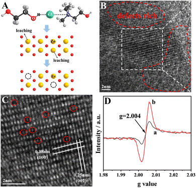
ZnO nanorod arrays were attached to a fluorine-doped tin oxide (FTO) substrate by a two-step method.19 As shown in Fig. 1A, surface zinc vacancies in the ZnO nanorod arrays were prepared through a novel strong-coordination leaching method with DES, which is a new class of green and sustainable solvent that can act as an effective leaching agent in the metal extraction process, even with a solid metallic compound.20,21 Specifically, the ZnO electrode was directly immersed in a DES solution to leach Zn atoms from ZnO lattices after being heated at different temperatures and for different amounts of time. After being optimized in DES, the ZnO electrodes exhibited the best PEC performance at 80 °C for 10 h (Fig. S1, ESI†).
 | ||
| Fig. 1 (A) Schematic diagram of Zn atoms leaching from ZnO lattices. HRTEM images (B and C) of Zn1−xO. (D) EPR spectra of ZnO (a) and Zn1−xO (b). | ||
The ZnO nanorod arrays had diameters of ≈150 nm and thicknesses of ≈1.5 μm (Fig. S1A and B, ESI†). Notably, the morphology of the ZnO electrode was unchanged after the defect etching, which maintained well the grain size and thickness of the pristine sample (Fig. S1C and D, ESI†). In addition, the XRD patterns could be readily indexed to the hexagonal structure of ZnO (JCPDS no. 74-0534) (Fig. S3, ESI†). No characteristic peaks of any other impurities were observed, indicating the high purity of the products.
To confirm the formation of Znvac, high-resolution transmission electron microscopy (HRTEM) of Zn1−xO was used. In the HRTEM image (Fig. S4A, ESI†), the lattice fringes of ZnO could be observed. The corresponding selected area electron diffraction (SAED) pattern displayed a spot pattern, indicating the single-crystalline character of the fabricated nanorods (Fig. S4B, ESI†). Intriguingly, both distinct and blurry lattice fringes were observed in the red frame region of Fig. 1B, implying that an abundance of Znvac existed on the surface of the ZnO.17,22 In addition, the magnified HRTEM image in Fig. 1C convincingly shows the presence of numerous vacancies. In this figure, the spacing values of the lattice fringes are 0.38 nm and 0.25 nm, corresponding to the (100) and (002) planes of wurtzite ZnO, which is in good agreement with the XRD results. Electron paramagnetic resonance (EPR) was also utilized to verify the existence of Znvac. As depicted in Fig. 1D, the samples had similar EPR signals (g = 2.004),17,23 and the different EPR signal intensities showed that the Zn1−xO possessed a higher concentration of Znvac compared with the intrinsic Znvac of ZnO. X-ray photoelectron spectroscopy (XPS) was also carried out (Fig. S5, ESI†). The O1s spectra of the DES-treated ZnO electrodes after 10 and 20 h exhibited a peak characteristic of absorbed oxygen, which could be considered as left behind after the formation of Znvac.24
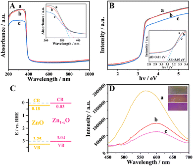
To investigate the light absorption and electronic structure of ZnO and Zn1−xO, further characterizations were carried out. The UV-vis diffuse reflection spectra show that the absorption edges of ZnO are around 389 nm, and Zn1−xO was slightly red-shifted relatively (Fig. 2A). The band gaps of ZnO and Zn1−xO were estimated to be 3.07 and 3.01 eV, respectively (Fig. 2B). To analyze the energy band structures of ZnO and Zn1−xO, electrochemical Mott–Schottky experiments were performed (Fig. S6, ESI†), and the calculated energy band positions of ZnO and Zn1−xO are schematically drawn in Fig. 2C following conversion. Compared to ZnO, the EVB and ECB of Zn1−xO are clearly increased and the band gap is reduced. The reduced band gap facilitates electron transfer from the VB to the CB.25 For the PEC reaction process, the shift of the band edges is conducive to the oxidation of water, thus consuming the holes left by the electron transition from the VB to the CB and reducing the recombination of electrons and holes.24 Room-temperature photoluminescence (PL) spectroscopy of ZnO and Zn1−xO was used to further certify the results (Fig. 2D). As shown in Fig. 2D, the PL emission intensities of the ZnO-450 °C and Zn1−xO are much lower than that of the ZnO, which suggests that the electron–hole pair recombination rate was suppressed effectively.26
The PEC performances of ZnO, ZnO-450 °C and Zn1−xO were evaluated using light illumination. As shown in Fig. S7 (ESI†), the Zn1−xO electrode possessed a photocurrent four times higher and a smaller resistance than ZnO, indicating that the presence of Znvac enhanced the interface charge transport process and promoted the photoelectric conversion. After treatment in DES the electrochemically active areas of the Zn1−xO electrode increased compared with ZnO-450 °C (Fig. S7C, ESI†).
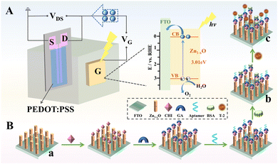
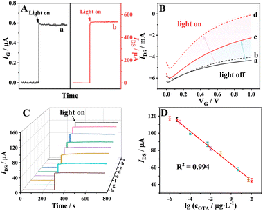
As shown in Scheme 1A, the Zn1−xO gate electrode was then integrated with a PEDOT:PSS channel-coated screen-printed carbon electrode to structure the OPECT device, which was preliminarily studied by measuring the channel current (IDS) and gate photocurrent (IG) responses upon illumination by a xenon lamp. Under illumination, Zn1−xO was excited to generate photoinduced electrons which moved from the valence band (VB) to the conduction band (CB), and then the electrons migrated to the FTO to form an anodic photocurrent, which gave a positive voltage to the channel. Under this positive voltage, the cation from the electrolyte will be inducted into the PEDOT:PSS channel, leading PEDOT to be de-doped, thus resulting in fewer carriers-holes in the channel. As a result, the IDS decreased as the photovoltage (Vphoto) and IG increased. Under illumination, the photocurrent absolute value of the gate electrode (IG = |IG,on − IG,off|) was ≈0.58 μA (Fig. 3A(a)) and the channel current absolute value of the channel electrode (IDS = |IDS,on − IDS,off|) was up to ≈535 μA (Fig. 3A(b)). Note that a small variation in IG of ≈0.58 μA gave rise to a considerable change in IDS of ≈535 μA.
 | ||
| Scheme 1 Schematic diagram of the response mechanism (A) and the construction (B) of the OPECT aptasensor. | ||
The Znvac gating effect on the OPECT aptasensor was further investigated. The typical transfer characteristics of the OPECT device were recorded to assess the capacity of the gate voltage (VG) to adjust IDS (Fig. 3B). The significant decrease of IDS as VG increased demonstrated a good modulation performance of the OPECT device. In addition, the ZnO gate electrode and Zn1−xO gate electrode exhibited different transfer character (black curves a and b) without illumination, whereas the two curves shifted in different manners toward lower VG upon illumination (red curves c and d). Specifically, with illumination, the transfer curve of the ZnO gate electrode shifted by a small amount to lower VG, while the Zn1−xO gate electrode shifted significantly, showing that the prepared OPECT aptasensor has an obvious gating effect because of Znvac. The same conclusion can be reached from Fig. S8A and B (ESI†). The Zn1−xO gate electrode produced a larger IDS than the ZnO-450 °C and ZnO electrodes (Fig. S8A, ESI†), corresponding to the largest IG (Fig. S8B, ESI†). This indicates that Zn1−xO can generate a large photovoltage, which can control the voltage range and achieve high sensitivity detection in the OPECT system.
An OPECT aptasensor was then constructed (Scheme 1B) using the synthetic Zn1−xO as the gate electrode and an aptamer as the recognition element. First, aldehyde groups for Zn1−xO were introduced by chitosan (CHI) and glutaraldehyde (GA) in a controlled fashion, after which the amidogen-containing aptamer was connected. The aptamer was anchored by an aldimine condensation reaction on the Zn1−xO electrode. An evident decrease of IDS could be observed after immobilizing the aptamer, causing a decrease in IG (Fig. S9A, ESI†), which was put down to the large resistance of the aptamer.27 The same result can be concluded from curve b of Fig. S9B (ESI†); the steric hindrance of the electrode interface was increased after modifying the aptamer.28 Then, bovine serum albumin (BSA) was used to block the superfluous aldehyde group. Then fabrication of this aptasensor was accomplished. The aptasensor could specifically recognize and capture OTA toxin, which hindered the transfer of electrons. As a consequence, the IDS decreased and the value of the electron transfer resistance (Ret) increased further (Fig. S9A and B, ESI†). Therefore, the signal changes arising from the specific binding of the aptamer and OTA can result in the quantitative detection of the OTA toxin.
The OPECT aptasensor has a good response to OTA under the optimal experimental conditions previously mentioned (Fig. S10, ESI†). As shown in Fig. 3C, the IDS responses decreased gradually with increasing concentration of OTA, indicating that the IG responses are suppressed by OTA on the biointerface. A good linear relationship with a regression equation of IDS = 63.89 − 9.58[lg![[thin space (1/6-em)]](https://www.rsc.org/images/entities/char_2009.gif) COTA (μg L−1)] (R2 = 0.994) can be derived for the detection of the OTA concentration ranging from 5 pg L−1 to 50 μg L−1 and the detection limit was experimentally found to be 1.66 pg L−1 (S/N = 3), as shown in Fig. 3D.
COTA (μg L−1)] (R2 = 0.994) can be derived for the detection of the OTA concentration ranging from 5 pg L−1 to 50 μg L−1 and the detection limit was experimentally found to be 1.66 pg L−1 (S/N = 3), as shown in Fig. 3D.
To investigate the selectivity of the fabricated OPECT aptasensor, ochratoxin A (OTA), ochratoxin B (OTB), ochratoxin C (OTC), aflatoxin B1 (AFB1), T-2 toxin (T-2), and their mixture were employed as interferents. 100 pg L−1 of these interferents did not lead to significant alteration of IDS compared with 10 pg L−1 of OTA and their mixture, indicating excellent selectivity of the constructed OPECT aptasensor for OTA detection (Fig. S11A, ESI†). Furthermore, the signal decreased by nearly 4.5% after several on/off illumination cycles within 1000 s, indicating the photocurrent signal of Zn1−xO was quite stable for the detection (Fig. S11B, ESI†). After the Zn1−xO electrode had been stored at 4 °C for 20 days, the IDS signal maintained 95% of the initial response, indicating considerable robustness and long-term storage stability (Fig. S11C, ESI†).
The potential for practical application of the OPECT aptasensor was explored by detecting different concentrations of OTA in corn flour samples using the standard addition method. The pretreatment of the corn flour was according to a previously reported method.29 As shown in Table S1 (ESI†), the recoveries are in the range of 95.7% to 100.2% and the relative standard deviation (RSD) varied from 3.6% to 6.3%, clearly indicating that this platform has satisfactory applicability for the detection of OTA in real samples. Furthermore, compared with other published reports as shown in Table S2 (ESI†), this sensor platform has a wider detection range and lower detection limit.
In summary, we successfully introduced surface Znvac into ZnO nanorod arrays using a novel strong solvent coordination leaching method. HRTEM images, EPR spectra and XPS spectra demonstrate the introduction of Znvac. In addition, PL spectra, EIS Nyquist plots and photocurrent results revealed that the presence of Znvac on the surface notably accelerates the electron–hole separation, enhances the interface charge transport process and promotes the photoelectric conversion. The Zn1−xO electrode with excellent PEC performance as a photo-gate electrode was used to design a highly efficient OPECT device which showed a three orders of magnitude increase in the channel response and a good performance for OTA determination. Given these results, engineering metal defects on a surface is a new avenue for photoactive material design with high PEC performance. Additionally, this work has successfully developed a promising pathway in the electrochemical field for high sensitivity sensing devices with a wider range of applications.
This work was supported by Key R&D Program of Jiangsu Province (No. BE2020677); National Natural Science Foundation of China (No. 22174055).
Conflicts of interest
There are no conflicts to declare.Notes and references
- J. Song, P. Lin, Y. F. Ruan, W. W. Zhao, W. Wei, J. Hu, S. Ke, X. Zeng, J. J. Xu, H. Y. Chen, W. Ren and F. Yan, Adv. Healthcare Mater., 2018, 7, e1800536 CrossRef.
- L. Ding, Y. Liu, J. Lai, W. Zhu, C. Fan, N. Hao, J. Wei, J. Qian and K. Wang, Adv. Funct. Mater., 2022, 32, 2202735 CrossRef CAS.
- J. Hu, M. J. Lu, F. Z. Chen, H. M. Jia, H. Zhou, K. Li, X. Zeng, W. W. Zhao and P. Lin, Adv. Funct. Mater., 2022, 32, 2109046 CrossRef CAS.
- Y. T. Xu, Z. Li, C. Yuan, J. Q. Wu, J. Hu, P. Lin, W. W. Zhao, H. Y. Chen and J. J. Xu, Adv. Opt. Mater., 2022, 10, 2102687 CrossRef CAS.
- K. Feng, W. Shan, S. Ma, Z. Wu, J. Chen, H. Guo, B. Liu, J. Wang, B. Li, H. Y. Woo, S. Fabiano, W. Huang and X. Guo, Angew. Chem., Int. Ed., 2021, 60, 24198–24205 CrossRef CAS PubMed.
- A. Nawaz, Q. Liu, W. L. Leong, K. E. Fairfull-Smith and P. Sonar, Adv. Mater., 2021, 33, 2101874 CrossRef CAS.
- L. Wang, X. Q. Cui, Y. T. Xu, M. Anpo and Y. X. Fang, Chem. Commun., 2022, 58, 10469–10479 RSC.
- Y. Q. Qu and X. F. Duan, Chem. Soc. Rev., 2013, 42, 2568–2580 RSC.
- F. E. Osterloh, Chem. Soc. Rev., 2013, 42, 2294–2320 RSC.
- S. Liu, Z. R. Tang, Y. Sun, J. C. Colmenares and Y. J. Xu, Chem. Soc. Rev., 2015, 44, 5053–5075 RSC.
- J. Li, S. K. Cushing, P. Zheng, F. Meng, D. Chu and N. Wu, Nat. Commun., 2013, 4, 2651 CrossRef PubMed.
- G. Wang, Y. Ling and Y. Li, Nanoscale, 2012, 4, 6682–6691 RSC.
- M. Guan, C. Xiao, J. Zhang, S. Fan, R. An, Q. Cheng, J. Xie, M. Zhou, B. Ye and Y. Xie, J. Am. Chem. Soc., 2013, 135, 10411–10417 CrossRef CAS.
- S. Wang, X. Wang, B. Liu, Z. Guo, K. K. Ostrikov, L. Wang and W. Huang, Nanoscale, 2021, 13, 17989–18009 RSC.
- H. Yu, J. Li, Y. Zhang, S. Yang, K. Han, F. Dong, T. Ma and H. Huang, Angew. Chem., Int. Ed., 2019, 58, 3880–3884 CrossRef CAS.
- L. Lu, B. Wang, S. Wang, Z. Shi, S. Yan and Z. Zou, Adv. Funct. Mater., 2017, 27, 1702447 CrossRef.
- Y. Q. He, H. Rao, K. P. Song, J. X. Li, Y. Yu, Y. Lou, C. G. Li, Y. Han, Z. Shi and S. H. Feng, Adv. Funct. Mater., 2019, 29, 1905153 CrossRef CAS.
- Y. Zhi, Y. Yi, C. Deng, Q. Zhang, S. Yang and F. Peng, ChemSusChem, 2022, 15, e202200860 CrossRef CAS PubMed.
- J. Wei, W. Chang, A. Qileng, W. Liu, Y. Zhang, S. Rong, H. Lei and Y. Liu, Anal. Chem., 2018, 90, 9606–9613 CrossRef CAS PubMed.
- M. K. Tran, M. T. F. Rodrigues, K. Kato, G. Babu and P. M. Ajayan, Nat. Energy, 2019, 4, 339–345 CrossRef CAS.
- K. Rong, L. Huang, H. Zhang, J. F. Zhai, Y. X. Fang and S. J. Dong, Chem. Commun., 2018, 54, 8853–8856 RSC.
- X. Hao, J. Zhou, Z. Cui, Y. Wang, Y. Wang and Z. Zou, Appl. Catal., B, 2018, 229, 41–51 CrossRef CAS.
- A. B. Djurišić, W. C. H. Choy, V. A. L. Roy, Y. H. Leung, C. Y. Kwong, K. W. Cheah, T. K. Gundu
![[thin space (1/6-em)]](https://www.rsc.org/images/entities/char_2009.gif) Rao, W. K. Chan, H. Fei
Rao, W. K. Chan, H. Fei![[thin space (1/6-em)]](https://www.rsc.org/images/entities/char_2009.gif) Lui and C. Surya, Adv. Funct. Mater., 2004, 14, 856–864 CrossRef.
Lui and C. Surya, Adv. Funct. Mater., 2004, 14, 856–864 CrossRef. - Y. Lu, Y. L. Yang, X. Y. Fan, Y. Q. Li, D. H. Zhou, B. Cai, L. Y. Wang, K. Fan and K. Zhang, Adv. Mater., 2022, 34, 2108178 CrossRef CAS.
- M. Zhang, Z. Zhang, J. Wei, Z. Dai, N. Hao and K. Wang, Chem. Commun., 2021, 57, 5973–5976 RSC.
- X. Li, S. Fang, L. Ge, C. Han, P. Qiu and W. Liu, Appl. Catal., B, 2015, 176, 62–69 CrossRef.
- L. J. Ding, J. Wei, Y. Qiu, Y. Wang, Z. R. Wen, J. Qian, N. Hao, C. F. Ding, Y. Q. Li and K. Wang, Chem. Eng. J., 2021, 407, 127213 CrossRef CAS.
- Z. L. Han, J. N. Shu, X. Liang and H. Cui, Anal. Chem., 2019, 91, 12260–12267 CrossRef CAS PubMed.
- J. Wei, Q. Hu, Y. Gao, N. Hao, J. Qian and K. Wang, Anal. Chem., 2021, 93, 6214–6222 CrossRef CAS.
Footnote |
| † Electronic supplementary information (ESI) available. See DOI: https://doi.org/10.1039/d2cc05735b |
| This journal is © The Royal Society of Chemistry 2023 |


