Broadband perfect optical absorption enabled by quasi-bound states in the continuum in graphene non-concentric rings
Kun
Xu
,
Jianyuan
Huang
and
Weihua
Wang
 *
*
School of Material Science and Physics, China University of Mining and Technology, Xuzhou 221116, People's Republic of China. E-mail: wh.wang@outlook.com
First published on 22nd November 2022
Abstract
Graphene plasmons, possessing a lot of unique optical properties, have been employed to enable a variety of applications in the THz frequency range. Here, we demonstrate bound states in the continuum (BICs), electromagnetically induced transparency (EIT)-like effects, high-performance broadband optical absorption (OA), and narrow-band OA in a square lattice of graphene non-concentric rings (GNCRs). We show that due to inversion symmetry breaking, the symmetry-protected BICs will evolve into quasi-BICs as the eccentricity of GNCRs becomes nonzero, manifested itself as a new resonance dip appearing in the transmission spectrum. The observation can be well described by a coupled-oscillator model, namely, the coupling between a dipole state and a quadrupole state. Besides, as the eccentricity becomes very large, the structure can also support EIT-like effects, in which a transparency window will occur at the frequency of the original transmission dip caused by the dipole state, and the transmission spectrum turns into a typical W-shape. Based on the idea of BICs, we propose a broadband terahertz (THz) perfect OA by using the typical sandwiched structure, namely, with the configuration of the GNCR layer-spacer layer-metal layer. Full wave simulations are performed, which show that the OA of over 90% absorptance can be achieved at frequencies from 0.67 THz to 1.66 THz, and over 99% absorptance can be achieved at frequencies from 1.24 THz to 1.49 THz. In the absorption band, three peaks come from three graphene plasmonic modes, which are two dipole resonances and a quadrupole resonance induced by symmetry breaking. Moreover, the perfect OA performance can be well maintained for oblique incidences of transverse electric polarization, with an incidence angle of up to 30°. Finally, we show that the broadband perfect OA can be switched to narrowband perfect OA, and its operating frequency can be continuously tuned by changing the Fermi level. Our results will promote the development of graphene-based applications in THz and infrared regimes.
1. Introduction
Optical absorption (OA) is one of the most important aspects of light-matter interaction. However, due to its unique one-atom thickness, two-dimensional (2D) graphene hosts a rather small OA, e.g. a general 2.3% absorptance over a broad visible region.1 To enhance OA in graphene, a scheme via periodically patterned structures is commonly implemented, by which maximum 50% absorptance is achieved.2–4 The crucial factor of this approach is the local resonances strongly bound to structured graphene, also known as graphene plasmons.5–7 In contrast to plasmons in three-dimensional (3D) noble metals, they exhibit significant advantages in field confinement and propagation,8–10 and more remarkably, their resonance frequencies lying in the terahertz (THz) and/or infrared region can be tuned dynamically through electrostatic gating,11,12 static magnetic field,13–16 and mechanical folding.17–19 By placing a metal reflector, sharing an identical idea of metal–insulator–metal (MIM) designs, graphene plasmons can achieve exact 100% OA at plasmonic resonance frequencies,20–22 thus achieving narrowband complete OA. However, because of the discrete feature of these frequencies, it is quite challenging to engineer broadband complete OA in plasmonic systems, where a basic trade-off occurs between absorption efficiency and bandwidth. In principle, extra mechanisms should be incorporated to improve the absorption bandwidth, e.g. spanning the frequency range via multiple modes.23–25 On the other hand, the complete OA can be well interpreted by considering the different contributions of radiative loss and internal loss, or equivalently, the competitive relationship between two kinds of Q-factors.26 Recently, the bound states in the continuums (BICs) were demonstrated, which remain localized even though they are embedded in the continuum of extend states, sometimes referred to as embedded eigenvalues.27,28 BICs exhibit very strong abilities to modulate Q-factors of the local resonances and thus can be applied to the designs of high OA.The BICs can be classified into two distinct types, namely, an ‘accidental’ BIC and a symmetry-protected BIC.29 To engineer the former, the parameters of the target system should be tuned to achieve destructive interference of outgoing waves,30–32 while for the latter, a trapped mode compatible with the free-space radiation should be designed with a different symmetry than that of radiation.33–35 In the absence of the internal damping channel (e.g. using materials without imaginary parts in the permittivity), the leakage of energy is solely determined by the radiating channel, which can be blocked to achieve true BICs, through the two scenarios mentioned above. However, the two implementations are generally different in complexity, e.g. the symmetry-protected BICs are easier to be realized and, with more flexibility. A common treatment is to build the unit cell with two identical resonators,36–41 where the antisymmetric (dark) mode will be exactly hidden in the flat transmission spectrum. To identify these BICs, the evolution of the bound states can be tracked by breaking the symmetry by fine-tuning the shape, size, and orientation of either one of the two resonators. In the procedure, the true BICs will turn to quasi-BICs with high, yet finite Q-factor. It is worth noting that the behavior can be well described by the Fano formula, and the Q-factor is inversely proportional to the square of the asymmetry parameter.42 In the presence of the internal damping channel, e.g. in lossy plasmonic structures,43,44 the Q-factor is limited but can still be improved by applying the idea of BICs, thus meeting the particular requirements of enhanced plasmonic OA.
In this article, we propose broadband perfect OA based on symmetry-protected BICs. The structure is made of a square lattice of graphene nonconcentric rings (GNCRs). In graphene circular rings, a BIC is completely embedded in the transmission spectrum which is dominated by an absorption dip caused by the dipole resonance; in GNCRs, because symmetry breaking appears, the BIC evolves into quasi BICs, manifested as a new resonance dip in the spectrum. We show that by using such a single layer of GNCRs, the OA of over 90% absorptance is achieved at the frequencies from 0.67 THz to 1.66 THz, with a fractional bandwidth of 85.0%. Besides, at the frequencies from 1.24 THz to 1.49 THz, nearly complete OA (over 99% absorptance) is obtained. Such an OA performance can remain even for oblique incidence with the incident angle up to 30° for transverse electric (TE) polarization. Finally, we show that such broadband perfect OA can be converted to narrowband perfect OA by raising the Fermi level of graphene.
2. Design and theoretical model
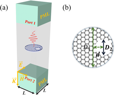
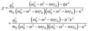
The system under study is a graphene plasmonic crystal with a square lattice, and its unit cell is graphene nonconcentric ring as schematically depicted in Fig. 1. In practice, the geometric parameters are the first set as follows: the diameter of disk D1 = 36 μm, the diameter of the hole D2 = 14 μm, the eccentricity d = 10.95 μm, and the periodicity L = 48 μm. The whole structure is embedded in a homogeneous medium of a dielectric constant εr. Without the loss of generality, air (εr = 1) is chosen as the medium in the BICs studies, and Si (εr = 2.35) is chosen as the medium in the perfect OA studies. In order to excite BICs, the incident electric field is fixed along the y direction (namely, TE polarization) throughout this work.As well known, the eigenmodes of a plasmonic system are a set of self-standing electromagnetic excitations with different resonance frequency ω and damping rate γ. Through structural modulation, the coupling between them can occur, which might be employed to make high-Q resonances (quasi-BICs) and BICs.45 Here, the involved resonances are a dipole and a quadrupole, and their coupling can be simply described by a model of two coupled harmonic oscillators,19,46 as presented in a matrix form.
 | (1) |
Practically, the evolution of quasi-BICs can be described quantitatively by deriving an analytical formula of the transmission spectrum from eqn (1). By calculating the displacement xD/Q of two oscillators,19 their susceptibility defined as χ = (qDxD + qQxQ)/E0 can be readily written down as
 | (2) |
The presented coupled-oscillator model is not limited to a specific material, as long as the local resonances follow the Lorentz formula. However, the light-matter interaction in each material will be characterized by their own dielectric functions. As usual, the optical response of the graphene layer is treated at the macroscopic level, via its homogeneous surface conductivity (ω) as given by36
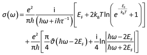 | (3) |
![[thin space (1/6-em)]](https://www.rsc.org/images/entities/char_2009.gif) 000 cm2 V−1 s−1 in the following studies, except where noted. The setting values of these two parameters are not uniquely determined, and in practice, a lower Fermi level can be applied when a larger carrier mobility is used, or vice versa.
000 cm2 V−1 s−1 in the following studies, except where noted. The setting values of these two parameters are not uniquely determined, and in practice, a lower Fermi level can be applied when a larger carrier mobility is used, or vice versa.
To demonstrate BICs explicitly, full wave simulations are performed using finite element software COMSOL, in which the 2D graphene sheet is modelled as a very thin 3D conducting film with an artificial thickness tg. Accordingly, the bulk dielectric function is able to be expressed as ε(ω) = ε0 + iσ(ω)/(ωtg). The convergence of simulations is confirmed as adopting a sufficiently small thickness tg, which is set to be 0.5 nm with a good numerical accuracy and efficiency. The detailed modelling of the periodic plasmonic system is illustrated in Fig. 1. The GNCR is placed at the center of the simulation domain that is truncated with four periodic boundary conditions (PBCs) and two ports. The perfectly matched layer (PML) is used to prevent two ports from redundant reflections. A plane wave with an electric field along the y direction is normally incident from port 1 and then received at port 2. As a result, the transmission spectrum is directly extracted from the built-in S parameters, e.g. T = |S21|2, and similarly, the reflection spectrum is given by R = |S11|2.
3. Results and discussion
We first calculate transmission spectra for different eccentricity d. As show in Fig. 2(a), when d = 0 μm, the transmission spectrum possesses a well-defined Lorentz shape, with only one transmission dip. As d = 4 μm, the lateral inversion symmetry is broken, and a new transmission dip emerges at higher frequency and with a relatively narrow bandwidth (equivalently, very high Q-factor). As compared to the spectrum of d = 0 μm, this new dip is completely embedded and can be excited as breaking the lateral inversion symmetry, which is an important stamp of BICs. From this point of view, this state is a true BIC as d = 0 μm, and turns into a quasi-BIC as d = 4 μm. As d further increases, this new transmission dip experiences a gradual redshift and bandwidth broadening. Meanwhile, the original transmission dip shows a slight redshift, and its linewidth and resonance strength are reduced, which are more clearly displayed in Fig. 2(b). It is also seen that the two states are competitive in the transmission spectra.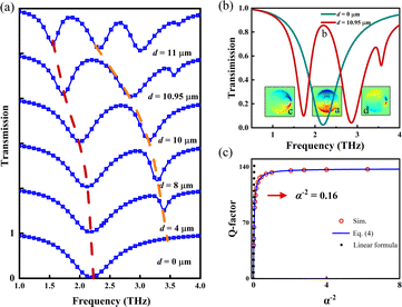 | ||
| Fig. 2 (a) Transmission spectra at different eccentricity d, which are obtained from full wave simulation. (b) The demonstration of the EIT effect (red curve) as d = 10.95 μm. The green curve shows the transmission spectrum as d = 0 μm. The insets give the field patterns of three modes at three transmission dips. (c) Q-factor of quasi-BICs as a function of quantity α−2, with the asymmetry parameter α = d/(1 μm). The circles are obtained from simulations, and the curve is plotted from eqn (4). The black dots present the linear formula. | ||
Besides BICs, there is also another very interesting effect, which is shown in Fig. 2(b). It is seen that as compared to the spectrum of d = 0 μm, the original transmission dip (roughly zero transmission) will turn to a transparency window as d = 10.95 μm, and the transmission spectrum exhibits a typical W-shape. This observation is quite similar to the well-known electromagnetically induced transparency (EIT).47–49 To figure out the mechanism behind, we exact the field patterns at the three transmission dips. It is very clear that as d = 0 μm, the original transmission dip (marked by a) is caused by a dipole resonance; as d = 10.95 μm, the two transmission dips result from a dipole resonance (marked by c) and a quadrupole resonance (marked by d), respectively. Here, the dipole acts as the bright state, and the quadrupole plays the role of the dark state. The interaction between them, namely, bright-dark mode interaction, leads to the EIT-like effect.
Another important tag of BICs is their divergent Q-factor in lossless systems. It is worth evaluating Q-factor (Q = ω/2γ) in such a lossy plasmonic system. As demonstrated by Koshelev et al.,50 the Q-factor for quasi-BICs can be represented as a simple linear formula of the inverse square of the asymmetry parameter, which can be considered as a general result for symmetry-protected BICs. We here follow this work, by defining α = d/(1 μm) as the asymmetry parameter and then find the relationship between Q-factor and α−2. The results are summarized as shown in Fig. 2(c) (the red circles). It is seen that for smaller α−2, e.g. α−2 ≤ 0.16 (corresponding to d ≥ 2.5 μm) as indicated by the arrow, Q-factor is well described by the linear formula (black dotted lines in Fig. 2 (c));50 however, it deviates from the linear formula for larger α−2.
The deviation must be from the intrinsic loss of graphene, because the linear formula is derived in dielectric systems, in which there is no intrinsic loss. The Q-factor can be represented as Q−1 = Qi−1 + Qr−1 and we can simply replace Qr by Qrα−2, with the prefactor Qr being a constant. Accordingly, the formula for the total Q-factor is given by19
 | (4) |
To get a comprehensive understanding of the observation, we employ the coupled-oscillator model as given by eqn (1) and (2). To avoid redundancy, we will only study the case as d = 10.95 μm. In practice, all the eigenstates supported by the structure can be rigorously computed based on the eigenvalue analysis module in COMSOL. By comparing the transmission spectrum, the involved modes can be easily identified, e.g. the dipole and the quadrupole as shown in Fig. 2(b). Then, using the resonance frequency ω and damping rate γ for these two modes, and adopting an eccentricity d dependent coupling strength κ, we are able to calculate the transmission spectrum. The numerical results are shown as the red dotted curve in Fig. 3, which are in good agreement with the simulation result (blue dotted curve). This agreement indicates clearly that the symmetry-protected BICs here are the quadrupole state embedded in the spectrum dominated by the dipole state; by breaking the inversion symmetry, the quadrupole state evolves into quasi-BICs with a high Q-factor, along with a new transmission dip. By further increasing d, the frequency difference between the dipole and the quadrupole states is reduced, which will cause a significantly strong coupling between them and also the EIT-like effect, as interpreted by the model.
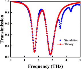 | ||
| Fig. 3 Transmission spectra as the eccentricity d = 5.45 μm, the blue dotted curve and red dotted curve are obtained from full wave simulation and the coupled-oscillator model given by eqn (2), respectively. Here, ωD = 1.74 THz, ωQ = 2.86 THz, γD = 0.34 THz, γQ = 0.76 THz, κ = 0.87 THz, qD = 2.20, qQ = 3.76, and mD = mQ = 19.8. | ||
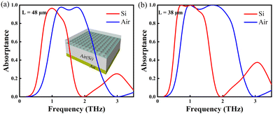
As well known, due to its intrinsic loss, graphene can also be used to design perfect OA, especially in the THz regime, namely the perfect THz absorber. So, as usual, we employ the general MIM design (see the inset in Fig. 4(a)), in which the top layer is the square lattice of GNCRs, the medium layer is a dielectric (e.g. air or silicon), and the bottom is an optically thick gold layer used to prevent wave transmission. This is a typical one-port, reflection-type absorber. In practice, we first adopt the parameters for GNCRs as in the above BIC studies, e.g. D1 = 36 μm, D2 = 14 μm, d = 10.95 μm, and L = 48 μm, but the Fermi level EF = 0.3 eV, and the thickness of the medium layer is set to be t = 50 μm. The simulation results are shown in Fig. 4(a). It is seen that the broadband perfect OA (over 90% absorptance) is achieved, and the dielectric with smaller permittivity (e.g. the blue curve for air) will result in better performance such as a broader bandwidth. By making a more compact lattice, without changing GNCRs, but reducing only their spacing, e.g. from L = 48 μm to L = 38 μm, the perfect OA bandwidth and efficiency will be greatly improved. As shown in Fig. 4(b), the OA of over 90% absorptance is achieved at the frequencies from 0.9 THz to 2.1 THz. However, it can only realize over 90% absorptance from 0.6 THz to 1.4 THz when the medium air is replaced by silicon.
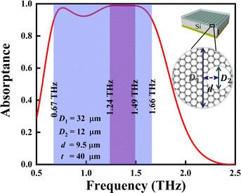
To further improve the OA performance, we can optimize the structural parameters of GNCRs, which are given as follows: D1 = 32 μm, D2 = 12 μm, d = 9.5 μm, L = 34 μm, t = 40 μm, EF = 0.3 eV, μ = 10![[thin space (1/6-em)]](https://www.rsc.org/images/entities/char_2009.gif) 000 cm2 V−1 s−1, and silicon as the medium. These parameters will be used in the following studies, unless otherwise specified. The simulation results are shown in Fig. 5. It is seen that both the absorption efficiency and bandwidth are greatly improved. The OA of over 90% absorptance is achieved at the frequencies from 0.67 THz to 1.66 THz, and especially, nearly complete OA (e.g. over 99% absorptance) is obtained at the frequencies from 1.24 THz to 1.49 THz. In contrast, either graphene rings (black curve) or graphene disks (blue curve) with the same structural parameters and Fermi level, exhibit much weaker OA in both absorption efficiency and bandwidth.
000 cm2 V−1 s−1, and silicon as the medium. These parameters will be used in the following studies, unless otherwise specified. The simulation results are shown in Fig. 5. It is seen that both the absorption efficiency and bandwidth are greatly improved. The OA of over 90% absorptance is achieved at the frequencies from 0.67 THz to 1.66 THz, and especially, nearly complete OA (e.g. over 99% absorptance) is obtained at the frequencies from 1.24 THz to 1.49 THz. In contrast, either graphene rings (black curve) or graphene disks (blue curve) with the same structural parameters and Fermi level, exhibit much weaker OA in both absorption efficiency and bandwidth.
It is quite interesting that by shifting the hole of the ring to its edge, the OA performance can be improved significantly both in absorption efficiency and bandwidth. This exactly coincides with the physics of BICs. Because of the shifting, the inversion symmetry is broken, and therefore the quasi-BICs that are completely embedded in the spectra of the symmetric rings, will play an important role in the OA. This is easy to be confirmed by checking the local resonances which are involved in the OA. As shown in Fig. 6(a), there are two local maxima (namely, peaks, marked by blue and black circles, respectively) in the OA spectra of graphene disks and rings, while there are three peaks (marked by red circles) in the OA spectrum of GNCRs. The field patterns of these peaks are shown in Fig. 6(b). In graphene disks and rings, the two peaks are contributed by two kinds of dipole resonances. The local fields of the lower frequency resonances at 0.83 THz and 0.77 THz are strongly bound to the edges, while those of the higher frequency resonances at 1.65 THz and 1.37 THz spread much more to the bulk. This phenomenon is very clear in graphene rings. In GNCRs, the two lower frequency peaks locating at 0.76 THz and 1.30 THz, with these frequencies very close to those of graphene rings, are still caused by the dipole resonances. For the 0.76 THz state, the local fields are bound partly to the outer edge and partly to the inner edge of the hole. The highest frequency peak at 1.47 THz originates from a quadruple resonance. There is a very strong yet small hotspot located in the narrow region between the outer edge and the inner edge of the hole, which can be considered to be from the strong interaction between these two edges. Clearly, in the absence of this hotspot, the quadrupole will be reduced to a dipole.
Since the extent of symmetry breaking depends on the eccentricity d, it is worth evaluating the dependence of OA on d. The simulation results are shown in Fig. 6(c). It is seen that for smaller d, e.g. d ≤ 4 μm, the OA spectrum remains almost the same; by further increasing d, the higher frequency OA peak at around 1.47 THz occurs gradually, and finally, as d ≥ 8 μm, it will merge with the lower frequency peak to form broadband high performance OA, e.g. over 90% absorptance. When the hole is very close to the outer edge, e.g. d → (D1 − D2)/2 = 10 μm, the OA of over 99% absorptance can also be achieved at around the frequency of the quadrupole state.
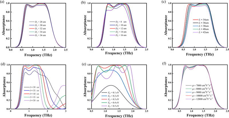
Based on the above parameters, we can investigate the evaluation of OA performance by varying only one of these parameters. However, when varying D1 and D2, we do not take a constant d; instead, we set d + 0.1 = (D1 − D2)/2, namely, the distance between the outer edge and the edge of hole is constant 0.1 μm. As shown in Fig. 7(a), with decreasing D1, the lower frequency OA peak undergoes a slight redshift, while more importantly, the OA at higher frequencies is strongly suppressed. By increasing D2 from 12 μm to 16 μm, the OA bandwidth and the absorptance at the lower frequency are clearly reduced (see Fig. 7(b)); as D2 decreases from 12 μm to 8 μm, the OA bandwidth seems to be improved but the absorption efficiency is greatly reduced at the frequency around 1.00 THz. So, it is more like two narrowband perfect OA.
By increasing L from 34 μm to 42 μm (see Fig. 7(c)), both the OA bandwidth and efficiency are reduced gradually. It is clear that the influence of L on OA is much smaller than D1 and D2. As compared to L, the thickness t of the medium layer is more important, because the medium layer together with the bottom gold layer forms a Fabry–Perot (FP) resonant cavity, which plays a key factor in broadband OA.51–53 As shown in Fig. 7(d), by increasing t or decreasing t, the OA performance will be reduced significantly, in both absorption bandwidth and efficiency. Besides these structural parameters, two material parameters of graphene are also essential to the OA performance. As shown in Fig. 7(e), as EF deviates from 0.3 eV, the OA spectra will become very fluctuating, and when EF = 0.2 eV or 0.1 eV, the absorptance is reduced rapidly. In contrast, as shown in Fig. 7(f), the OA spectrum exhibits a relatively weak dependence on carrier mobility μ, e.g. as μ increases from 7000 cm2 V−1 s−1 to 12![[thin space (1/6-em)]](https://www.rsc.org/images/entities/char_2009.gif) 000 cm2 V−1 s−1, the overall changes of absorption bandwidth and efficiency are rather limited.
000 cm2 V−1 s−1, the overall changes of absorption bandwidth and efficiency are rather limited.
For practical applications, the robustness of perfect OA performance is of great importance. Previously, only the case when the wave is normally incident is considered. Thus in Fig. 8, we show the dependence of OA on incidence angle θ of oblique incidence. As usual, it is inevitable that the absorption performance will be reduced as θ increases. Over 90% and broadband absorption can survive as the angle θ up to 30° (marked by the black curve). Moreover, it should be mentioned that over 90% absorptance at higher frequencies will be maintained as the angle θ up to 80°. This results in a narrowband POA, and its operating frequency undergoes a gradual blueshift as θ increases.
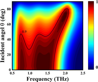 | ||
| Fig. 8 Absorptance of GNCRs as the TE polarized wave obliquely incident with incident angle θ. The black curve marks the region in which the absorptance is larger than 0.9. | ||
Finally, as shown in Fig. 7(e), the Fermi level can affect the OA performance dramatically. In fact, the Fermi level can also be applied to switch the functionality of such a structure. This could be one of the important advantages of graphene plasmonic devices. For broadband OA, the optimized Fermi level is 0.3 eV, and we here show that this broadband OA can be switched to a narrowband OA with its operating frequency continuously tuned by the Fermi level, equivalently, electrostatic gating. The simulation results are shown in Fig. 9. It is clearly seen that with increasing EF from 0.6 eV to 1.0 eV, the broadband OA does not appear, and the narrowband POA undergoes a gradual blueshift from 1.50 THz to 1.82 THz. It is also worth noting that as EF = 0.6 eV, a dual narrowband complete OA is achieved at 1.50 THz and 2.00 THz.
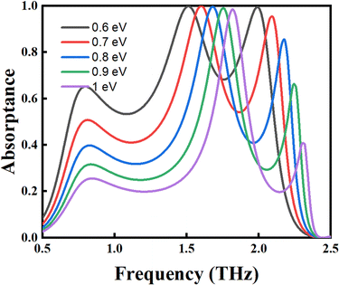 | ||
| Fig. 9 Absorption spectra as the Femi level increases from 0.6 eV to 1.0 eV. Narrowband nearly complete OA is observed with continuously tuned operating frequency. | ||
Conclusions
To summarize, we demonstrate symmetry-protected BICs in graphene rings, and they will evolve into quasi-BICs as the rings are converted to nonconcentric rings, manifested as a new resonance dip in the transmission spectrum. The deviation is characterized by the eccentricity d, which is related to the asymmetry parameter α through α = d/(1 μm). Besides, we develop a general formula to describe the Q-factor of quasi-BICs, which is different from the linear formula in dielectric systems. As α−2increases, the Q-factor first increases linearly and is then saturated to a constant Q-factor determined by the material loss. We show that the proposed structure can also support EIT-like effects, which behaves like a switch between BIC (d = 0 μm) and EIT (d = 10.95 μm). Finally, we use the proposed structure, a square lattice of GNCRs, to design broadband perfect OA at THz frequencies. The typical design of the three-layer sandwiched configuration is employed, consisting of a GNCR layer, a dielectric spacer layer, and a gold bottom layer. By using the optimized structural parameters, broadband perfect OA (over 90% absorptance) can be achieved at frequencies from 0.67 THz to 1.66 THz, with a fractional bandwidth of 85.0%. (0.67–1.66THz, over 90% absorptance), which can be interpreted as the interplay between three graphene plasmonic resonances, with the largest frequency being that of the quasi-BICs. At frequencies close to the three resonances, nearly 100% absorptance can be reached. Moreover, we show that broadband perfect OA can be maintained for the oblique incidence with an incident angle up to 30°. Finally, the broadband perfect OA can be switched into a narrowband POA as Fermi level EF > 0.5 eV, and particularly, its operating frequency can be continuously tuned by varying EF.Conflicts of interest
There are no conflicts to declare.Acknowledgements
This work was financially supported by the National Natural Science Foundation of China (NSFC) (Grant No. 12174440).References
- R. R. Nair, P. Blake, A. N. Grigorenko, K. S. Novoselov, T. J. Booth, N. M. R. Peres and A. K. Geim, Science, 2008, 320, 1308 CrossRef CAS PubMed.
- Z. Fang, Y. Wang, A. E. Schlather, Z. Liu, P. M. Ajayan, F. J. Garcia de Abajo, P. Nordlander, X. Zhu and N. J. Halas, Nano Lett., 2014, 14, 299–304 CrossRef CAS PubMed.
- T. Stauber, G. Gomez-Santos and F. J. Garcia de Abajo, Phys. Rev. Lett., 2014, 112, 077401 CrossRef CAS PubMed.
- M. Jablan and D. E. Chang, Phys. Rev. Lett., 2015, 114, 236801 CrossRef PubMed.
- B. Wunsch, T. Stauber, F. Sols and F. Guinea, New J. Phys., 2006, 8, 318 CrossRef.
- E. H. Hwang and S. Das Sarma, Phys. Rev. B: Condens. Matter Mater. Phys., 2007, 75, 205418 CrossRef.
- M. Jablan, H. Buljan and M. Soljacic, Phys. Rev. B: Condens. Matter Mater. Phys., 2009, 80, 245435 CrossRef.
- J. Christensen, M. Alejandro, S. Thongrattanasiri, F. Koppens and F. J. Garcia de Abajo, ACS Nano, 2012, 6, 431–440 CrossRef CAS.
- F. Koppens, D. E. Chang and F. J. Garcia de Abajo, Nano Lett., 2011, 11, 3370–3377 CrossRef CAS PubMed.
- T. Low and P. Avouris, ACS Nano, 2014, 8, 1086–1101 CrossRef CAS PubMed.
- J. Chen, M. Badioli, P. Alonso-Gonzalez, S. Thongrattanasiri, F. Huth, J. Osmond, M. Spasenovic, A. Centeno, A. Pesquera, P. Godignon, A. Z. Elorza, N. Camara, F. J. Garcia de Abajo, R. Hillenbrand and F. Koppens, Nature, 2012, 487, 77–81 CrossRef CAS PubMed.
- Z. Fei, A. S. Rodin, G. O. Andreev, W. Bao, A. S. McLeod, M. Wagner, L. M. Zhang, Z. Zhao, M. Thiemens, G. Dominguez, M. M. Fogler, A. H. Castro Neto, C. N. Lau, F. Keilmann and D. N. Basov, Nature, 2012, 487, 82–85 CrossRef CAS PubMed.
- W. Wang, S. P. Apell and J. M. Kinaret, Phys. Rev. B: Condens. Matter Mater. Phys., 2012, 86, 125450 CrossRef.
- N. Jiao, S. Kang, K. Han, X. Shen and W. Wang, Phys. Rev. B, 2019, 99, 195447 CrossRef CAS.
- N. Jiao, S. Kang, K. Han, X. Shen and W. Wang, Phys. Rev. B, 2021, 103, 085405 CrossRef CAS.
- N. Wang, L. Ding and W. Wang, Phys. Rev. B, 2022, 105, 235435 CrossRef CAS.
- W. Wang, B. Li, E. Stassen, N. A. Mortensen and J. Christensen, Nanoscale, 2016, 8, 3809–3815 RSC.
- R. Zhang, S. Wang, B. You, K. Han, X. Shen and W. Wang, J. Opt., 2021, 23, 025001 CrossRef CAS.
- W. Wang and R. Zhang, J. Opt., 2022, 24, 085001 CrossRef.
- S. Thongrattanasiri, F. H. L. Koppens and F. J. García de Abajo, Phys. Rev. Lett., 2012, 108, 047401 CrossRef PubMed.
- A. Ferreira and N. M. R. Peres, Phys. Rev. B: Condens. Matter Mater. Phys., 2012, 86, 205401 CrossRef.
- I. S. Nefedov, C. A. Valaginnopoulos and L. A. Melnikov, J. Opt., 2013, 15, 114003 CrossRef.
- J. Zhu, Z. Ma, W. Sun, F. Ding, Q. He, L. Zhou and Y. Ma, Appl. Phys. Lett., 2014, 105, 021102 CrossRef.
- W. Guo, Y. Liu and T. Han, Opt. Express, 2016, 524, 20586–20592 CrossRef PubMed.
- S. Gu, B. Su and X. Zhao, J. Appl. Phys., 2013, 114, 163702 CrossRef.
- C. Qu, S. Ma, J. Hao, M. Qiu, X. Li, S. Xiao, Z. Miao, N. Dai, Q. He, S. Sun and L. Zhou, Phys. Rev. Lett., 2015, 115, 235503 CrossRef PubMed.
- C. W. Hsu, B. Zhen, J. Lee, S.-L. Chua, S. G. Johnson, J. D. Joannopoulos and M. Soljačić, Nature, 2013, 499, 188–191 CrossRef CAS PubMed.
- E. Bulgakov and A. Sadreev, Phys. Rev. B: Condens. Matter Mater. Phys., 2008, 78, 075105 CrossRef.
- C. W. Hsu, B. Zhen, A. D. Stone, J. D. Joannopoulos and M. Soljačić, Nat. Rev. Mater., 2016, 1, 1–13 Search PubMed.
- S. Fan, W. Suh and J. D. Joannopoulos, J. Opt. Soc. Am. A, 2003, 20, 569–572 CrossRef PubMed.
- D. Marinica, A. Borisov and S. Shabanov, Phys. Rev. Lett., 2008, 100, 183902 CrossRef CAS PubMed.
- R. F. Ndangali and S. V. Shabanov, J. Math. Phys., 2010, 51, 102901 CrossRef.
- Y. Plotnik, O. Peleg, F. Dreisow, M. Heinrich, S. Nolte, A. Szameit and M. Segev, Phys. Rev. Lett., 2011, 107, 183901 CrossRef PubMed.
- S. Liu, C. Zhou, T. Liu and S. Xiao, Phys. Rev. A, 2019, 100, 063803 CrossRef.
- S. Azzam and A. Kildishev, Adv. Opt. Mater., 2021, 9, 2001469 CrossRef CAS.
- W. Wang and Z. Song, Physica B, 2017, 530, 142–146 CrossRef.
- F. Benabid, J. C. Knight, G. Antonopoulos and P. S. J. Russell, Science, 2002, 298, 399–402 CrossRef CAS PubMed.
- F. Couny, F. Benabid, P. Roberts, P. Light and M. Raymer, Science, 2007, 318, 1118–1121 CrossRef CAS PubMed.
- S. Yang, C. Hong, Y. Jiang and J. C. Ndukaife, ACS Photonics, 2021, 8, 1961–1971 CrossRef CAS.
- J. Xiang, Y. Xu, J.-D. Chen and S. Lan, Nanophotonics, 2020, 9, 133–142 Search PubMed.
- X. Luo, X. Li, T. Lang, X. Jing and Z. Hong, Opt. Mater. Express, 2020, 10, 358–368 CrossRef CAS.
- K. Koshelev, S. Lepeshov, M. Liu, A. Bogdanov and Y. Kivshar, Phys. Rev. Lett., 2018, 121, 193903 CrossRef PubMed.
- L. Cong and R. Singh, Adv. Opt. Mater., 2019, 7, 1900383 CrossRef.
- D. R. Abujetas, N. Van Hoof, S. ter Huurne, J. G. Rivas and J. A. Sánchez-Gil, Optica, 2019, 6, 996–1001 CrossRef.
- R. Yahiaoui, J. A. Burrow, S. M. Mekonen, A. Sarangan, J. Mathews, I. Agha and T. A. Searles, Phys. Rev. B, 2018, 97, 155403 CrossRef CAS.
- P. Dolganov, G. Ksyonz, V. Dmitrienko and V. Dolganov, Phys. Rev. E: Stat., Nonlinear, Soft Matter Phys., 2013, 87, 032506 CrossRef.
- H. Cheng, S. Chen, P. Yu, X. Duan, B. Xie and J. Tian, Appl. Phys. Lett., 2013, 103, 203112 CrossRef.
- S. Xia, X. Zhai, L. Wang and S. Wen, Photonics Res., 2018, 6, 692–702 CrossRef CAS.
- Z. Dong, C. Sun, J. Si and X. Deng, Opt. Express, 2017, 25, 12251–12259 CrossRef CAS PubMed.
- W. Wang and B. You, J. Opt., 2022, 24, 055001 CrossRef.
- R. Zhang, B. You, S. Wang, K. Han, X. Shen and W. Wang, Opt. Express, 2021, 29, 24804 CrossRef CAS PubMed.
- W. Xiao, Y. Chen, K. Han, X. Shen and W. Wang, Phys. Rev. Appl., 2012, 13, 014029 CrossRef.
- L. Lei, S. Li, H. Huang, K. Tao and P. Xu, Opt. Express, 2018, 26, 5686–5693 CrossRef CAS PubMed.
| This journal is © the Owner Societies 2023 |

