Theoretical investigation of the role of hydrogenation-induced strain in single-layer h10-Si†
Deju
Zhang
 ab,
Peng
Jiang
 *a,
Hong-Mei
Huang
a,
Yanning
Zhang
 b and
Yan-Ling
Li
 *a
*a
aSchool of Physics and Electronic Engineering, Jiangsu Normal University, Xuzhou 221116, China. E-mail: pjiang@jsnu.edu.cn; ylli@jsnu.edu.cn
bInstitute of Fundamental and Frontier Sciences, University of Electronic Science and Technology of China, Chengdu 610054, China
First published on 2nd December 2022
Abstract
Although great efforts have been dedicated to exploring hydrogenated two-dimensional (2D) materials, there are few reports about the role of hydrogenation-induced equivalent strain effects in tuning the physical properties. Here, based on density functional theory, we systematically reveal the non-negligible role of the hydrogenation-induced strain and its effects on the electronic and optical properties in single-layer (SL) h10-Si. We demonstrate that hydrogenation can trigger an electronic transition from an indirect- to a direct-band-gap semiconductor mainly due to the energy level rearrangement of the partial p orbitals caused by the equivalent strain. The electronic transition in SL h10-Si occurs at a critical hydrogenation concentration of about 87.5%. Furthermore, it is found that hydrogenation can continuously shift the light absorption peak of SL h10-Si in the photon-energy range of 1.64–2.44 eV by changing the pz–pz dipole transition. Our findings provide an example of tuning the electronic properties of 2D materials via hydrogenation-induced strain, which is important for understanding the physical mechanism of the hydrogenation-tuned physical properties of such materials.
1. Introduction
Since the successful exfoliation of graphene and the fruitful advancement in this field of research, great efforts have been dedicated to exploring new two-dimensional (2D) materials.1–4 The silicon-based counterpart of graphene, namely, silicene, has attracted attention owing to its compatibility with existing nanoscale devices.5–7 Free-standing silicene has a buckled honeycomb-like structure as a result of the large Si–Si bond and sp2 orbital hybridization.8,9 Besides, the silicene observed in experiments commonly forms buckled dumbbell-like structures.10–12 Cahangirov et al. proposed several geometric configurations of the buckled dumbbell-like structure, one of which is in good agreement with the experimental scanning tunnel microscope (STM) image.13 In these structures, buckled silicon atoms are conjectured to form dangling bonds and may lead to structural instability. In particular, hydrogenation is commonly used to saturate the dangling bonds and to make the materials more stable.14On the other hand, hydrogenation is widely used to tune the thermal,15 mechanical,16 magnetic,17 and superconducting18 properties of 2D materials. For silicene, hydrogenation can also be used to tune the structural,19 thermal,20 magnetic,21 and photoelectric22,23 properties. Interestingly, recent experiments have confirmed the feasibility of hydrogenated silicene.24,25 Under hydrogenation, the 2D structure inevitably undergoes a tiny lattice distortion,26–28 which may cause a significant modification in the band structure and optical properties.29–32 However, there are few reports about the role of hydrogenation-induced strain effects in the structural and physical properties of 2D materials.
In this paper, taking single-layer (SL) h10-Si33 as an example, we systematically investigate the evolution of the structural, electronic, and optical properties of 2D materials under hydrogenation by means of state-of-the-art first-principles calculations. First, we prove the hydrogenation-induced enhancement of the structural stability of SL h10-Si, and a hydrogenation-induced electronic transition from an indirect- to a direct-gap semiconductor is observed in SL h10-Si. Moreover, it is demonstrated that hydrogenation can shift the light absorption peak of SL h10-Si in a broad range of 0.80 eV. We state that the influence of hydrogenation on the electronic properties of SL h10-Si mainly comes from the equivalent strain, which indicates the important role of hydrogenation-induced strain effects in 2D materials. In general, our findings provide an example of stabilizing free-standing silicene and tuning the physical properties of similar 2D materials. More importantly, our results reveal the non-negligible influence of hydrogenation-induced strain effects on the physical properties of such hydrogenated 2D materials.
2. Methods
The c-axis-fixed structural relaxations are performed within the framework of density functional theory (DFT) as implemented in the Vienna ab initio Simulation Package (VASP),34,35 in which the atomic positions are relaxed until the force convergence criterion of 1 × 10⁻³ eV Å−1 and the energy convergence criterion of 1 × 10⁻⁵ eV are met. The correlation–exchange energy and pseudopotential are described by the Perdew–Burke–Ernzerhof (PBE) functional within the generalized gradient approximation (GGA) and projector augmented wave (PAW) potentials, respectively.36–38 The plane-wave basis set cutoff of 500 eV is adopted, and the valence electrons for silicon and hydrogen atoms are set as 2s2 2p2 and 1s1, respectively. The 2 × 2 × 1 supercell and 3 × 3 × 1 k-point mesh are used to calculate the phonon spectra.39 The 3 × 3 × 1 supercell, 1 × 1 × 1 k-point mesh, and NVT ensemble with a Nosé–Hoover thermostat40 are used for the ab initio molecular dynamics (AIMD) simulations at 400 K up to 8 ps. The Monkhorst-Pack k-point meshes of 7 × 7 × 1, 5 × 5 × 1, 9 × 9 × 1, 9 × 9 × 1, and 9 × 9 × 1 are used to calculate the PBE band structures, HSE06 band structures,41 partial charge densities, electron localization function (ELF), and Bader analysis, respectively. Furthermore, a 2 × 2 × 1 supercell is used to discuss the concentration effects on the electronic structures and light absorption properties, in which the Monkhorst-Pack k-point mesh of 3 × 3 × 1 is used to calculate the energy band structures, phonon spectra, and dielectric function spectra, respectively.3. Results and discussion
3.1. Structure and stabilities
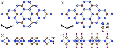
Silicene is the silicon-based counterpart of graphene with a honeycomb-like structure, which exhibits significant potential industrial applications. In the theoretical design of silicene, we have recently proposed SL h10-Si that can be exfoliated from the bulk allotrope.33 SL h10-Si exhibits a honeycomb-like structure isostructural to the 2 × 2 large honeycomb dumbbell silicene (LHDS) in Cahangirov's work.13 It is worth noting that similar dumbbell-like features can be observed in previous experiments,11,12 indicating that SL h10-Si is experimentally achievable.For pristine SL h10-Si, Si1 atoms are located in the a–b plane, while Si2 atoms are connected to form the large honeycomb dumbbell structure, as shown in Fig. 1(a). For fully hydrogenated SL h10-Si as shown in Fig. 1(b), the hydrogen atoms are attached to Si2 atoms through the Si2–H bonds with the bond lengths of 1.501 Å, which subsequently forms a large-honeycomb structure. To clearly understand the hydrogenation effects on the structure of SL h10-Si, we compare the lattice parameter, a, and the thickness of the silicon layer, d, of SL h10-Si and bulk h10-Si, as shown in Table 1. It is found that, after hydrogenation, d is increased from 2.712 Å to 2.831 Å, while a is reduced from 7.428 Å to 7.380 Å. This means that hydrogenation induces an equivalent uniaxial tensile strain, εd, of 4.4%, which is obviously lower than that (7.1%) in 10.5% stretched bulk h10-Si. Here, εd is defined as the change rate of d, which is different from the conventional uniaxial tensile strain defined by the change rate of the c-axis.33 In SL h10-Si, εd leads to a biaxial compressive strain, εxy, of −0.6% on the a–b plane. The produced εxy is close to that induced by a c-axis uniaxial tensile strain of about 10.5% in bulk h10-Si, which triggers the electronic transition from an indirect to a direct band gap in bulk h10-Si. Therefore, we take SL h10-Si as an example to explore the hydrogenation-induced strain effects on the electronic properties of similar 2D materials.
| Structure | d (Å) | ε d (%) | a (Å) | ε xy (%) |
|---|---|---|---|---|
| Pristine SL h10-Si | 2.712 | 7.428 | ||
| Fully hydrogenated SL h10-Si | 2.831 | 4.4 | 7.380 | −0.6 |
| Pristine bulk h10-Si | 2.887 | 7.366 | ||
| 10.5% stretched bulk h10-Si | 3.092 | 7.1 | 7.320 | −0.6 |
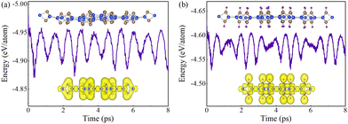
We first carry out the AIMD simulations and the phonon spectra calculations to discuss the thermal and dynamical stabilities of pristine and fully hydrogenated SL h10-Si. The energy fluctuations of pristine and fully hydrogenated SL h10-Si as a function of the simulated time are shown in Fig. 2, in which the snapshots of the above two structures at 8 ps and the corresponding ELF are inserted. Clearly, there is no tendency of decomposition up to 400 K both in pristine and fully hydrogenated SL h10-Si, indicating their thermal stabilities. In particular, the degree of structural distortion for fully hydrogenated SL h10-Si is significantly weakened, indicating the hydrogenation-enhanced thermal stability in SL h10-Si. We attribute this enhancement to the formation of the all-sp3 silicon skeleton and strong covalent interaction between silicon and hydrogen atoms, which can be proved by the ELF shown in the bottom insets of Fig. 2. Additionally, the calculated phonon spectra of pristine and fully hydrogenated SL h10-Si are shown in Fig. S1 (ESI†). The absence of the imaginary frequency throughout the Brillouin zone (BZ) signals their dynamical stabilities. Therefore, it is reasonable to explore the electronic transition in SL h10-Si during the hydrogenation process.
3.2. Electronic properties
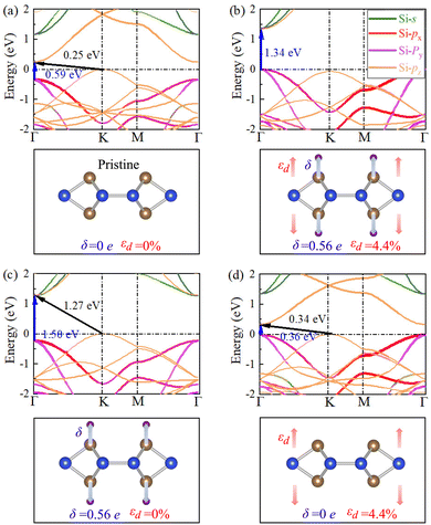
The electrons in pristine SL h10-Si are confined in 2D silicon atomic sheets, which may lead to novel electronic structures and physical properties different from the bulk case. To understand the electronic properties, the orbital-projected electronic band structure of pristine SL h10-Si is calculated and shown in Fig. 3(a). It clearly shows the semiconducting features of pristine SL h10-Si with an indirect band gap of 0.25 eV, where the valence band maximum (VBM) and conduction band minimum (CBM) are located at the K (−1/3, 2/3, 0) and Γ (0, 0, 0) points, respectively. From the band structure, it is found that the VBM mostly comes from the pz orbitals and the valence band submaximum mainly comes from the px and py orbitals, while the CBM mainly originates from the pz orbital. Compared with bulk h10-Si,33 the composition of the electronic contribution for the band edges of pristine SL h10-Si almost remains the same. The only difference comes from the CBM, where the CBM of pristine SL h10-Si is contributed mainly by the pz orbital while that of bulk h10-Si is contributed mainly by s/pz hybrid orbitals. This means that, like bulk h10-Si, the electronic structure of SL h10-Si can be significantly tuned by anisotropic strain such as hydrogenation-induced equivalent strain. The orbital-projected electronic band structure of fully hydrogenated SL h10-Si is also calculated and shown in Fig. 3(b). It can be clearly found that fully hydrogenated SL h10-Si is a direct-band-gap semiconductor with a band gap of 1.34 eV, which is defined as the energy difference between VBM and CBM both at the Γ point.For conduction bands, two unoccupied pz bands are occupied by hydrogen states, which directly leads to a significant increase in the band gap. As shown in Fig. S2 (ESI†), the hydrogen states are mainly distributed in the deep energy levels. In other words, hydrogen states mainly change the features of the conduction bands of SL h10-Si during the hydrogenation process. To consider the influence of hydrogenation-induced charge transfer, we calculate the orbital-projected electronic band structures of the pristine structure after hydrogen atoms are attached and perform Bader analysis of fully hydrogenated SL h10-Si, as shown in Fig. 3(c) and Table S1 (ESI†). These results also prove that the hydrogenation-induced charge transfer mainly influences the features of the conduction bands.
For the valence bands, we calculate the orbital-projected electronic band structures of the fully hydrogenated structure after hydrogen atom removal, as shown in Fig. 3(d). In Fig. 3(d), the hydrogenation effect is equivalent to the uniaxial tensile strain effect. Under the equivalent strain, the px/py bands move toward the Fermi level with respect to the pz band. This is due to the fact that the equivalent strain can weaken the interactions between pz orbitals and simultaneously enhance those between px and py orbitals.33,42 The enhanced interactions of px and py orbitals can further strengthen the Coulomb repulsion, leading to the px/py bands shifting up in the energy. In the above case, the synergistic effect of hydrogenation-induced charge transfer and equivalent strain leads to an electronic transition from an indirect to a direct band gap in SL h10-Si. It needs to be emphasized that hydrogenation-induced equivalent strain plays a predominant role in the electronic transition because the shift amplitude of the band edge caused by the equivalent strain is significantly larger than that caused by charge transfers. We also performed HSE06 calculations to check our PBE results, as shown in Fig. S3 (ESI†). In general, the calculated HSE06 band gaps for different cases are larger than those at the PBE level, but the qualitative features of the energy bands are changed little. Therefore, the choice of the exchange–correlation functional does not affect the conclusion that hydrogenation-induced equivalent strain plays a dominant role in tuning the physical properties of the hydrogenated materials.
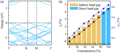
Next, considering that the ideal full hydrogenation is difficult to achieve experimentally,24,25 we further explore the partially hydrogenated cases in SL h10-Si. A 2 × 2 × 1 supercell including 40 silicon atoms is built as the basic model, and the hydrogenation concentrations are set to be 0%, 12.5%, 25.0%, 37.5%, 50.0%, 62.5%, 75.0%, 87.5%, and 100%, respectively. Here, the hydrogenation concentration is defined as the ratio of the number of hydrogen atoms to dangling bonds. For each hydrogenation concentration, all possible structures are fully relaxed and the lowest-energy structure is considered here. The evolution of the structures and corresponding phonon spectra of SL h10-Si during the hydrogenation process are shown in Figs. S4 and S5 (ESI†). As shown in Fig. S5 (ESI†), the acoustic branches of the phonon spectra of partially hydrogenated SL h10-Si have tiny soft-modes, which may appear due to the numerical differences and are not a sign of instability.43,44Fig. 4(a) and Fig. S6 (ESI†) show the hydrogenation-induced evolution of the electronic band structures. The CBM rigidly locates at the Γ point, while the VBM shifts from the K to Γ point at the hydrogenation concentration of about 87.5%. This means that SL h10-Si transforms to a direct-band-gap semiconductor at the hydrogenation concentration of about 87.5%. The band gaps, εd, and εxy of SL h10-Si for different hydrogenation concentrations are shown in Fig. 4(b). It is found that the band gaps, εd, and εxy linearly climb up with the increase of the hydrogenation concentration. The almost synchronous trend of the band gaps and equivalent strain also roughly confirms the dominant influence of equivalent strain on the electronic structures of SL h10-Si.
Note that hydrogenation has been widely used to tune the physical properties of 2D materials both in theory and experiments.45,46 However, the hydrogenation-induced strain effects on the electronic properties of 2D materials have not attracted much attention due to the tiny lattice distortion. The electronic transition in the hydrogenated SL h10-Si in our work proves the importance of equivalent strain effects in the hydrogenation process, which deserves attention in the research of 2D materials.
3.3. Optical properties
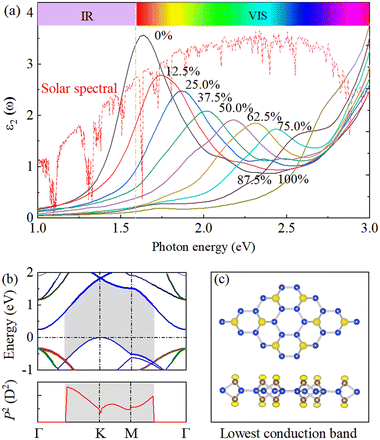
Finally, we discuss the optical properties of SL h10-Si that are directly related to its electronic structure. We explore the light absorption spectrum of SL h10-Si by calculating the imaginary part of the dielectric function (ε2) compared with the reference air mass (AM) 1.5 solar spectral irradiance, as shown in Fig. 5(a). Similar to its electronic properties, ε2 of SL h10-Si exhibits a strong hydrogenation-concentration dependence. It can be clearly found that with the increase of the hydrogenation concentration, the visible (VIS) light absorption peak continuously shifts from 1.64 to 2.44 eV in the concentration range of 0–75.0%, where solar spectral irradiation has its maximum intensity. Therefore, in addition to uniaxial tensile strain, hydrogenation-induced equivalent strain can also continuously tune the light absorption spectrum in a wide range of 0.80 eV. Interestingly, the magnitude of the total shift is comparable to that in strain-tuned silicon33 and black phosphorus,47 but is larger than that in doped Si–Ge alloy.48 On the other hand, with the hydrogenation concentration beyond 87.5%, the intensity of the VIS absorption peak is blunted. This indicates that a direct band gap does not arbitrarily mean better light absorption performance than the indirect one.The transition probabilities between the top valence and the lowest conduction bands directly relate to the sum of the squares of the dipole transition matrix elements, P2, in BZ.49,50 Therefore, to understand the physical mechanism behind the modification of the light absorption spectrum of SL h10-Si, we calculate the P2 values to discuss the transition probabilities, as shown in Fig. 5(b) and Fig. S7 (ESI†). One can easily conclude that the pz–pz dipole transition dominates the light absorption performance while the px/py–pz dipole transitions are forbidden. The almost parallel bands originating from the unoccupied and occupied pz orbitals, with the energy gaps in the range of 1.52–2.02 eV, lead to the VIS absorption peak of pristine SL h10-Si. Besides, the unoccupied pz orbitals mainly come from the structual edges of SL h10-Si, which are gradually occupied during the hydrogenation process, as shown in Fig. 5(c). Therefore, with the increase of the hydrogenation concentration, the position of the light absorption peak gradually blueshifts and the intensity of that slowly weakens due to the pz–pz -band-gap rises and the hydrogen occupations, respectively.
Strains have been extensively exploited to tune the optical properties of materials including bulk33,51 and 2D52,53 materials. Not surprisingly, the hydrogenation-induced absorption modification in SL h10-Si may facilitate its application in optoelectronic devices.
4. Conclusion
In conclusion, taking SL h10-Si as an example, we explore the hydrogenation-induced strain effects on the structural and physical properties of 2D materials. In this case, hydrogenation can enhance the thermal stability of SL h10-Si by strong Si–H covalent interactions. Besides, hydrogenation can trigger a direct band gap of about 1.34 eV mainly due to the hydrogenation-induced equivalent strain. Interestingly, the band gaps of SL h10-Si exhibit a strong hydrogenation-concentration dependence and an electronic transition occurs at a hydrogenation concentration of about 87.5%. The hydrogenation can also shift the light absorption peak of SL h10-Si in the photon-energy range of 1.64–2.44 eV. Our results not only provide an example of stabilizing the free-standing structure and tuning the physical properties of SL h10-Si, but also provide a universal understanding of hydrogenation-induced equivalent strain effects in similar 2D materials.Conflicts of interest
There are no conflicts to declare.Acknowledgements
We acknowledge support from the National Natural Science Foundation of China (Grants No. 12074153, 11674131, and 12204202), the Natural Science Foundation of Jiangsu Province (Grant No. BK20220679), the Natural Science Fund for Colleges and Universities in Jiangsu Province (Grant No. 22KJB140010), and Jiangsu Normal University (Grant No. 21XSRS006).References
- A. K. Geim, Science, 2009, 324, 1530, DOI:10.1126/science.1158877.
- Y.-L. Li, E. Stavrou, Q. Zhu, S. M. Clarke, Y. G. Li and H.-M. Huang, Nanoscale, 2019, 99(22), 220503, DOI:10.1103/PhysRevB.99.220503.
- X. Zhang and Y. Xie, Chem. Soc. Rev., 2013, 42, 8187, 10.1039/C3CS60138B.
- P. Jiang, L. L. Kang, Y.-L. Li, X. H. Zheng, Z. Zeng and S. Sanvito, Phys. Rev. B, 2021, 104(3), 035430, DOI:10.1103/PhysRevB.104.035430.
- T. H. Osborn, A. A. Farajian, O. V. Pupysheva, R. S. Aga and L. L. Y. Voon, Chem. Phys. Lett., 2011, 511, 101, DOI:10.1016/j.cplett.2011.06.009.
- M. A. Kharadi, G. F. A. Malik, F. A. Khanday, K. A. Shah, S. Mittal and B. K. Kaushik, ECS J. Solid State Sci. Technol., 2020, 9, 115031, DOI:10.1149/2162-8777/abd09a.
- J. Zhuang, X. Xu, H. Feng, Z. Li, X. Wang and Y. Du, Sci. Bull., 2015, 60, 1551, DOI:10.1007/s11434-015-0880-2.
- S. Cahangirov, M. Topsakal, E. Aktürk, H. Sahin and S. Ciraci, Phys. Rev. Lett., 2009, 102, 236804, DOI:10.1103/PhysRevLett.102.236804.
- C.-C. Liu, W. Feng and Y. Yao, Phys. Rev. Lett., 2011, 107, 076802, DOI:10.1103/PhysRevLett.107.076802.
- L. Chen, C.-C. Liu, B. Feng, X. He, P. Cheng, Z. Ding, S. Meng, Y. Yao and K. Wu, Phys. Rev. Lett., 2012, 109, 056804, DOI:10.1103/PhysRevLett.109.056804.
- L. Chen, H. Li, B. Feng, Z. Ding, J. Qiu, P. Cheng, K. Wu and S. Meng, Phys. Rev. Lett., 2013, 110, 085504, DOI:10.1103/PhysRevLett.110.085504.
- B. Feng, Z. Ding, S. Meng, Y. Yao, X. He, P. Cheng, L. Chen and K. Wu, Nano Lett., 2012, 12, 3507, DOI:10.1021/nl301047g.
- S. Cahangirov, V. O. Özçelik, L. Xian, J. Avila, S. Cho, M. C. Asensio, S. Ciraci and A. Rubio, Phys. Rev. B: Condens. Matter Mater. Phys., 2014, 90, 035448, DOI:10.1103/PhysRevB.90.035448.
- X. Zheng, L. Huang, X. Wang, J. Lan and Z. Zeng, Comput. Mater. Sci., 2012, 62, 93, DOI:10.1016/j.commatsci.2012.05.022.
- Y. F. Li, G. H. Tang and B. Fu, Phys. Rev. B, 2019, 99, 235428, DOI:10.1103/PhysRevB.99.235428.
- E. Cadelano, P. L. Palla, S. Giordano and L. Colombo, Phys. Rev. B: Condens. Matter Mater. Phys., 2010, 82, 235414, DOI:10.1103/PhysRevB.82.235414.
- P. Manchanda, A. Enders, D. J. Sellmyer and R. Skomski, Phys. Rev. B, 2016, 94, 104426, DOI:10.1103/PhysRevB.94.104426.
- J. Bekaert, M. Petrov, A. Aperis, P. M. Oppeneer and M. V. Milosevic, Phys. Rev. Lett., 2019, 123, 077001, DOI:10.1103/PhysRevLett.123.077001.
- P. Zhang, X. Li, C. Hu, S. Wu and Z. Zhu, Phys. Lett. A, 2012, 376, 1230, DOI:10.1016/j.physleta.2012.02.030.
- Z. Liu, X. Wu and T. Luo, 2D Mater., 2017, 4, 025002, DOI:10.1088/2053-1583/aa533e.
- C.-W. Zhang and S.-S. Yan, J. Phys. Chem. C, 2012, 116, 4163, DOI:10.1021/jp2104177.
- P. Jiang, L. Kang, X. Tao, N. Cao, H. Hao, X. Zheng, L. Zhang and Z. Zeng, J. Phys.: Condens. Matter, 2019, 31, 495701, DOI:10.1088/1361-648x/ab3dd6.
- H. Chen, P. Yan, J. Li, C. He, T. Ouyang, C. Zhang, C. Tang and J. Zhong, J. Appl. Phys., 2020, 127, 084301, DOI:10.1063/1.5124856.
- J. Qiu, H. Fu, Y. Xu, A. I. Oreshkin, T. Shao, H. Li, S. Meng, L. Chen and K. Wu, Phys. Rev. Lett., 2015, 114, 126101, DOI:10.1103/PhysRevLett.114.126101.
- J. Qiu, H. Fu, Y. Xu, Q. Zhou, S. Meng, H. Li, L. Chen and K. Wu, ACS Nano, 2015, 9, 11192, DOI:10.1021/acsnano.5b04722.
- Y.-J. Kim, Y. Kim, K. Novoselov and B. H. Hong, 2D Mater., 2015, 2, 042001, DOI:10.1088/2053-1583/2/4/042001.
- Y. Liao, X. Shi, T. Ouyang, J. Li, C. Zhang, C. Tang, C. He and J. Zhong, J. Phys. Chem. Lett., 2021, 12, 8889, DOI:10.1021/acs.jpclett.1c02364.
- L. Lew Yan Voon, E. Sandberg, R. Aga and A. Farajian, Appl. Phys. Lett., 2010, 97, 163114, DOI:10.1063/1.3495786.
- S. Deng, A. V. Sumant and V. Berry, Nano Today, 2018, 22, 14, DOI:10.1016/j.nantod.2018.07.001.
- S. Song, D. H. Keum, S. Cho, D. Perello, Y. Kim and Y. H. Lee, Nano Lett., 2016, 16, 188, DOI:10.1021/acs.nanolett.5b03481.
- J. Feng, X. Qian, C.-W. Huang and J. Li, Nat. Photonics, 2012, 6, 866, DOI:10.1038/nphoton.2012.285.
- G. H. Ahn, M. Amani, H. Rasool, D.-H. Lien, J. P. Mastandrea, J. W. Ager III, M. Dubey, D. C. Chrzan, A. M. Minor and A. Javey, Nat. Commun., 2017, 8, 608, DOI:10.1038/s41467-017-00516-5.
- D. Zhang, H. Niu, Y. Li, H.-M. Huang, P. Jiang and Y.-L. Li, Phys. Rev. B, 2021, 104, 125201, DOI:10.1103/PhysRevB.104.125201.
- J. Hafner, Comput. Phys. Commun., 2007, 177, 6, DOI:10.1016/j.cpc.2007.02.045.
- G. Kresse and J. Furthmüller, Phys. Rev. B: Condens. Matter Mater. Phys., 1996, 54, 11169, DOI:10.1103/PhysRevB.54.11169.
- N. Holzwarth, A. Tackett and G. Matthews, Comput. Phys. Commun., 2001, 135, 329, DOI:10.1016/S0010-4655(00)00244-7.
- J. P. Perdew, K. Burke and M. Ernzerhof, Phys. Rev. Lett., 1996, 77, 3865, DOI:10.1103/PhysRevLett.77.3865.
- K. Parlinski, Z. Q. Li and Y. Kawazoe, Phys. Rev. Lett., 1997, 78, 4063, DOI:10.1103/PhysRevLett.78.4063.
- S. Baroni, S. De Gironcoli, A. Dal Corso and P. Giannozzi, Rev. Mod. Phys., 2001, 73, 515, DOI:10.1103/RevModPhys.73.515.
- W. G. Hoover, Phys. Rev. A: At., Mol., Opt. Phys., 1985, 31, 1695, DOI:10.1103/PhysRevA.31.1695.
- J. Heyd, G. E. Scuseria and M. Ernzerhof, J. Chem. Phys., 2003, 118, 8207, DOI:10.1063/1.1564060.
- B. Ram and A. K. Singh, Phys. Rev. B, 2017, 95, 075134, DOI:10.1103/PhysRevB.95.075134.
- M. Gao, Q.-Z. Li, X.-W. Yan and J. Wang, Phys. Rev. B, 2017, 95, 024505, DOI:10.1103/PhysRevB.95.024505.
- H. Sahin, S. Cahangirov, M. Topsakal, E. Bekaroglu, E. Akturk, R. T. Senger and S. Ciraci, Phys. Rev. B: Condens. Matter Mater. Phys., 2009, 80, 155453, DOI:10.1103/PhysRevB.80.155453.
- K. Xue and Z. Xu, Appl. Phys. Lett., 2010, 96, 063103, DOI:10.1063/1.3298552.
- L. Thevenard, L. Largeau, O. Mauguin, A. Lematre and B. Theys, Appl. Phys. Lett., 2005, 87, 182506, DOI:10.1063/1.2126147.
- D. Çakir, H. Sahin and F. M. C. M. Peeters, Phys. Rev. B: Condens. Matter Mater. Phys., 2014, 90, 205421, DOI:10.1103/PhysRevB.90.205421.
- E. M. Fadaly, A. Dijkstra, J. R. Suckert, D. Ziss, M. A. van Tilburg, C. Mao, Y. Ren, V. T. van Lange, K. Korzun and S. Kölling, et al. , Nature, 2020, 580, 205, DOI:10.1038/s41586-020-2150-y.
- A. E. Maughan, A. M. Ganose, M. M. Bordelon, E. M. Miller, D. O. Scanlon and J. R. Neilson, J. Am. Chem. Soc., 2016, 138, 8453, DOI:10.1021/jacs.6b03207.
- W. Meng, X. Wang, Z. Xiao, J. Wang, D. B. Mitzi and Y. Yan, J. Phys. Chem. Lett., 2017, 8, 2999, DOI:10.1021/acs.jpclett.7b01042.
- M. El Kurdi, H. Bertin, E. Martincic, M. De Kersauson, G. Fishman, S. Sauvage, A. Bosseboeuf and P. Boucaud, Appl. Phys. Lett., 2010, 96, 041909, DOI:10.1063/1.3297883.
- B. Sa, Y.-L. Li, J. Qi, R. Ahuja and Z. Sun, J. Phys. Chem. C, 2014, 118, 26560, DOI:10.1021/jp508618t.
- Y. Li, Y.-L. Li, B. Sa and R. Ahuja, Catal. Sci. Technol., 2017, 7, 545, 10.1039/C6CY02178F.
Footnote |
| † Electronic supplementary information (ESI) available. See DOI: https://doi.org/10.1039/d2cp04855h |
| This journal is © the Owner Societies 2023 |

