
 Open Access Article
 This Open Access Article is licensed under a Creative Commons Attribution-Non Commercial 3.0 Unported Licence
In situ tuning of the performance of polymer field-effect transistors by soft plasma etching†
Zhen
Hu‡
ab,
Dongfan
Li‡
*ab,
Wanlong
Lu
ab,
Zongze
Qin
ab,
Yixin
Ran
ab,
Xin
Wang
ab and
Guanghao
Lu
 *ab
*ab
aFrontier Institute of Science and Technology, Xi’an Jiaotong University, Xi’an 710054, P. R. China
bState Key Laboratory of Electrical Insulation and Power Equipment, Xi’an Jiaotong University, Xi’an 710049, China. E-mail: dongfan.li@foxmail.com; guanghao.lu@mail.xjtu.edu.cn
First published on 22nd May 2023
Abstract
Organic semiconductor films prepared by solution methods usually produce a large number of charge traps, which significantly increase the subthreshold swing (SS) of organic field-effect transistors (OFETs) with threshold voltage (Vth) far from 0 V, making it difficult for the OFETs to operate at low voltages. In this work, we found that after soft plasma (air pressure below 15 Pa) etching, the SS of the semiconductor poly[4-(4,4-dihexadecyl-4H-cyclopenta[1,2-b:5,4-b′]-dithiophen-2-yl)- alt-[1,2,5]thiadiazolo-[3,4-c]pyridine (PCDTPT)-based OFETs reduces by approximately 60%, and Vth approaches 0 V. Meanwhile, the hysteresis of the OFETs is eliminated, indicating that soft plasma etching can improve operational stability. It was also found that the soft plasma could increase the on–off ratio by two orders of magnitude of the damaged OFETs and reduce the Vth to around 0 V. In addition, we have also demonstrated the importance and universality of the soft plasma post-treatment process in other p-type materials and heterojunction systems and have built a preliminary invertor structure based on this.
Introduction
Due to their flexibility and low cost, organic semiconductors are widely used in solar cells, organic field-effect transistors (OFETs), flexible electronics, memory devices, and sensors.1–6 However, due to the presence of traps in organic semiconductor films, the charge carriers preferentially fill the traps under gate voltage (Vgs) manipulation, resulting in threshold voltages (Vth) far away from 0 V and a high subthreshold swing (SS).7,8 A high SS with Vth far away from 0 V makes low-voltage operation of OFETs difficult and leads to overestimated or underestimated mobility.9,10 In addition, the traps, located in the semiconductor/dielectric interface or semiconductor films, result in hysteresis, resulting in OFETs with poor operational stability.11 Various approaches have been tried to reduce the SS and the Vth of OFETs with improved stability, including using high-performance organic semiconductors12,13 or doping.14–19 However, it is worth noting that these conventional methods are often expensive and difficult to use for large-scale production. Therefore, it is inspiring to seek a low-cost and simple method to improve OFETs’ performance. We have found that when the air pressure is below 20 Pa, soft plasma etches only the surface of the semiconductor film without damaging the sub-layer.20 Since charge distribution is nonuniform in the thickness direction of the organic semiconductor film,21,22 it is possible to manipulate charge distribution and optimize OFETs’ performance via layer-by-layer etching of the organic semiconductor film by controlling the soft plasma treatment time.23,24In this work, it is found that using poly[4-(4,4-dihexadecyl-4H-cyclopenta[1,2-b:5,4-b′]-dithiophen-2-yl)-alt-[1,2,5] thiadiazolo-[3,4-c]pyridine (PCDTPT) as the model polymer semiconductor, soft plasma etching can reduce the SS of the OFETs, with Vth approaching 0 V. Meanwhile, soft plasma etching can also improve OFETs’ operational stability, without damaging mobility and the on–off ratio. It was also found that the damaged OFETs with a poor on–off ratio and high Vth can be improved by using soft plasma etching. As a result, the on–off ratio increases by two orders of magnitude, and the Vth decreases from 40 V to 0 V. In addition, in situ soft plasma etching can also be applied to other polymer semiconductors such as poly[(4,4,9,9-tetrahexadecyl-4,9-dihydro-s-indaceno[1,2-b:5,6-b′]dithiophene-2,7-diyl)-alt-(benzo[c][1,2,5]thiadiazole-4,7-diyl) (IDT-BT), poly[2,5-(2-octyldodecyl)-3,6-diketopyrrolopyrrole-alt-5,5-(2,5-di(thien-2-yl)thieno [3,2-b]thiophene)] (DPP-DTT), and PCDTPT/Polystyrene (PS) blend films. Compared to ultra-thin semiconductor film transistors, the use of soft plasma allows in situ etching of semiconductor films, and reduces material processing to tune OFETs’ performance.
Results and discussion
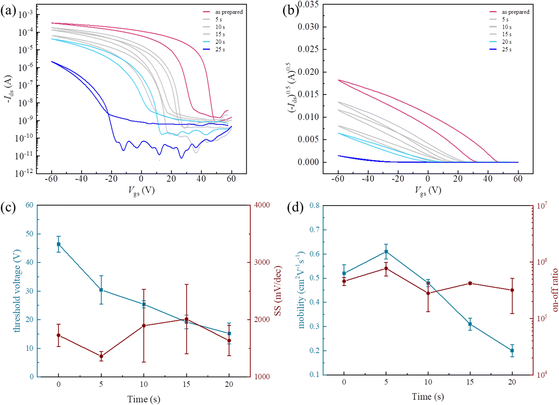
Devices with a bottom-gate-bottom-contact device structure were prepared by pre-depositing gold electrodes on clean Si/SiO2 wafers modified by OTS treatment, followed by treating them in an atmosphere of pentafluorothiophenol at 90 °C for 40 min and spin-coating a layer of PCDTPT film (Fig. 1), which were placed on a heating table for a period of annealing and then tested for electrical properties at room temperature. The PCDTPT films on the device surface were etched using air plasma for 5 s at a time to test the change in electrical properties. The effects of air plasma etching on organic semiconductor films and devices were observed. The process of soft plasma etching of organic semiconductor films is shown in Fig. 1. There are various ways of generating plasma; our focus is on glow discharge plasma technology, and based on this we hope to achieve various properties of the organic field effect transistor devices by subsequent processing of the devices through glow discharge plasma etching. When we apply a very high voltage to the two ends of a low-pressure gas and break down the gas, some of the gas molecules are ionized to form anions and cations. The potential difference between the two ends of the gas generates an electric field, causing the anions and cations to move towards the positively and negatively charged ends of the gas. In the movement, they collide with other gas molecules, ionizing them and eventually creating plasma between the electrode plates. During this process, different gases emit different colored glows, which is the so-called “glow discharge”. When we put the OFETs between the electrode plates, the soft plasma collide on the surface of the semiconductor layer of the OFETs and eventually the etching process is achieved. The transfer curve of the device before and after soft plasma etchings is presented in Fig. 2a and b, respectively. As can be observed from the graph, the transfer curve shifts gradually to the left as the etching time increases. The specific trend of Vth is illustrated in Fig. 2c. The Vth of the devices based on bottom–gate-bottom-contact structures is approximately 50 V, and the curve displays considerable hysteresis, indicating the difficulty in low-voltage operation. However, after 5 and 10 seconds of air plasma etching, Vth reduces to around 0 V. The hysteresis of the transfer curves is also reduced, and the curves nearly coincide, implying that Vth has been effectively reduced after soft plasma treatment and the treated devices can be used in low-voltage operation. On the basis of Fig. 2a we have calculated the SS of the device using the following equation: | (1) |
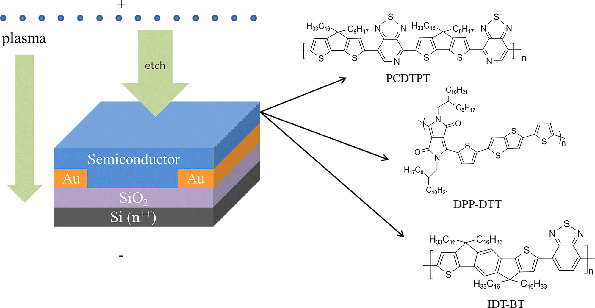 | ||
| Fig. 1 Structure of OFETs with a bottom-gate-bottom-contact configuration and the process of soft plasma etching of the semiconductor layer. The polymer semiconductor layer studied in this work is PCDTPT, DPP-DTT, or IDT-BT. Soft plasma incrementally etches the polymer layer from the top side, without causing damage to the polymer materials underneath the etched surface, which warrants the charge transport near the semiconductor/dielectric interface. | ||
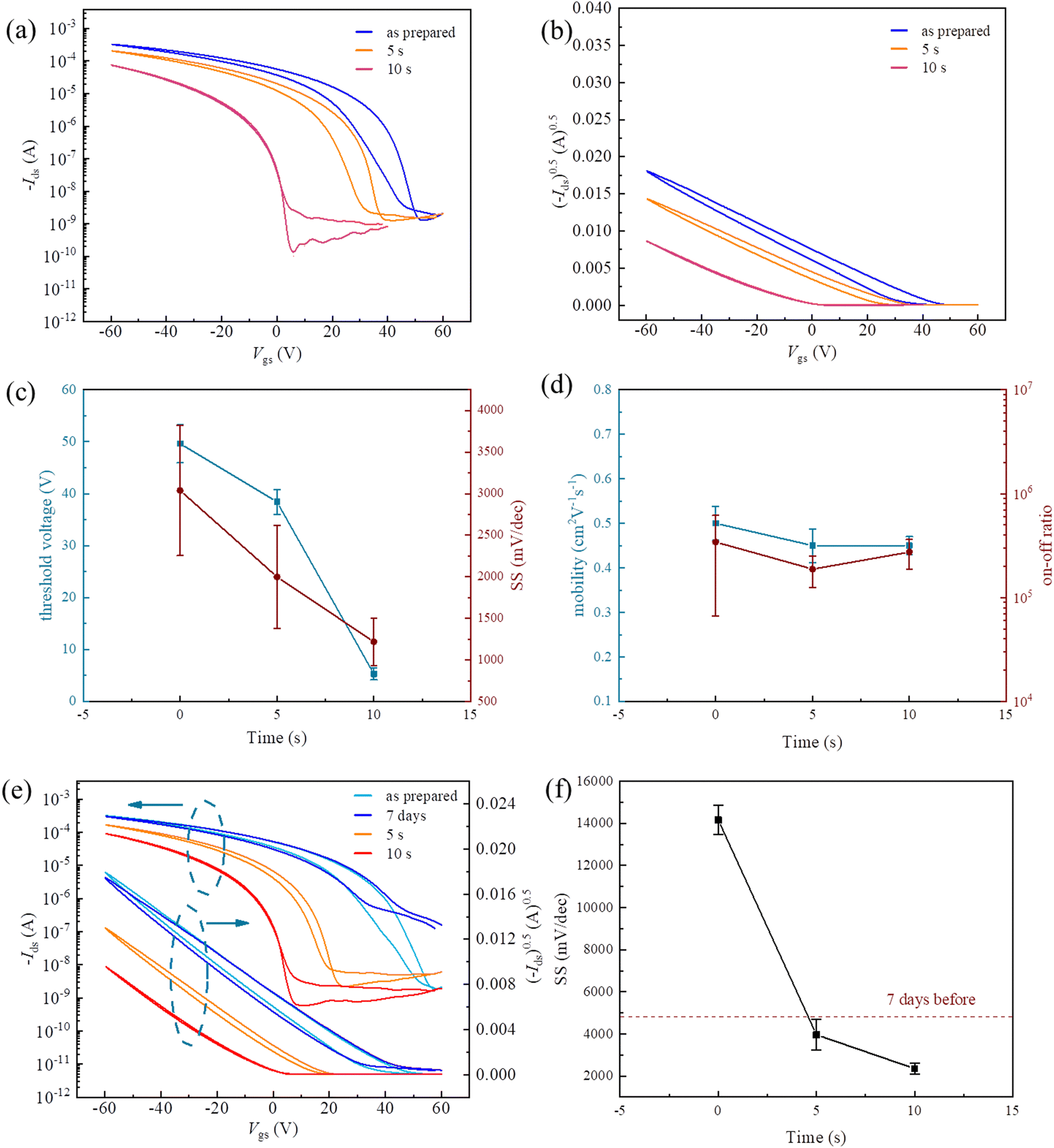 | ||
| Fig. 2 Performance of OFETs prepared by PCDTPT (a) Transfer curve of the device after plasma etching treatment. (b) Transfer curve ((−Ids1/2–Vgs)) of the device after plasma etching treatment. (c) Changes in Vth and SS of the device after plasma treatment. (d) Changes in mobility and the on–off ratio of the device after plasma treatment. (e) Plasma-etched transfer curve of a device after 7 days in the air. (f) SS of the device after plasma etching treatment (the device was left in air for some time before treatment). | ||
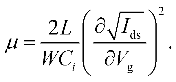
In the above equation Ids means the source-drain current. As shown in Fig. 2c, the SS of the device decreases significantly with increasing etching time, which means that air plasma etching can increase the speed of switching from the off to on state. The mobility of the OFETs is always the most important characteristic of an electronic device and its value is largely indicative of the performance of the device, so we have also calculated the effect of plasma etching on the mobility of the device and finally got the images of the mobility of the device as a function of etching time based on the following equation:
 | (2) |
In the above equation L is the channel length of the device, W is the channel width of the device and Ci is the capacitance per unit area of the insulating layer in the device. Finally, as shown in Fig. 2d, we have calculated the trend of the mobility of the device and the on–off ratio with etching time. As can be seen from the graph, these two parameters do not change significantly over a range of etching times.
The untreated device experiences a significant drop in the on–off ratio after 7 days in the air, leading to the loss of current-regulating ability (Fig. 2e). This issue can be solved by applying soft plasma etching for 5–10 seconds, which results in the reduction of Vth to around 0 V, eliminating the hysteresis, and substantially improving the on–off ratio by 2 orders of magnitude. Therefore, when organic field-effect transistors are over doped, soft plasma etching can restore device performance. Fig. 2f also indicates that the SS is much higher after exposure of the devices for 7 days in the air, of which the SS can be effectively reduced by soft plasma etching. We subsequently compared the air stability difference between OFET devices fabricated using PCDTPT, with and without 25 seconds of soft plasma etching treatment (Fig. S1, ESI†). After comparing the results, we found that prolonged soft plasma etching treatment does not improve the air stability of the device. After being left in air for a certain period of time, the transfer curves of the device would shift towards the positive direction.
By applying soft plasma etching treatment to devices composed of various other organic semiconductor materials, we observed analogous phenomena.
Fig. 3a demonstrates that after spin-coating an IDT-BT organic semiconductor film onto a treated gold electrode, a bottom–gate-bottom-contact device with the same structure was produced and layer-by-layer soft plasma etching was performed to obtain the transfer curve trend of the device. Fig. 3b shows that the device became highly sensitive to soft plasma etching. The Vth reduces to approximately 0 V during 5 and 10 seconds of air plasma etching, and the hysteresis decreases dramatically. Similarly, we observed a comparable phenomenon as we calculated the change in the device's SS, as shown in Fig. 3b. The SS of the device gradually decreased during soft etching. Fig. 3c illustrates that the trend of mobility and on–off ratio of the device remains unchanged by soft plasma etching. The output curve of the IDT-BT transistor is depicted in Fig. 3d, revealing a slight reduction in Ids after soft plasma etching treatment for 5 seconds. We also compared the air stability difference between OFET devices fabricated using IDT-BT, with and without 30 seconds of soft plasma etching treatment (Fig. S2, ESI†). From the graph we found that prolonged etching of soft plasma does not have a significant impact on the air stability of the device, as the transfer curve of the device remains largely unchanged after being left in the air for a period of time.
 | ||
| Fig. 3 Performance of OFETs prepared by IDT-BT (a) transfer curve of the device after plasma etching treatment. (b) Changes in Vth and SS of the device after plasma treatment. (c) Changes in mobility and the on–off ratio of the device after plasma treatment. (d) Output curve of the device (prepared by IDT-BT) before and after plasma etching treatment for 5 s. | ||
Fig. 4a–c demonstrate that the untreated DPP-DTT-based device shows a high Vth, huge hysteresis. By using soft plasma etching, the Vth approaches 0 V. At 25 seconds, the transfer curve is degraded significantly, suggesting that the thin DPP-DTT film may have been damaged by soft plasma etching. Fig. 4c shows that plasma etching had little impact on SS. Fig. 4d shows the on–off ratio remained relatively constant during soft plasma etching. However, the mobility of the device initially remained stable, indicating that within 10 seconds of soft plasma etching treatment, other significant electrical properties of the device have not been significantly affected. Then we compared the air stability difference between OFET devices fabricated using DPP-DTT, with and without 20 seconds of soft plasma etching treatment (Fig. S3, ESI†). After being left in air for a certain period of time, the transfer curves of the device would shift towards the positive direction, which shows that the air stability cannot be improved by soft plasma etching treatment.
 | ||
| Fig. 4 Performance of OFETs prepared by DPP-DTT (a) transfer curve of the device after plasma etching treatment. (b) Transfer curve ((−Ids1/2–Vgs)) of the device after plasma etching treatment. (c) Changes in Vth and SS of the device after plasma treatment. (d) Changes in mobility and the on–off ratio of the device after plasma treatment. | ||
The blend system was also treated by soft plasma etching. Initially, PCDTPT and PS blend solutions were spin-coated on a treated gold electrode (at a ratio of 1![[thin space (1/6-em)]](https://www.rsc.org/images/entities/char_2009.gif) :9). Then, a bottom-gate-bottom-contact device was fabricated. The device was treated by layer-by-layer soft plasma etching. We measured the change in the transfer curve of the device, illustrated in Fig. 5a and b. The transfer curve of the PCDTPT and PS blend systems showed a similar pattern when subjected to plasma etching, as depicted in Fig. 5c. The Vth of the device was gradually shifted towards 0 V with the increase of etching time and eventually decreased to around 7.2 V. The Vth variation from the transfer curve is similar to that of the pure component PCDTPT. In Fig. 5c, the SS of the device decreases more significantly with increasing etching time, suggesting that the rate of transition from the off state to the on state is largely improved. Fig. 5d shows that the mobility and on–off ratio of the device remained stable during the etching time of 0–10 s. The air stability difference between OFET devices fabricated using blend solution (PCDTPT:PS = 1:9), with and without 30 seconds of soft plasma etching treatment was also compared (Fig. S4, ESI†). The graph also shows that the air stability of the device cannot be improved by soft plasma etching treatment.
:9). Then, a bottom-gate-bottom-contact device was fabricated. The device was treated by layer-by-layer soft plasma etching. We measured the change in the transfer curve of the device, illustrated in Fig. 5a and b. The transfer curve of the PCDTPT and PS blend systems showed a similar pattern when subjected to plasma etching, as depicted in Fig. 5c. The Vth of the device was gradually shifted towards 0 V with the increase of etching time and eventually decreased to around 7.2 V. The Vth variation from the transfer curve is similar to that of the pure component PCDTPT. In Fig. 5c, the SS of the device decreases more significantly with increasing etching time, suggesting that the rate of transition from the off state to the on state is largely improved. Fig. 5d shows that the mobility and on–off ratio of the device remained stable during the etching time of 0–10 s. The air stability difference between OFET devices fabricated using blend solution (PCDTPT:PS = 1:9), with and without 30 seconds of soft plasma etching treatment was also compared (Fig. S4, ESI†). The graph also shows that the air stability of the device cannot be improved by soft plasma etching treatment.
 | ||
| Fig. 5 Performance of OFETs prepared by material mixed with PCDTPT and PS. (a) Transfer curve of the device after plasma etching treatment. (b) Transfer curve ((−Ids1/2–Vgs)) of the device after plasma etching treatment. (c) Changes in Vth and SS of the device after plasma treatment. (d) Changes in mobility and the on–off ratio of the device after plasma treatment. | ||
According to Fig. 2–5, the impact of soft plasma etching on the mobility of the device decreases at shorter etching times. While the Vth of the device varies significantly between 0 and 10 seconds of etching time, the variation is less apparent between 10 and 15 seconds. However, for materials such as DPP-DTT, the mobility of the device decreases substantially as the organic semiconductor film is etched deeper after 15 seconds of etching time. In addition, the on–off ratio, a measure of the device's ability to regulate current and a reflection of the transistor's functionality, is crucial. Fig. 2–5 show that the on–off ratios of the devices remain relatively stable during plasma etching of the organic semiconductor films, ranging between 105 and 106 orders of magnitude. Combining the previous images of the Vth of the various materials and systems, we can deduce that the Vth of these devices decreases significantly within 15 seconds of the plasma etching time, while other vital electrical properties such as mobility and on–off ratios are less impacted by plasma etching during this period. Consequently, we can conclude that an etching time of 10–15 seconds is more suitable for these materials and organic semiconductor films in this system.
Fig. 6 displays the atomic force microscopy height maps of the unetched and etched (10 s) organic semiconductor films, both of which show low roughness. These films are still homogeneous after being etched.
 | ||
| Fig. 6 (a) AFM height images of unetched and etched DPP-DTT films. (b) AFM height images of unetched and etched PCDTPT films. (c) AFM height images of unetched and etched IDT-BT films. (d) AFM height images of unetched and etched films prepared by material mixed with PCDTPT and PS (“Rrms” means RMS roughness). | ||
The in situ soft plasma etching absorbance spectra of DPP-DTT and IDT-BT organic semiconductor films (Fig. 7) show no new characteristic peaks, indicating that no other new components were produced in the films during the etching process.
 | ||
| Fig. 7 The in situ soft plasma etching absorbance spectra of DPP-DTT and IDT-BT organic semiconductor films. | ||
Fig. 8a displays the change in the linear zone transfer curve of an DPP-DTT-based OFET with a bottom–gate-bottom-contact structure after soft plasma etching with a source-drain voltage (Vds) of −10 V. The figure shows that the Vth of the device reduces to around 0 V after 14 seconds of soft plasma etching, indicating that the device is better suited for the required low-voltage operation after plasma treatment. We also applied plasma etching to an inverter circuit structure, as shown in Fig. 8b. Using the same type of OFETs, we combined a plasma-etching treated transistor with a non-plasma-etching treated transistor. When the VDD is −1 V, the output voltage–input voltage curve shown in Fig. 8b is obtained. We can see that the output voltage of this structure initially inverts the input signal by rising to nearly 1 V for a short time.
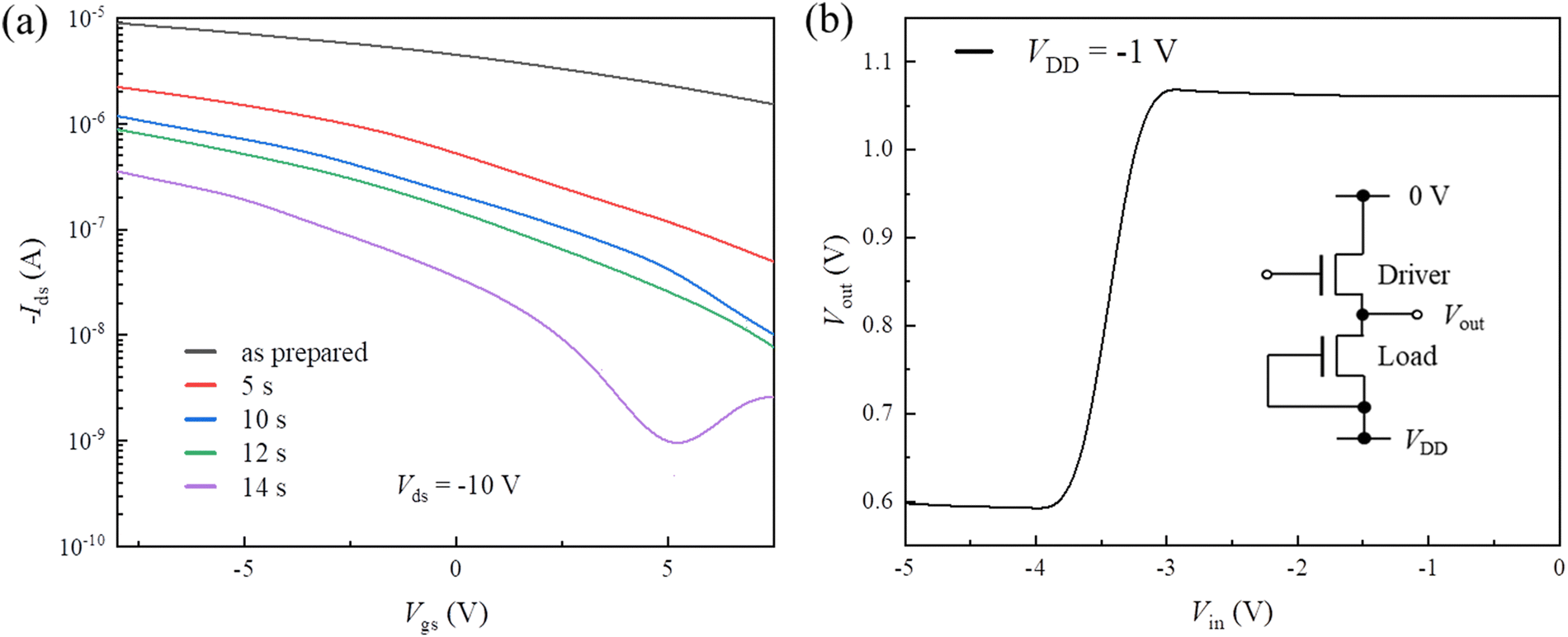 | ||
| Fig. 8 Applications of soft plasma etching of polymer thin films for low-voltage devices and digital circuits. (a) Transfer curve of the device (prepared by DPP-DTT) during plasma etching treatment, showing that the working voltage could be effectively reduced by soft plasma etching. (b) The curve of the output voltage of an inverter as a function of the input voltage (The device used in the inverter is two bottom-gate-bottom-contact transistors prepared from the PCDTPT material). | ||
In order to investigate the impact of soft plasma etching treatment on the trap density in organic semiconductor films, we used the following equation to calculate the trends of trap density for spin-coated films of PCDTPT, IDT-BT, DPP-DTT, and a blend of PCDTPT and PS (1:9) before and after soft plasma etching treatment:
 | (3) |
In the above equation Nt is the trap density in organic semiconductor films, kB is the Boltzmann constant, T means the room temperature and Ci is the capacitance per unit area of the insulating layer in the device. As shown in Fig. 9, we have calculated the variation trend of trap density for four types of organic semiconductor films after being treated with soft plasma etching. From the figure, it can be observed that the trap density of the organic semiconductor films prepared from the four systems generally decreases with the increase of etching time within 0–10 s. This indicates that soft plasma etching can indeed reduce the trap density in the thin film.
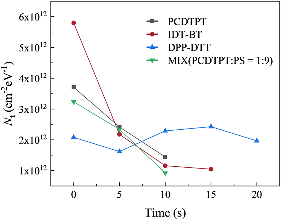 | ||
| Fig. 9 Changes in the trap density of films fabricated using four different materials after soft plasma etching. | ||
Fig. 10a illustrates that, when the gate voltage is applied in the longitudinal direction, the charge carriers in the semiconductor film are accumulated in the semiconductor layer near the dielectric layer under the action of the electric field. In practice, semiconductor films prepared by spin-coating from solutions are full of defects, resulting in trapped charges while free carriers are moving towards the thin layer under the applied voltage. After soft plasma treatment, on the one hand, the thickness of the film is reduced, and the charge carriers in the film are more likely to reach the bottom of the organic semiconductor film under the influence of Vgs. On the other hand, due to the decrease in trap density in the film after etching treatment, fewer charge carriers are trapped, and therefore, a lower Vgs is required to switch the device from the off state to the on state, resulting in a decrease in the Vth of the device. Considering the existence of oxygen in the air, we can also assume that when using air soft plasma to etch organic semiconductor films, these plasma will have a certain p-type doping effect on the films. Ultimately, this improves the charge injection process at the interface between the film and the metal electrode, thereby reducing the Vth of the device.25 In addition, because of the large number of grain boundaries in the semiconductor films, charge carriers are trapped and de-trapped according to the gate voltage sweep, thus manifesting themselves in the transfer curve as the generation of hysteresis. The soft plasma etching reduces the trap densities, resulting in fewer trapped charges, reducing the hysteresis rapidly, and causing the curves to coincide. However, when the semiconductor film is etched too thin to be discontinuous, it is difficult for carriers to conduct and the device fails to function, as shown in Fig. 10b.
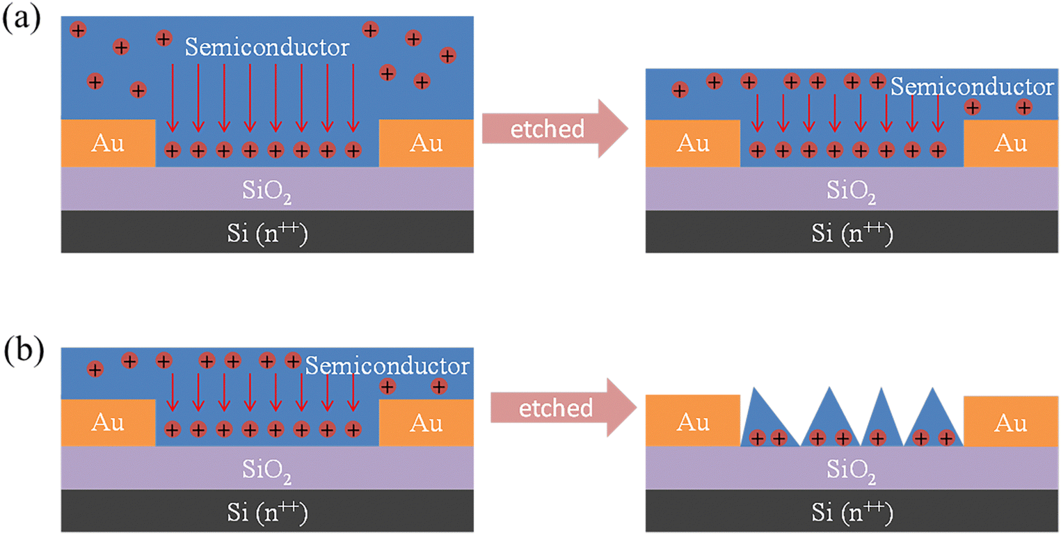 | ||
| Fig. 10 Scheme of charge distribution within the polymer semiconductor films during soft plasma etching. (a) The p-type polymers could be inevitably doped by ambient oxygen, inducing positive charges in the bulk materials and leading to the positive Vth of OFETs. After the organic semiconductor film of the device has been initially etched to a certain thickness, the carriers in the film are more likely to collect near the thin layer of the film under Vgs. (b) After the organic semiconductor film of the device has been etched too deeply, the film becomes discontinuous, making it difficult to transport carriers. | ||
Conclusions
In conclusion, soft plasma etching can effectively reduce SS with a Vth around 0 V without degrading mobility and the on–off ratio, and can be used in low voltage applications. In addition, the operational stability is improved after in situ soft plasma treatment due to the elimination of hysteresis. We have also found that soft plasma treatment has potential to improve the performance of damaged OFETs: the on–off ratio increases by two orders of magnitude and Vth reduces to around 0 V. Compared to the synthesis of high-performance organic semiconductors and dopants, in situ soft plasma has the advantage of being inexpensive, easily accessible, and simple to operate, showing broad application prospects for reducing material processing.Experimental section
Materials
PCDTPT was purchased from 1-Material Inc. DPP-DTT was purchased from Ossila. IDT-BT was purchased from Organtec Ltd. PS was purchased from Sigma-Aldrich.Device preparation
The n-type doped Si/SiO2 wafers were used and the substrates were cleaned twice in a sonicator with deionized water, acetone, and isopropanol (each time for 5 minutes) and blown dry with nitrogen gas as they went along. The substrates were then immersed in a toluene solution of OTS (OTS content of approximately 5‰) for 120 minutes at 85 °C, followed by blowing them dry again with nitrogen. Source and drain electrodes of gold material are deposited on the substrate using a mask plate at a chamber pressure of <10–4 Pa and an evaporation rate of approximately 0.6 Å s−1. The substrates containing the source and drain were then kept under an atmosphere of pentafluorothiophenol at a temperature of 90 °C for 40 minutes, after which they were removed and excess pentafluorothiophenol was gently washed off the surface of the substrates with ethanol. A chloroform solution of 8 mg ml−1 of PCDTPT (or IDT-BT, DPP-DTT) was prepared, and a mixture of 8 mg ml−1 of PCDTPT and 8 mg ml−1 of PS was chosen in a 1:9 ratio. The substrates were then spin-coated at 2000 rpm with various pure or mixed solutions. The substrates were finally annealed for one hour at a certain temperature (150 °C for PCDTPT, 100 °C for IDT-BT, and 200 °C for DPP-DTT) in a nitrogen atmosphere to finally prepare an airport effect transistor with a bottom-gate-bottom-contact structure on an n-type doped Si/SiO2 wafer.
OFETs’ characterization
The transfer curves of the OFETs were measured at room temperature and in the air using an Agilent Keysight B2900A Quick IV measurement system. The Vds of the measured saturation curves are set to −60 V and this gives the Vth of the device and the change in mobility.Air plasma treatment
A soft plasma etching process is used in the measurement of the transfer curve. For this process, the air pressure in the chamber is controlled to below 15 Pa, the air source is air and the power of the device is set to be 300 W. The same device is etched for 5 s at a time and the change in the transfer curve is subsequently measured.Conflicts of interest
The authors declare no competing financial interest.Acknowledgements
This work was supported by the National Natural Science Foundation of China (Grant No. 51873172 and 52273026) and the Key Scientific and Technological Innovation Team Project of Shaanxi Province (2021GXLH-Z-055).References
- Y. D. Zhang, X. C. Wang, F. Xian, M. M. Li, C. L. Wang and H. L. Zhang, ACS Appl. Mater. Interfaces, 2022, 14, 54885–54894 CrossRef CAS PubMed.
- P. Y. Xue, J. M. Xin, G. Y. Lu, B. Y. Jia, H. Lu, G. H. Lu, W. Ma, R. P. S. Hane and X. W. Zhan, J. Mater. Chem. C, 2023 10.1039/D2TC04507A.
- Q. Zhou, Y. Sasaki, K. Ohshiro, H. N. Fan, V. Montagna, C. Gonzato, K. Haupt and T. Minami, J. Mater. Chem. B, 2022, 10, 6808–6815 RSC.
- Y. W. Zhu, N. Qiao, S. Q. Dong, G. H. Qu, Y. Chen, W. L. Lu, Z. Z. Qin, D. F. Li, K. N. Wu, Y. J. Nie, B. Liu, S. T. Li and G. H. Lu, Chem. Mater., 2022, 34, 6505–6517 CrossRef CAS.
- T. W. Chang, Y. S. Li, N. Matsuhisabc and C. C. Shih, J. Mater. Chem. C, 2022, 10, 13372–13394 RSC.
- Y. W. Zhu, Y. K. Fan, S. T. Li, P. Wei, D. F. Li, B. Liu, D. M. Cui, Z. C. Zhang, G. C. Li, Y. J. Niee and G. H. Lu, Mater. Horiz., 2020, 7, 1861–1871 RSC.
- E. C. Plunkett, Q. Y. Zhang, H. E. Katz and D. H. Reich, ACS Appl. Electron. Mater., 2021, 3, 1656–1662 CrossRef CAS.
- F. Huang, A. Liu, H. H. Zhu, Y. Xu, F. Balestra, G. Ghibaudo, Y. Y. Noh, J. H. Chu and W. W. Li, IEEE Electron Device Lett., 2019, 40, 605–608 CAS.
- W. L. Lu, J. N. Cao, C. Y. Zhai, L. J. Bu, G. H. Lu and Y. W. Zhu, ACS Appl. Mater. Interfaces, 2022, 14, 23709–23716 CrossRef CAS PubMed.
- D. F. Li, S. T. Li, W. L. Lu, S. Feng, P. Wei, Y. P. Hu, X. Wang and G. H. Lu, IEEE J. Electron Devices Soc., 2019, 7, 303–308 CAS.
- D. F. Li, Y. W. Zhu, P. Wei, W. L. Lu, S. T. Li, S. Wang, B. Xu and G. H. Lu, IEEE Electron Device Lett., 2020, 41, 1665–1668 CAS.
- R. Dheepika, R. Abhijnakrishna, P. M. Imranb and S. Nagarajan, RSC Adv., 2020, 10, 13043–13049 RSC.
- M. N. Khatun, A. Dey, N. Meher and P. K. Iyer, ACS Appl. Electron. Mater., 2021, 3, 3575–3587 CrossRef CAS.
- P. Y. Chen, D. Y. Wang, L. Luo, J. Q. Meng, Z. Q. Zhou, X. J. Dai, Y. Zou, L. X. Tan, X. F. Shao, C. A. Di, C. Y. Jia, H. L. Zhang and Z. T. Liu, Adv. Mater., 2023, 35, 2300240 CrossRef CAS PubMed.
- M. Park, C. M. Kang, S. Park, H. Jo and J. Roh, ACS Omega, 2021, 6, 33639–33644 CrossRef CAS PubMed.
- Y. Xu, H. Sun, A. Liu, H. H. Zhu, W. W. Li, Y. F. Lin and Y. Y. Noh, Adv. Mater., 2018, 30, 1801830 CrossRef PubMed.
- J. H. Li, A. Babuji, L. Fijahi, A. M. James, R. Resel, T. Salzillo, R. Pfattner, C. Ocal, E. Barrena and M. Mas-Torrent, ACS Appl. Mater. Interfaces, 2023, 15, 5521–5528 CrossRef CAS PubMed.
- A. Łuczak, W. Waliszewski, K. Jerczynski, A. Wypych-Puszkarz, J. Rogowski, J. Pietrasik, M. Kozanecki, J. Ulanski and K. Matyjaszewski, J. Mater. Chem. C, 2022, 10, 15541–15553 RSC.
- L. Cao, C. X. Ren and T. Wu, J. Mater. Chem. C, 2023, 11, 3428–3447 RSC.
- L. J. Bu, S. Gao, W. C. Wang, L. Zhou, S. Feng, X. Chen, D. M. Yu, S.-T. Li and G.-H. Lu, Adv. Electron. Mater., 2016, 2, 1600359 CrossRef.
- X. S. Chen, Z. W. Wang, J. N. Qi, Y. X. Hu, Y. N. Huang, S. G. Sun, Y. J. Sun, W. B. Gong, L. L. Luo, L. F. Zhang, H. Y. Du, X. X. Hu, C. Han, J. Li, D. Y. Ji, L. Q. Li and W. P. Hu, Nat. Commun., 2022, 13, 1480 CrossRef CAS PubMed.
- Y. P. Hu, P. Wei, X. D. Wang, L. J. Bu and G. H. Lu, Phys. Rev. Appl., 2018, 10, 054024 CrossRef CAS.
- Y. M. Qiu, P. Wei, Z. H. Wang, W. L. Lu, Y. H. Jiang, C. F. Zhang, Y. Q. Qu and G. H. Lu, Phys. Status Solidi RRL, 2018, 12, 1800297 CrossRef.
- C. Y. Zhai, X. H. Yang, S. Y. Han, G. H. Lu, P. Wei, A. Chumakov, E. Erbes, Q. Chen, S. Techert, S. V. Roth, P. Zhang and L.-J. Bu, Chem. Mater., 2021, 33, 2673–2682 CrossRef CAS.
- X. C. Liu, Y. C. Pan, J. Q. Yang, D. S. Qu, H. M. Li, W. J. Yoo and J. Sun, Appl. Phys. Lett., 2021, 118, 233101 CrossRef CAS.
Footnotes |
| † Electronic supplementary information (ESI) available. See DOI: https://doi.org/10.1039/d3ma00190c |
| ‡ These two authors contributed equally to this work. |
| This journal is © The Royal Society of Chemistry 2023 |