
 Open Access Article
 This Open Access Article is licensed under a Creative Commons Attribution-Non Commercial 3.0 Unported Licence
System design of large-area vertical photothermoelectric detectors based on carbon nanotube forests with MXene electrodes†
Jiaqi
Wang
 ,
Zhemiao
Xie
,
Jiayu Alexander
Liu
,
Rui
Zhou
,
Guanxuan
Lu
and
John T. W.
Yeow
*
,
Zhemiao
Xie
,
Jiayu Alexander
Liu
,
Rui
Zhou
,
Guanxuan
Lu
and
John T. W.
Yeow
*
Advanced Micro-/Nano- Devices Lab, Department of Systems Design Engineering, University of Waterloo, 200 University Ave West, Waterloo, Ontario N2L 3G1, Canada. E-mail: jyeow@uwaterloo.ca; Tel: +1-519-888-4567 ext. 32152
First published on 20th January 2023
Abstract
Photothermoelectric (PTE) detectors that combine photothermal and thermoelectric conversion have emerged in recent years. They can overcome bandgap limitations and achieve effective infrared detection. However, the development of PTE detectors and the related system design are in the early phases. Herein, we present vertical PTE detectors utilizing the active layer of carbon nanotube forests with MXenes acting as top electrodes. The detector demonstrates its capacity for sensitive infrared detection and rapid infrared response. We also investigated the relationship between photoresponse and different MXene electrode types as well as their thickness, which guides the PTE detector configuration design. Furthermore, we packed the PTE detectors with a polytetrafluoroethylene (PTFE, Teflon) cavity. The photoresponse is improved and the degradation is significantly delayed. We also applied this PTE detector system for non-destructive tracking (NDT) applications, where the photovoltage mapping pattern proves the viability of the imaging track. This work paves the way toward infrared energy harvesters and customized industrial NDT measurement.
Introduction
With the development of artificial intelligence and interactive technology, smart sensors and the internet of things (IoT) entered the mainstream market because of their excellent chemical and physical properties.1–5 Typically, infrared (IR)-based technology has attracted significant attention because the corresponding spectrum of matter (including transmission and reflection spectra) contains rich physical and chemical information.6 As an emerging IR thermal detector, photothermoelectric (PTE) detectors combining photothermal and thermoelectric conversion can overcome bandgap limitations and achieve effective IR detection.7,8 They can operate under ambient conditions without bias and show convenient and safe manufacturing processes.9The research on PTE detectors composed of metal electrodes and active layers mostly focuses on several fixed structures utilizing various active materials. Previously, researchers have explored the traditional silicon-based nanowires that showed a relatively long response time and poor infrared absorption.10,11 The PTE detectors based on multi-layer graphenes also show similar issues.12 Additionally, the unstable ambient properties of black phosphorus and the toxic Pb element of perovskites also limit extended research.13 Polymer-based composites face the challenges of low infrared absorption and temperature endurance.14 Since the discovery of MXenes by Yury Gogotsi in 2011,15 extensive research about the related synthesis and applications has been demonstrated.16–19 Typically, MXenes show typical optoelectrical properties because of their competitive photonic phenomenon and high carrier mobility20,21 as well as the thermoelectric capacity of MXenes demonstrated by Kim et al.,22 which can be utilized as advantageous active PTE materials or electrodes. As the most comprehensively studied PTE materials, types of CNTs show ordered growth control, facile synthesis methods, and excellent PTE properties.23–26
However, there are some other challenges with current PTE detectors. First, current vertical PTE detectors mainly use metals as top electrodes. However, the thickness of metal electrodes is generally smaller than 100 nm on account of the skin effect. Such low thicknesses of metal electrodes may significantly influence the conductivity. Additionally, the existence of top metal electrodes will reduce the infrared absorption.27 Thus, the alternative electrode materials of vertical PTE detectors wait to be explored. Second, PTE detectors inside the vacuum environment have demonstrated enhanced PTE response.28 The vacuum conditions may potentially reduce the degradation and increase the stability and durability of devices. However, current vacuum systems of PTE detectors depend on cumbersome vacuum chambers, and integrated vacuum PTE detectors are urgently required. Third, current PTE detectors based on low-dimensional materials such as CNTs, graphenes and black phosphorus are sensitive to light polarization.8,29,30 Some of the PTE detectors that are insensitive to light polarization make use of random internal atom orders of the composite film.12,23,31 However, it is challenging to control the size of the detectors and achieve sensor miniaturization, eventually hindering their future smart wearable integration.
To solve the abovementioned problems, we fabricated a self-powered sensitive PTE detector utilizing the vertical CNT forest (CNTF) as the active layer and MXenes as the top electrodes. To the best of our knowledge, this paper is the first to report on the non-metal electrodes applied in PTE detectors. In this work, we investigated the photoresponse using Ti3C2 and Mo2C top electrodes, respectively. The electrode thickness of top MXene electrodes was also studied. A thinner MXene electrode using the drop-cast method will match a better PTE response. The potential reasons may be the electromagnetic shielding effect with a thicker electrode. Thus, the control of reasonable electrode types and thickness may be important. We encapsulated the PTE detector with PTFE, suppressing the degradation and enhancing the PTE response. The packaged system was also applied to NDT imaging. A photovoltage imaging pattern is illustrated, which demonstrates the imaging capacity of PTE detectors.
Methods
Materials
The Ti3C2 and Mo2C powder were purchased from Nanochemazone. Dimethyl sulfoxide (DMSO) was purchased from the Sigma-Aldrich company. Deionized water was produced using the purifier system in Mike and Ophelia Lazaridis Quantum-Nano Centre.Device manufacture
![[thin space (1/6-em)]](https://www.rsc.org/images/entities/char_2009.gif) :50 volume ratio at 700 °C and 100 W plasma for 15 min.
:50 volume ratio at 700 °C and 100 W plasma for 15 min.
Measurements
The I–V curve was measured using a Keithley 6487 and a Keithley 6500. Resistance was measured using a Keithley 6500. The temperature was measured using an infrared thermometer. A JEOL SEM was used for film morphology characterization at a probe current of 12–15 nA and an accelerating voltage of 12–15 kV. A blackbody radiation source (Newport 67020) was used as the infrared source.Results and discussion
Vertical detector structural design
The fabrication process of the Si-based vertical PTE detector is illustrated in Fig. 1. Fig. 1(a) shows the layer preparation for CNT growth, including the Si substrate, Cr buffer layer, and Ni catalyst layer. The metal Cr plays ternary roles in the PTE cooler, bottom electrode and a catalyst supporting layer, i.e. buffer layer, which can help prevent the diffusion of catalyst particles.32 The metal Ni acts as the catalyst for CNT growth. The vertical channel of the CNTF was designed based on several factors. According to the internal polarization, the optical absorption of CNTs can be maximized or minimized at different wavelengths. The CNTs grown by CVD show high mobilities and the Seebeck coefficient of semiconducting CNTs can reach 300 μV K−1.33 Moreover, the coulombic interaction and large binding energy of 1-D materials contribute to the potentially enhanced PTE response.34 Additionally, the height of CNTs can be controlled similarly to the cooling length of PTE devices, which can maximize the device's performance (Fig. 1(b)). The MXenes were processed by the low-cost and facile solvent exchange method to exfoliate and delaminate, which can produce a better conductivity (Fig. 1(c)).35 After the delamination, the drop-cast MXene electrode can be thinned down to about 0.9 μm, as measured using a Bruker profilometer. The MXenes (Ti3C2 or Mo2C) were drop-casted and dried as the top electrodes instead of traditional metal electrodes, and then the basic detector structure is illustrated in Fig. 1(d). | ||
| Fig. 1 Fabrication process of the PTE detector. (a) Preparation of the Cr buffer layer and Ni catalyst layer on the Si substrate. (b) CNT growth on the Si substrate. (c) Preparation of the MXene solution. (d) Detector illustration. | ||
Material characterization
Fig. 2(a)–(c) show the scanning electron microscopic (SEM) images of the Ti3C2 electrode, and Fig. 2(d)–(f) show the SEM images of the Mo2C electrode. MXenes usually present a crossed atomic structure, and their surfaces are usually modified by all types of terminations such as –OH and –F, which depends on the synthesis etching method. Both Ti3C2 and Mo2C show layered stacks and their films are relatively uniform. The thickness of the MXene electrode can be controlled by adjusting the solution concentration or volume. Specific PTE responses related to MXene types and electrodes will be listed in Section 2.4. We think the excellent conductivity of MXenes may contribute to the inherent excellent conductivity of the MXene flake and good contact among flakes. We used the tip-growth CNTF method by PECVD, the metal Ni remained in the tip parts, resulting in a hydrophobic top region36,37 (Fig. 2(g)). Water molecules will evaporate and may not flow into the CNTF, so the alignment of CNTF may not change. This drop-cast method will produce a random orientation distribution and a relatively rough MXene surface, which may potentially enhance infrared absorption (Fig. 2(h) and (i)). | ||
| Fig. 2 Top view of Ti3C2 with the scale bar of (a) 10 μm, (b) 1 μm, and (c) 100 nm. Top view of Mo2C electrodes with (d) 10 μm, (e) 1 μm, and (f) 100 nm. (g) Side view of the CNTF. (h) Side view of the PTE detector with (i) Ti3C2 electrodes and (i) Mo2C electrodes. | ||
Photoresponse mechanism and characterization
When the illumination irradiated on the top of the MXene electrodes, the infrared radiation was mainly absorbed by the top MXene electrode. The remaining parts may be absorbed by the CNTF. The top electrode of the n-type MXene was heated and acted as the heat source. A temperature difference was created through the vertical direction. The bottom Cr electrode acted as the heat sink. The n-type carriers (electrons) transported to the cold bottom Cr electrode and the p-type carriers (holes) transported from the bottom to the top heated electrode.Then, we performed the optoelectrical measurements, and the experiment was performed under an 873 K blackbody radiation source. Both Fig. 3(a) and (b) show the linear I–V curve and demonstrate an excellent ohmic contact among MXene electrodes and CNTF. Fig. 3(c) shows the reproducible curve of the response time. The fall/decay time of the Ti3C2 or Mo2C electrode is 2.4/2.3 s or 2.8/2.7 s, respectively. There are several reasons that Ti3C2 exhibits a stronger response current and a faster response than Mo2C. First, Mo2C electrodes may show a stronger electromagnetic shielding effect with the increase in thickness. Second, the difference in MXene particle size may cause thermoelectric properties, leading to different PTE responses.38
 | ||
| Fig. 3 I–V curve of PTE detectors with (a) Ti3C2 electrode and (b) Mo2C electrode. (c) Response time. (d) Detectivity correlated with the power intensity of blackbody radiation. | ||
Fig. S3† shows the responsivity of the PTE detector with different blackbody radiation temperatures. The responsivity can be expressed as  , where Vph means the photovoltage and Pin means the incident power. Both PTE detectors with 0.9 μm Ti3C2 and 1.2 μm Mo2C electrodes show a responsivity of over 3.5 V/W, which demonstrate excellent mid-IR (MIR) PTE conversion. Fig. 3(d) shows the detectivity of the PTE detector with different radiation temperatures. The detectivity can be expressed as
 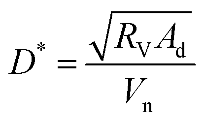 , where Ad is the effective area. The noise of PTE detectors mainly comes from the Johnson–Nyquist noise that can be expressed as,
 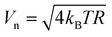 ,39 where the Boltzmann constant is 1.9 × 10⁻²³ J K−1, T is the temperature and R is the device resistance. The trends of responsivity match with the responsivity. The detector indicates a maximum detectivity of 2.2 × 10⁸ Jones. The maximum detectivity of 2.2 × 10⁸ Jones locates the blackbody peak wavelength of 3.3 μm. Generally, the thermoelectric properties of the materials do not change with the ambient radiation peak wavelength. Thus, the reason may be that both drop-cast MXene films show an internal infrared absorption at around 3.3 μm. The competitive PTE response may have several reasons. First, the reduced CNT channel may approximate the cooling length of hot carriers, which mostly maximizes the performance. Second, the top MXene electrode may absorb most of the infrared radiation, which helps achieve rapid and effective PTE conversion. Compared with our previous work, although the traditional CNTF can absorb the infrared radiation almost completely, the heating process may occur in the whole CNTF channel instead of the CNT tip region.27 Third, without the introduction of polymers, the thermal loss may be reduced and the effective thermoelectric conversion may be increased.31 Fourth, the CNTF grown by PECVD may be mainly composed of MWCNTs with a positive Seebeck coefficient of about 30 μV.40 The CNTF grown by low-pressure CVD may be mixed p-/n-type SWCNTs, which may significantly hinder the thermoelectric capacity and even reduce the PTE conversion efficiency.27 Furthermore, with a larger gap among CNTs, the PECVD-grown CNTF can be easily quantified and designed as the typical number according to specific requirements.
Top electrode influence
We also measure the influence of electrode thickness by adjusting the dropping volume of 25 mg mL−1 MXene solution. When the dropped solution volume is 10/20/30 μL, the thickness of Ti3C2 or Mo2C film is 0.9/1.8/2.7 μm or 1.2/2.4/3.6 μm, respectively (Fig. 4). Such thin MXene thicknesses indicate the dense deposition and excellent dispersion of the MXene solution. With the 873 K blackbody radiation temperature, the photovoltage of both PTE detectors shows a decreasing trend with the increase in electrode thickness. We contribute the reasons to the PTE conversion limitations, which means the MXene electrode of typical thickness can achieve a photothermal conversion. Once the top electrode thickness exceeds the typical value, the MXene of extra thickness may act as a heat sink and significantly reduce the thermal energy utilization efficiency of the CNTF. MXene films have been investigated as electromagnetic radiation shielding. For the thick films, the MXene may act as the radiation shielding material and cannot achieve effective photothermal conversion. Thus, only the MXene with typical thickness can realize effective photothermal conversion. Once the top MXene electrode thickness exceeds the typical value, the MXene of extra thickness may act as a heat sink and significantly reduce the thermal energy utilization efficiency of the CNTF. | ||
| Fig. 4 Relationship between photovoltage and (a) electrode types, (b) electrode thickness of the Ti3C2 film and (c) Mo2C film. | ||
PTE detector system and NDT imaging
Then, a NDT imaging test was performed using a measurement setup (Fig. 5(a)). The blackbody radiation passed through the MIR filter. The single-pixel packaged PTE detector was fixed in a table. The MC-200 equipment will control the aluminum arrow object to move, where the step length is 500 μm. Typically, the PTFE cavity is manufactured by fill-mode laser cutting. In an environment full of nitrogen gas, the PTE detector can be sealed in the PTFE cavity using vacuum glue. According to ref. 41 and 42, most of the MIR radiation can be transmitted through the PTFE materials, and thus, PTFE can act as an excellent packaging and MIR filter material for PTE detectors. Here, the accumulated height of the PTE detector can be calculated as 525 × (1 ± 10%) μm (Si substrate) + 100.2 nm (bottom Cr electrode) + 5 μm (CNTF) + 1 μm (top MXene electrode) ≈ 530 μm. The cut depth of the PTFE cavity by laser is 1530 μm (Fig. 5(b)). Then, we measured the PTE response of the packed detector using blackbody radiation under the same experimental conditions. The photovoltage was recorded, and finally, the photovoltage was patterned according to the relative intensity (Fig. 5(d)). This experiment demonstrates the capacity of NDT imaging. Furthermore, the resolution can be further optimized by reducing the single-pixel size of the PTE detector, and this design idea paves the way for packaging wearable sensors. | ||
| Fig. 5 (a) Illustration of the measurement setup. (b) Two-dimensional illustration of the packing detector. The red arrows are the illumination source. (c) Photograph of the real object. (d) NDT PTE imaging. The schematic figures are not illustrated to scale. | ||
Stability
Given the industrial and product application in the future, the long-term stability of the PTE detectors is also crucial. Thus, we tested the PTE detectors with Ti3C2 and Mo2C top electrodes under 873 K blackbody radiation (Fig. 6(a)). The PTE responses of both detectors show relatively high degradation. The may be because the surface terminations are oxidized and influence infrared absorption and conductivity.43 The other reason may be that the contact resistance increases between MXenes and conductive silver glue because of the degradation of silver glue. The PTE responses of both detectors show relatively high degradation. The reason may be that the surface terminations are oxidized, which influences infrared absorption. Additionally, the device resistance increases and we attribute this to the increasing contact resistance between MXenes and conductive silver glue. Another reason may be that the conductivity of MXene decreases.43 Then, we tested the PTE response of the encapsulated device with PTFE (Fig. 6(b)). In comparison, the degradation was significantly suppressed after 35 days. This result indicates that the packaging will be further beneficial for large-scale industrial applications. | ||
| Fig. 6 Relationship between the time and the photovoltage of (a) Ti3C2 and (b) Mo2C electrodes with or without PTFE packaging. | ||
To assess our detector performance, we compared our detectors with other MIR detectors. Although our detectors do not show a superior response, they have shown a competitive advantage as self-powered detectors (Table. S1†). Optimizing the CNTF channel may potentially enhance the PTE response according to the thermal decay length theory.44 Additionally, patterning the MXene top electrodes toward the metamaterials may be another optimization solution.
Conclusions
In this work, we have fabricated a self-powered vertical PTE detector working in the MIR regime. This detector adopted CNTFs as the PTE channel as well as MXenes as the top electrode. We characterized the PTE response related to the two types of MXene electrodes and their electrode thickness. The MXene electrodes showed an excellent stable ohmic contact with the CNTF. With the blackbody temperature of 873 K, the detector demonstrated a detectivity of 2.2 × 10⁸ Jones. Ultimately, we packed our PTE detector into a PTFE system and performed the NDT test, which indicated a response degradation delay and competitive imaging capacity.Overall, this PTE detector integrated with a vertical CNTF channel and MXene electrodes achieves broadband infrared detection. Unlike the laser source, the blackbody radiation source will illuminate a relatively large range, which provides a higher response challenge for the device. Our scalable detector can accept large-area radiation because the top MXene electrodes will absorb the infrared radiation and convert it into thermal energy, forming a temperature difference along the long-axis direction of the CNT and inducing thermoelectric conversion. Compared with the PTE detector using an in-plane asymmetric structure or the p–n junction, this configuration makes use of steric space and provides opportunities for device miniaturization, where we only need to consider the in-plane absorber area. Additionally, the number and height of CNT can be accurately controlled and the device performance can be quantified. The one-dimensional (1-D) CNTF also paves the path to other 1-D materials such as the nanowire array. Furthermore, the CNTF or nanowire array can be patterned into a metamaterial structure and achieve in-plane and vertical PTE optimization. The self-powered packaged PTE detectors provide new insights for the industrial long-term monitoring system and daily smart wearable sensors. Typically, the front and back sides of the smartwatch can integrate the PTE detector and achieve an energy harvester of the human body and environmental thermal radiation.
Conflicts of interest
There are no conflicts to declare.Acknowledgements
This research acknowledges the funding source of the Natural Sciences and Engineering Research Council of Canada (NSERC), CMC Microsystems, and Huawei Techniques. The authors also acknowledge Prof. Dayan Ban's blackbody radiation source use.References
- M. Dai, C. W. Wang, B. Qiang, F. K. Wang, M. Ye, S. Han, Y. Luo and Q. J. Wang, On-chip mid-infrared photothermoelectric detectors for full-Stokes detection, Nat. Commun., 2022, 13, 4560 CrossRef CAS PubMed.
- K. R. Jinkins, S. M. Foradori, V. Saraswat, R. M. Jacobberger, J. H. Dwyer, P. Gopalan, A. Berson and M. S. Arnold, Aligned 2D carbon nanotube liquid crystals for wafer-scale electronics, Sci. Adv., 2021, 7, 37 CrossRef PubMed.
- X. Du and K. Zhang, Recent progress in fibrous high-entropy energy harvesting devices for wearable applications, Nano Energy, 2022, 101, 107600 CrossRef CAS.
- D. Kireev, K. Sel, B. Ibrahim, N. Kumar, A. Akbari, R. Jafari and D. Akinwande, Continuous cuffless monitoring of arterial blood pressure via graphene bioimpedance tattoos, Nat. Nanotechnol., 2022, 17, 864–870 CrossRef CAS PubMed.
- S. Gehr and C. Russmann, Shaping the future of cardiovascular medicine in the new era of wearable devices, Nat. Rev. Cardiol., 2022, 19, 501–502 CrossRef PubMed.
- D. A. Bandurin, E. Mönch, K. Kapralov, I. Y. Phinney, K. Lindner, S. Liu, J. H. Edgar, I. A. Ditriev, P. Jarillo-Herrero, D. Svintsov and S. D. Ganichev, Cyclotron resonance overtones and near-field magnetoabsorption via terahertz Bernstein modes in graphene, Nat. Phys., 2022, 18, 462–467 Search PubMed.
- X. Cai, A. B. Sushkov, R. J. Suess, M. M. Jadidi, G. S. Jenkins, L. O. Nyakiti, R. L. Myers-Ward, S. Li, J. Yan, D. K. Gaskill, T. E. Murphy, H. D. Drew and M. S. Fuhrer, Sensitive room-temperature terahertz detection via the photothermoelectric effect in graphene, Nat. Nanotechnol., 2014, 9, 814–819 CrossRef CAS PubMed.
- W. Guo, Z. Dong, Y. Xu, C. Liu, D. Wei, L. Zhang, X. Shi, C. Guo, H. Xu, G. Chen, L. Wang, K. Zhang, X. Chen and W. Lu, Sensitive Terahertz Detection and Imaging Driven by the Photothermoelectric Effect in Ultrashort-Channel Black Phosphorus Devices, Adv. Sci., 2020, 7, 5 Search PubMed.
- W. Lu, Z. Fan, Y. Yang, J. Ma, J. Lai, X. Song, X. Zhuo, Z. Xu, J. Liu, X. Hu, S. Zhou, F. Xu, J. Cheng and D. Sun, Ultrafast photothermoelectric effect in Dirac semimetallic Cd3As2 revealed by terahertz emission, Nat. Commun., 2022, 13, 1623 CrossRef CAS PubMed.
- Y. Cao, J. Zhu, J. Xu, J. He, J. Sun, Y. Wang and Z. Zhao, Ultra-Broadband Photodetector for the Visible to Terahertz Range by Self-Assembling Reduced Graphene Oxide-Silicon Nanowire Array Heterojunctions, Small, 2014, 10, 2345–2351 CrossRef CAS PubMed.
- K. Zhang, B. Ouyang, Y. Wang, Y. Xia and Y. Yang, Coupling Enhancement of Photo-Thermoelectric Conversion in a Lateral ZnO Nanowire Array, ACS Appl. Energy Mater., 2019, 2, 7647–7654 CrossRef CAS.
- Z. Xie, J. Wang and J. T. W. Yeow, Doped Polyaniline/Graphene Composites for Photothermoelectric Detectors, ACS Appl. Nano Mater., 2022, 5(6), 7967–7973 CrossRef CAS.
- J. Li, Y. Zou, D. Hu, Y. Gu, Z. Han, J. Liu and X. Xu, et al., Enhanced room-temperature terahertz detection and imaging derived from anti-reflection 2D perovskite layer on MAPbI3 single crystals, Nanoscale, 2022, 14, 6109–6117 RSC.
- M. Zhang and J. T. W. Yeow, Flexible Polymer-Carbon Nanotube Composite with High-Response Stability for Wearable Thermal Imaging, ACS Appl. Mater. Interfaces, 2018, 10, 26604–26609 CrossRef CAS PubMed.
- M. Naguib, M. Kurtoglu, V. Presser, J. Lu, J. Niu, M. Heon, L. Hultman, Y. Gogotsi and M. W. Barsoum, Two-Dimensional Nanocrystals Produced by Exfoliation of Ti3AlC2, Adv. Mater., 2011, 23(37), 4248–4253 CrossRef CAS PubMed.
- M. Ghidiu, M. R. Lukatskaya, M.-Q. Zhao, Y. Gogotsi and M. W. Barsoum, Conductive two-dimensional titanium carbide ‘clay’ with high volumetric capacitance, Nature, 2015, 516, 78–81 CrossRef PubMed.
- T. Tan, X. Jiang, C. Wang, B. Yao and H. Zhang, 2D Material Optoelectronics for Information Functional Device Applications: Status and Challenges, Adv. Sci., 2020, 7, 11 Search PubMed.
- A. Sarycheva, A. Polemi, Y. Liu, K. Dandekar, B. Anasori and Y. Gogotsi, 2D titanium carbide (MXene) for wireless communication, Sci. Adv., 2018, 4(9), 1–9 Search PubMed.
- W. Tian, A. VahidMohammadi, Z. Wang, L. Ouyang, M. Beidaghi and M. M. Hamedi, Layer-by-layer self-assembly of pillared two-dimensional multilayers, Nat. Commun., 2019, 10(2558), 1–10 Search PubMed.
- J. Jeon, Y. Yang, H. Choi, J. H. Park, B. H. Lee and S. Lee, MXenes for future nanophotonic device applications, Nanophotonics, 2020, 9(7), 1831–1853 CrossRef CAS.
- L. Li, N. Zhang, M. Zhang, X. Zhang and Z. Zhang, Flexible Ti3C2Tx/PEDOT:PSS films with outstanding volumetric capacitance for asymmetric supercapacitors, Dalton Trans., 2019, 48, 1747–1756 RSC.
- H. Kim, B. Anasori, Y. Gogotsi and H. N. Alshareef, Thermoelectric Properties of Two-Dimensional Molybdenum-Based MXenes, Chem. Mater., 2017, 29, 6472–6479 CrossRef CAS.
- X. Jin, H. Li, Y. Wang, Z. Yang, X. Qi, J. Yang and Y. Wang, Ultra flexible PEDOT : PSS/Helical Carbon Nanotubes Film for All-in-One Photothermoelectric Conversion, ACS Appl. Mater. Interfaces, 2022, 14(23), 27083–27095 CrossRef CAS PubMed.
- D. Suzuki, Y. Takida, Y. Kawano and H. Minamide, Carbon nanotube-based, serially connected terahertz sensor with enhanced thermal and optical efficiencies, Sci. Technol. Adv. Mater., 2022, 23, 424–433 CrossRef CAS PubMed.
- K. Li, R. Yuasa, R. Utaki, M. Sun, Y. Tokumoto, D. Suzuki and Y. Kawano, Robot-assisted, source-camera-coupled multi-view broadband imagers for ubiquitous sensing platform, Nat. Commun., 2021, 12, 3009 CrossRef PubMed.
- D. Suzuki, Y. Ochiai and Y. Kawano, Thermal Device Design for a Carbon Nanotube Terahertz Camera, ACS Omega, 2018, 3, 3540–3547 CrossRef CAS PubMed.
- M. Zhang, D. Ban, C. Xu and J. T. W. Yeow, Large-Area and Broadband Thermoelectric Infrared Detection in a Carbon Nanotube Black-Body Absorber, ACS Nano, 2019, 13, 13285–13292 CrossRef CAS PubMed.
- Y. Wang, Y. Niu, M. Chen, J. Wen, W. Wu, Y. Jin, D. Wu and Z. Zhao, Ultrabroadband, Sensitive, and Fast Photodetection with Needle-Like EuBiSe3 Single Crystal, ACS Photonics, 2019, 6(4), 895–903 CrossRef CAS.
- T. J. Echtermeyer, P. S. Nene, M. Trushin, R. V. Gorbachev, A. L. Eiden, S. Milana, Z. Sun, J. Schliemann, E. Lidorikis, K. S. Novoselov and A. C. Ferrari, Photothermoelectric and photoelectric contributions to light detection in metal-graphene-metal photodetectors, Nano Lett., 2014, 14(7), 3733–3742 CrossRef CAS PubMed.
- X. He, N. Fujimura, J. M. Lloyd, J. Erickson, A. A. Talin, Q. Zhang, W. Gao, Q. Jiang, Y. Kawano, R. H. Hauge, F. Léonard and J. Kono, Carbon nanotube terahertz detector, Nano Lett., 2014, 14(7), 3953–3958 CrossRef CAS PubMed.
- J. Wang, Z. Xie, J. A. Liu and J. T. W. Yeow, Design of room-temperature infrared photothermoelectric detectors based on CNT/PEDOT:PSS composites, J. Mater. Chem. C, 2022, 10, 15105–15113 RSC.
- A. Szabó, A. Pavao, P. Zsuzsanna, G. Tamás, N. Krisztián, H. Endre, F. László and H. Klara, Growth of CNT Forests on Titanium Based Layers, Detailed Study of Catalysts, Front. Chem., 2018, 6, 2296–2646 Search PubMed.
- S.-J. Choi, P. Bennett, K. Takei, C. Wang, C. C. Lo, A. Javey and J. Bokor, Short-Channel Transistors Constructed with Solution-Processed Carbon Nanotubes, ACS Nano, 2013, 7(1), 798–803 CrossRef CAS PubMed.
- X. He, F. Léonard and J. Kono, Uncooled Carbon Nanotube Photodetectors, Adv. Opt. Mater., 2015, 3, 989–1011 CrossRef CAS.
- S. Seyedin, J. Zhang, K. A. S. Usman, S. Qin, A. M. Glushenkov, E. R. S. Yanza, R. T. Jones and J. M. Razal, Facile Solution Processing of Stable MXene Dispersions towards Conductive Composite Fibers, Global Challenges, 2019, 3(10), 1900037 CrossRef PubMed.
- V. Jourdain and C. Bichara, Current understanding of the growth of carbon nanotubes in catalytic chemical vapour deposition, Carbon, 2013, 58, 2–39 CrossRef CAS.
- J. Liu, D. Jiang, Y. Fu and T. Wang, Carbon nanotubes for electronics manufacturing and packaging: From growth to integration, Adv. Manuf., 2013, 1, 13–27 CrossRef.
- X. Guan, W. Feng, X. Wang, R. Venkatesh and J. Ouyang, Significant Enhancement in the Seebeck Coefficient and Power Factor of p-Type Poly(3,4-ethylenedioxythiophene):Poly(styrenesulfonate) through the Incorporation of n-Type MXene, ACS Appl. Mater. Interfaces, 2020, 12, 13013–13020 CrossRef CAS PubMed.
- W. Wu, Y. Wang, Y. Niu, P. Wang, M. Chen, J. Sun, N. Wang, D. Wu and Z. Zhao, Thermal Localization Enhanced Fast Photothermoelectric Response in a Quasi-One-Dimensional Flexible NbS3 Photodetector, ACS Appl. Mater. Interfaces, 2020, 12(12), 14165–14173 CrossRef CAS PubMed.
- D. Suzuki, Y. Ochiai, Y. Nakagawa, Y. Kuwahara, T. Saito and Y. Kawano, Fermi-level-controlled semiconducting-separated carbon nanotube films for flexible terahertz imagers, ACS Appl. Nano Mater., 2018, 1(6), 2469–2475 CrossRef CAS.
- A. M. S. Galante, O. L. Galante and L. L. Campos, Study on application of PTFE, FEP and PFA fluoropolymers on radiation dosimetry, Nucl. Instrum. Methods Phys. Res., Sect. A, 2010, 619, 177–180 CrossRef CAS.
- J.-Y. Park, J.-H. Lee, C.-H. Kim and Y.-J. Kim, Fabrication of polytetrafluoroethylene nanofibrous membranes for guided bone regeneration, RSC Adv., 2018, 8, 34359–34369 RSC.
- A. Iqbal, J. Hong, T. Y. Ko and C. M. Koo, Improving oxidation stability of 2D MXenes: synthesis, storage media, and conditions, Nano Convergence, 2021, 8, 9 CrossRef CAS PubMed.
- S. Nanot, A. W. Cummings, C. L. Pint, A. Ikeuchi, T. Akiho, K. Sueoka, R. H. Hauge, F. Léonard and J. Kono, Broadband, Polarization-Sensitive Photodetector Based on Optically-Thick Films of Macroscopically Long, Dense and Aligned Carbon Nanotubes, Sci. Rep., 2013, 3, 1335 CrossRef PubMed.
Footnote |
| † Electronic supplementary information (ESI) available. See DOI: https://doi.org/10.1039/d2na00895e |
| This journal is © The Royal Society of Chemistry 2023 |