 Open Access Article
Electrical transport properties of TiO2/MAPbI3 and SnO2/MAPbI3 heterojunction interfaces under high pressure†
Yuqiang Li *ad,
Yuhong Liad,
Qiang Zhangb,
Xiaofeng Liuc,
Yuanjing Liad,
Ningru Xiaoe,
Pingfan Ningd,
Jingjing Wangad,
Jianxin Zhangad and
Hongwei Liuad
aTianjin Key Laboratory of Optoelectronic Detection Technology and Systems, School of Electronic and Information Engineering, Tiangong University, Tianjin 300387, China. E-mail: liyuqiang@tiangong.edu.cn
bKey Laboratory of Smart Grid of Ministry of Education, School of Electrical and Information Engineering, Tianjin University, Tianjin 300072, China
cTianjin San'an Optoelectronics Co., LTD, Tianjin 300384, China
dEngineering Research Center of High Power Solid State Lighting Application System of Ministry of Education, Tiangong University, Tianjin 300387, China
eSchool of Physical Science and Technology, Tiangong University, Tianjin 300387, China
First published on 23rd January 2023
Abstract
The electrical transport properties of SnO2(TiO2)/MAPbI3 (MA = CH3NH3+) heterojunction interfaces are investigated from ambient pressure to 20 GPa, and the transport properties are calculated by physical parameters such as trap energy density, binding energy, and charge transfer driving force and defect. Based on the partial density of states (PDOS) of the SnO2/MAPbI3 heterojunction interface MAI-termination and PbI2-termination, greater charge transfer driving force and higher binding energy are observed, obviously showing the SnO2-based heterojunction is more stable. The SnO2/MAPbI3 heterojunction interface possesses stronger electrical transport ability and is less prone to capture electrons compared with the TiO2/MAPbI3 heterojunction interface. The differential charge density spectrum shows that the density is lower in the trap energy level of SnO2/MAPbI3, whilst the effect of the charge transfer defect is weaker owing to the trap energy level only existing in SnO2. The SnO2/MAPbI3 heterostructure interface is less prone to capture electrons. The greater electron concentration difference is attributed to oxygen vacancy (Vo0) in the SnO-like environment, resulting in superior electron transport ability compared with the TiO-like environment.
1. Introduction
In the field of PSCs (perovskite solar cells), the interface problem is one of the key factors to determine efficiency and stability.1–3 MAPbI3 thin films can form heterojunction interfaces with TiO2 or SnO2, which will cause lattice distortion in the interface, affect electrical transport properties, and accelerate ion migration.4–6 TiO2 and SnO2 respectively form electrical transport complexes O2–Ti4+ and O2–Sn4+.7,8 SnO2 is considered a substitute for TiO2 due to its high electron mobility,9 transmittance, and stability,10–12 and less IV hysteresis. However, the band matching of SnO2/MAPbI3 is worse than that of TiO2/MAPbI3.13,14 Generally, the comparative analysis of PSC efficiency for the SnO2/MAPbI3 and TiO2/MAPbI3 electron transport layers is complex.Leijtens et al.15 reported that oxygen adsorption instability acted on the electrical transport characteristics of the TiO2/MAPbI3 heterojunction surface under the excitation of ultraviolet light, because the holes on the valence band of TiO2 recombine with the electrons at the oxygen adsorption point, resulting in the release of adsorbed oxygen molecules, forming a free electron and a positively charged oxygen vacancy on the conduction band. Yang et al.16 reported a method of drastically improving solar cell efficiency by surface optimization of the TiO2 electron transport layer (ETL) using a special ionic-liquid (IL), which shows high optical transparency and superior electron mobility. Shin et al.17 found a low-temperature colloidal method for depositing La-doped BaSnO3 films as a replacement for TiO2 to reduce ultraviolet-induced damage, and the solar cells retained over 90% of their initial performance after 1000 hours of full sun illumination. Giordano et al.18 demonstrated that Li-doped TiO2 electrodes exhibit superior electronic properties, by reducing electronic trap states enabling faster electron transport. Guo et al.19 proposed that a SnO2:InCl3 ETL was used in planar PSCs to simultaneously dope the ETL and passivate the defects at the ETL/perovskite interface, which expands the ETL/perovskite interface optimization work by using anions and cations for passivation and doping, respectively. Park20 demonstrated that trap density in the MAPbI3 close to TiO2 was far lower than that without TiO2, evidenced by the gate voltage-dependent threshold voltage difference based on the field effect transistor (FET) structure. Kim et al.21 elucidated the atomistic origin of efficient electron extraction and long stability of SnO2 based PSCs through the analysis of band alignment, carrier injection, and interfacial defects in the SnO2/MAPbI3 interface using first-principles calculations at the Perdew–Burke–Ernzerhof (PBE0) + spin–orbit-coupling (SOC) + Tkatchenko–Scheffler (TS) dispersion-correction (PBE0-SOC-TS) level for all possible terminations and MA directions.
So far, most of the studies have focused on the enhancement of the electron mobility of SnO2(TiO2)/MAPbI3 heterojunction interfaces by passivation and doping under ambient conditions and the interface oxygen vacancy induced by temperature and light. The electrical transport characteristics of SnO2(TiO2)/MAPbI3 heterojunction interfaces under high pressure are rarely studied. High pressure has been proven to be a clean and powerful tool to analyze the physical properties of various heterojunction interfaces.22,23 In this article, the electrical transport properties of SnO2(TiO2)/MAPbI3 heterojunction interfaces are investigated from ambient to 20 GPa pressure by theoretical calculations, and the transport properties are investigated using physical parameters such as trap energy density, binding energy, charge transfer driving force and defects, and charge-capture rate. The electron transport abilities of SnO2(TiO2)/MAPbI3 heterojunction interfaces are compared through the driving force of charge transfer, trap level density, and charge transfer defects calculations, using PDOS and differential charge density spectra under different pressures up to 20 GPa.
2. Theoretical basis and methods
We perform the noncollinear density functional theory (DFT) calculations with the hybrid PBE0 functional24 including TS dispersion correction25 using the Vienna Ab initio Simulation Package (VASP)26 with dipole corrections. This is because the PBE0 functional can describe the band alignment of our system very well. In order to choose suitable exchange–correlations, we complete band gap calculation for SnO2, TiO2, and MAPbI3 with different exchange–correlations using the PBE0-SOC-TS. We note that regardless of the exchange–correlation, the theoretical band gap is larger in TiO2, whereas the experimental band gap is larger in SnO2.21 Therefore, instead of choosing different exchange–correlations for the SnO2/MAPbI3 and TiO2/MAPbI3 interfaces, we select only one potential for the whole interface calculations which can minimize the average band gap error. Since the PBE0-SOC-TS gives the minimum band gap error compared with the experimental band gap, we choose the PBE0-SOC-TS exchange–correlation. We uncover the mechanism behind the superior SnO2- (TiO2-)based PSCs by employing first-principles calculations using the PBE0-SOC-TS level for the SnO2(TiO2)/MAPbI3 interface system owing to the lowest average band gap error. The projection augmented wave (PAW) method is used to carry out relevant calculations, using the Kohn–Sham (KS) equation based on density functional theory DFT,27,28 a comparative study is performed on the ETL of SnO2/MAPbI3 and TiO2/MAPbI3 heterojunction interfaces. Using the optimized SnO2(TiO2)/MAPbI3 heterojunction interface modules, energy band, PDOS, and differential charge density spectrum are calculated from ambient pressure to 20 GPa.Corresponding to the homologous electron-capture mechanism, the optimized models of the TiO2/MAPbI3 and SnO2/MAPbI3 heterojunction interfaces are shown in Fig. 1(a) and (b), respectively. The parameters of SnO2(TiO2)/MAPbI3 heterojunction interface models are set (Table S3 in ESI†). The crystal cells on the surfaces of the [001], [011] and [111] plane SnO2 and TiO2, and [001] plane cubic MAPbI3 are studied at 0 GPa, 5 GPa, 10 GPa, and 15 GPa. The slab consists of symmetric SnO2 or TiO2 (5 layers, 22 Sn/Ti atoms, and 44 O atoms) and MAPbI3 [001], [011] and [111] (3 layers; MAI-termination: 4 MA molecules, 3 Pb atoms, and 10 I atoms; PbI2-termination: 3 MA molecules, 4 Pb atoms, and 11 I atoms), where the lattice mismatches of SnO2(TiO2)/MAPbI3 heterojunction interface models are as small as ∼2.75% with a vacuum size of ∼40 Å. Atomic coordinates of √2 × √2 supercells of SnO2(TiO2)/MAPbI3 heterojunction interface models are shown in Tables S1 and S2 in the ESI.† Considering the lattice parameters of pristine SnO2 (√2 × √2 supercell) and MAPbI3 (√2 × √2 supercell) are about 6.55 and 6.25 Å, respectively, the average lattice parameter of 6.4 Å is selected which makes the lattice mismatch of both sides 2.75%. With combinations of MAI- and PbI2-terminations with [001], [011], and [111] directions of MA in MAPbI3, six types of SnO2/MAPbI3 (Fig. S2(a)–(c) in the ESI†) and TiO2/MAPbI3 (Fig. S2(d)–(f) in the ESI†) heterojunction interfaces are investigated under high pressure up to 20 GPa. Using the GCA-PBE functional, the truncation energy is set to 500 eV and the sampling density at point K is set to 3 × 3 × 5. The convergence standard of structural optimization is that the difference in energy iteration is less than 1 × 10⁻⁶ eV per atom, the maximum force of atom is less than 0.02 eV A−1, and DFT+U is set. To reduce the lattice mismatch between MAPbI3 and TiO2 or SnO2 in the DFT calculations, the initial distance between the four layers of atoms in the outermost layer of MAPbI3 and TiO2 or SnO2 is set to 3.05 Å, and the vacuum layer at the heterojunction interface is set to 10.05 Å. Using the optimized TiO2/MAPbI3 and SnO2/MAPbI3 heterojunction interface models, the optimized Pb–I bond is relaxed from the original 3.15 Å to 3.45 Å, the length of the Ti–I bond and Sn–I bond is 3.38 Å, and the Pb–O bond is 2.35 Å. The area of the SnO2(TiO2)/MAPbI3 heterojunction interface is selected to be about 1.68 nm2. The optimized SnO2/MAPbI3 heterojunction interface shows stronger interface bonding and interface atom interaction.
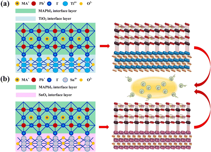 | ||
| Fig. 1 Optimized models and structures of (a) TiO2/MAPbI3 heterojunction interface, (b) SnO2/MAPbI3 heterojunction interface, showing electron-capture mechanism similarly. | ||
3. Results and discussion
For the optimized SnO2(TiO2)/MAPbI3 heterojunction interface modules, the interface binding energy of the two heterojunction interface models is:| ΔE(SnO2(TiO2)/MAPbI3) = E(TiO2)/E(SnO2) + E(MAPbI3) − E(SnO2(TiO2)/MAPbI3) | (1) |
 | (2) |
The MAPbI3 model and SnO2(TiO2) models of SnO2(TiO2)/MAPbI3 heterojunction interfaces are optimized and calculated by static-self consistent calculations, and van der Waals force is introduced to correct them. The binding energy of SnO2/MAPbI3 [ΔEunit(SnO2/MAPbI3) = −1.02 eV nm−2] is significantly higher than the binding energy of TiO2/MAPbI3 [ΔEunit(TiO2/MAPbI3) = −6.75 eV nm−2] under ambient conditions (Table S4 in ESI†), which shows that the structure of the SnO2/MAPbI3 heterojunction interface is more stable. The SnO2/MAPbI3 heterojunction interface has higher interface binding energy, showing stronger interface atom interactions and more stable heterojunction interface structure The difference in binding energy is smaller with applied pressure up to 20 GPa since the binding energy of the SnO2/MAPbI3 heterojunction interface increases less (Table S5 in ESI†). Compared with the TiO2/MAPbI3 heterojunction interface, the larger interfacial binding energy of the SnO2/MAPbI3 heterojunction interface roughly keeps the stable Pb–I bond leading to improvement in electrical transport properties.29–31
The PDOS of MA, Pb, I, Ti, Sn, and O in the TiO2/MAPbI3 and SnO2/MAPbI3 heterojunction interfaces are shown in Fig. 2(a)–(f) under different pressures, respectively. For the TiO2/MAPbI3 heterojunction interface, the Fermi level is at the top of the valence band and the width of the band gap is about 0.75 eV. The bottom CBM (Conduction Band Minimum) of the conduction band of TiO2 is basically composed of the valence electrons of Ti atoms, and the bottom CBM of MAPbI3 is mainly composed of the valence electrons of Pb atoms. Similarly, the VBM (Valance Band Maximum) at the left side of the Fermi level, that is, the valence band top of TiO2, is mainly composed of the valence electrons of O atoms, and the VBM at the valence band top of MAPbI3 is mainly composed of the valence electrons of I. The electronic DOS of MA atomic groups is far away from the Fermi level, and there are no peaks near the VBM and the CBM.32,33 Most of the electron transport exists between the Pb–I framework and TiO2, and MA atomic groups basically do not participate in the electron transport between the interfaces.34–36 Ti forms a chemical bond with I in MAPbI3, and electrons are transported from the surface of MAPbI3 to TiO2.37–40 The Fermi energy level is at the top of the valence band, and the right side of the Fermi energy level, which is the bottom CBM of SnO2, is basically composed of the valence electrons of Sn atoms, while the bottom CBM of MAPbI3 is mainly the valence electrons of Pb atoms, as shown in Fig. 2(a)–(c). Similarly, the VBM of SnO2 on the left side of the Fermi energy level is mainly composed of the valence electrons of O atoms, and the VBM of MAPbI3 is mainly composed of the valence electrons of I. It is also analyzed that the electronic density of states of the MA atomic group is far away from the Fermi level, and there is no wave peak near the top of the VBM and the bottom of the CBM. Therefore, most of the electron transfer exists between the Pb–I skeleton and SnO2, and the MA atomic group does not participate in the charge transfer between interfaces. Through the formation of a chemical bond between Sn and I in MAPbI3, electrons are transferred from the MAPbI3 surface to the SnO2 surface. On the surface of Pb–I, the force of interface atoms is Pb–O atomic force. On the right side of the Fermi energy level is the bottom CBM of TiO2 which is basically composed of valence electrons of Ti atoms, and the bottom CBM of MAPbI3 is mainly composed of valence electrons of Pb atoms, as shown in Fig. 2(d)–(f). Similarly, the top VBM of TiO2 on the left side of the Fermi energy level is mainly composed of the valence electrons of O atoms, and the top VBM of MAPbI3 is mainly composed of the valence electrons of I. The electronic state density of the MA atomic group is far away from the Fermi energy level, and there is no wave peak near the top VBM and the bottom CBM. Therefore, most of the electron transfer exists between the Pb–I skeleton and TiO2. The MA atomic group does not participate in the charge transfer between interfaces. The electron transfers from the MAPbI3 surface to the TiO2 surface through the chemical bond formed between O and Pb in MAPbI3. The charge transport driving force of TiO2/MAPbI3 heterostructure interfaces Ed(TiO2/MAPbI3) is:
| ΔEd(TiO2/MAPbI3) = CBM(MAPbI3) − CBM(TiO2) | (3) |
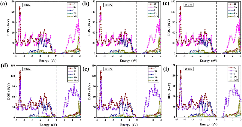 | ||
| Fig. 2 PDOS of MA, Pb, I, Sn, O at (a) 0 GPa, (b) 10 GPa, (c) 20 GPa, and MA, Pb, I, Ti, O at (d) 0 GPa, (e) 10 GPa, (f) 20 GPa. Set Fermi energy level at 0 eV. | ||
For the SnO2/MAPbI3 heterojunction interface, the bottom CBM of the conduction band of SnO2 is basically composed of the valence electrons of Sn atoms, and the bottom CBM of MAPbI3 is mainly the valence electrons of Pb atoms.41,42 The electronic DOS of the MA atomic group is also far away from the Fermi level, and no peak is observed near the VBM and CBM. Most of the electron transport exists between the Pb–I skeleton and SnO2, and the MA atomic group basically does not participate in the electron transport between heterostructure interfaces. Electrons are transported from the surface of MAPbI3 to the surface of SnO2 through the formation of a chemical bond between O and Pb in MAPbI3.43 The charge transport driving force of SnO2/MAPbI3 heterojunction interfaces Ed(SnO2/MAPbI3) is:
| ΔEd(SnO2/MAPbI3) = CBM(MAPbI3) − CBM(SnO2) | (4) |
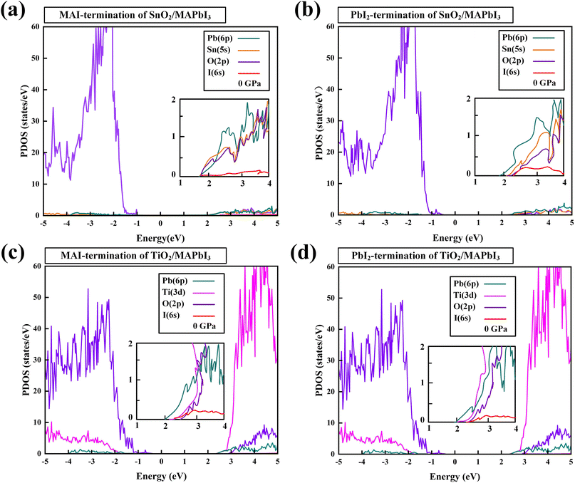
The PDOS of SnO2/MAPbI3 and TiO2/MAPbI3 heterojunction interfaces in MAI-termination and PbI2-termination are shown in Fig. 3(a)–(d). The CBMs of SnO2, TiO2, and MAPbI3 are mostly composed of Sn-5s, Ti-3d, and Pb-6p, respectively. The CBM orbital hybridizations occur between Sn-5s and Pb-6p orbitals at the SnO2/MAPbI3 interface and between Ti-3d and Pb-6p at the TiO2/MAPbI3 interface. The binding energies on the MA orientations of [001], [011] and [111] of MAI-termination and PbI2-termination SnO2/MAPbI3 and TiO2/MAPbI3 are obtained (Tables S7–S10 in ESI†).
The binding energy of the PbI2-termination of the SnO2/MAPbI3 heterojunction interface is greater than that of MAI-termination under different pressures, showing in the orbital hybridization of Pb (MAPbI3) and Sn (SnO2) interface atoms at the PbI2-termination, which is conducive to efficient electron extraction. The orbital hybridization in the SnO2/MAPbI3 heterojunction interface is greater than that in TiO2/MAPbI3 owing to that the d orbital does not strongly hybridize with the s orbital or p orbital generally.44,45 We note that the orbital hybridization difference is closely related to the carrier injection performance of the SnO2(TiO2)/MAPbI3 heterostructure interfaces, showing that the SnO2/MAPbI3 heterojunction interface has better carrier injection due to the greater orbital hybridization compared with that at the TiO2/MAPbI3 heterojunction interface.21
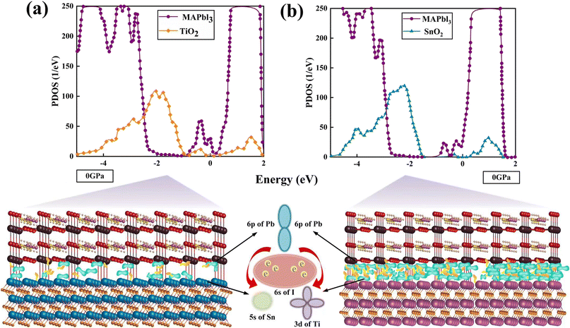
The DOS of the SnO2(TiO2)/MAPbI3 heterojunction interfaces are calculated to verify the SnO2/MAPbI3 heterojunction interface effectively reduces the trap energy level compared with the TiO2/MAPbI3 heterojunction interface under ambient conditions, as shown in Fig. 4(a) and (b). The trap energy levels in the interface band gaps of SnO2/MAPbI3 and TiO2/MAPbI3 heterojunction interfaces are used as the carrier binding center in the process of interface charge transfer.46 The trap density is approximately 23.4% lower than that of the TiO2/MAPbI3 heterojunction interface, attributed to the trap energy level only existing in SnO2 for the SnO2/MAPbI3 heterojunction interface. The SnO2/MAPbI3 heterojunction interface effectively reduces the defects affecting interface charge transfer and the trap energy level to reduce carrier recombination, which almost eliminates the interface defects caused by interface action in perovskites. The electron-capture rate of the TiO2/MAPbI3 heterojunction interface is approximately 27.5% more than that of SnO2/MAPbI3. Compared with the TiO2/MAPbI3 heterojunction interface, the SnO2/MAPbI3 heterostructure interface is less prone to capture electrons.
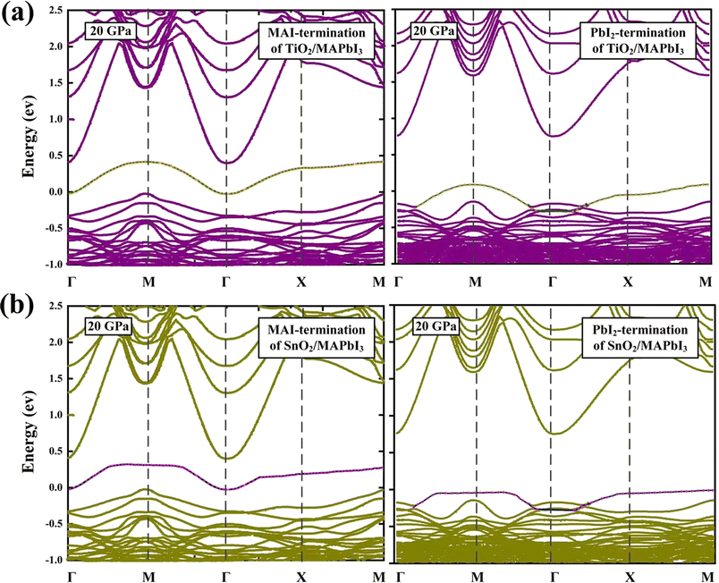
The band structures of the TiO2/MAPbI3 and SnO2/MAPbI3 heterojunction interfaces with Vo0 are shown in Fig. 5(a) and (b) at 20 GPa. Corresponding to the PDOS of Fig. 4(a) and (b), the zero of energy represents the top of the valence band for the MAI-termination and PbI2-termination of the TiO2/MAPbI3 and SnO2/MAPbI3 heterojunction interfaces. The green and orange alternative circles indicate the contribution of the surface Ti-5s states. The surface becomes a TiO-like environment attributed to the Vo0 which makes the Ti-5s state almost filled with electrons.47 For the MAI-termination and PbI2-termination of SnO2/MAPbI3, the contribution of the surface Sn-5s states is shown by the pink and blue alternative circles. The surface becomes a SnO-like environment due to the Vo0 filling the Sn-5s state with electrons. The SnO-like environment has better electron filling density, showing a superior electron transport environment compared with the TiO-like environment. The electron concentration difference in the SnO-like environment will be greater, which will result in greater electron transport ability compared with the TiO-like environment.
4. Conclusions
The SnO2/MAPbI3 heterojunction interface shows superior electrical transport properties compared with the TiO2/MAPbI3 heterostructure interface up to 20 GPa, manifested in the density of trap energy levels, binding energy, charge transfer driving force and defects, and charge-capture rate. The trap energy level of SnO2/MAPbI3 only exists in SnO2, and the density of the trap energy level (23.4%) is much lower. The charge transfer driving force of the SnO2/MAPbI3 heterojunction interface (1.45 eV) is greater than that of TiO2/MAPbI3 (0.75 eV). The binding energy (−1.02 eV nm−2) of the SnO2/MAPbI3 heterojunction interface is significantly higher than that of TiO2/MAPbI3 (−6.75 eV nm−2), showing the obviously more stable SnO2-based heterojunction structure. The electron-capture rate of the TiO2/MAPbI3 heterojunction interface is approximately 27.5% more than that of SnO2/MAPbI3. Compared with the TiO2/MAPbI3 heterojunction interface, the SnO2/MAPbI3 heterostructure interface is less prone to capture electrons, which is shown by the greater electron concentration difference in the SnO-like environment attributed to Vo0 compared with the TiO-like environment.Conflicts of interest
There are no conflicts to declare.Acknowledgements
This work was supported by the National Natural Science Foundation of China (Grant Nos. 11804249, 61804107), and the Natural Science Foundation of Tianjin City (Grant Nos. 18JCQNJC03700, 18JCYBJC85400, 20JCQNJC00180).References
- B. O'Regan and M. Grätzel, Nature, 1991, 353, 737–740 CrossRef.
- A. L. Linsebigler, G. Lu and J. T. Yates, Chem. Rev., 1995, 95, 735–758 CrossRef CAS.
- U. Bach, D. Lupo, P. Comte, J. E. Moser, F. Weissörtel, J. Salbeck, H. Spreitzer and M. Grätzel, Nature, 1998, 395, 583–585 CrossRef CAS.
- E. Mosconi, E. Ronca and F. D. Angelis, J. Phys. Chem. Lett., 2014, 5, 2619–2625 CrossRef CAS PubMed.
- J. Jeng, Y. Chiang, M. Lee, S. Peng, T. Guo, P. Chen and T. Wen, Adv. Mater., 2013, 25, 3727–3732 CrossRef CAS PubMed.
- J. H. Heo, S. H. Im, J. H. Noh, T. N. Mandal, C. S. Lim, J. A. Chang, Y. H. Lee, H. J. Kim, A. Sarkar, M. K. Nazeeruddin, M. Gratzel and S. I. Seok, Nat. Photonics, 2013, 7, 486–491 CrossRef CAS.
- J. Haruyama, K. Sodeyama, I. Hamada, L. Han and Y. Tateyama, J. Phys. Chem. Lett., 2017, 8, 5840–5847 CrossRef CAS PubMed.
- K. C. Ko, S. T. Bromley, J. Y. Lee and F. Illas, J. Phys. Chem. Lett., 2017, 8, 5593–5598 CrossRef CAS PubMed.
- J. Jeon, T. Eom, E. Lee, S. Kim, S. Kim, K.-H. Hong and H. Kim, J. Phys. Chem. C, 2017, 121, 9508–9515 CrossRef CAS.
- C. Motta, F. E. Mellouhi, S. Kais, N. Tabet, F. Alharbi and S. Sanvito, Nat. Commun., 2015, 6, 7026 CrossRef CAS PubMed.
- F. Zheng, L. Z. Tan, S. Liu and A. M. Rappe, Nano Lett., 2015, 15, 7794–7800 CrossRef CAS PubMed.
- C. W. Myung, S. Javaid, K. S. Kim and G. Lee, ACS Energy Lett., 2018, 3, 1294–1300 CrossRef CAS.
- F. D. Angelis, D. Meggiolaro, E. Mosconi, A. Petrozza, M. K. Nazeeruddin and H. J. Snaith, ACS Energy Lett., 2017, 2, 857–861 CrossRef.
- K. Oh, K. Jung, J. Shin, S. Ko and M.-J. Lee, J. Mater. Sci. Technol., 2021, 92, 171–177 CrossRef CAS.
- T. Leijtens, G. E. Eperon, S. Pathak, A. Abate, M. M. Lee and H. J. Snaith, Nat. Commun., 2013, 4, 2885 CrossRef PubMed.
- D. Yang, X. Zhou, R. Yang, Z. Yang, W. Yu, X. Wang, C. Li, S. F. Liu and R. Chang, Energy Environ. Sci., 2016, 9, 3071–3078 RSC.
- S. S. Shin, E. J. Yeom, W. S. Yang, S. Hur, M. G. Kim, J. Im, J. Seo, J. H. Noh and S. I. Seok, Science, 2017, 356, 167–171 CrossRef CAS PubMed.
- F. Giordano, A. Abate, J. P. C. Baena, M. Saliba, T. Matsui, S. H. Im, S. M. Zakeeruddin, M. K. Nazeeruddin, A. Hagfeldt and M. Graetzel, Nat. Commun., 2016, 7, 10379 CrossRef CAS PubMed.
- X. Guo, J. Du, Z. Lin, J. Su, L. Feng, J. Zhang, Y. Hao and J. Chang, Chem. Eng. J., 2021, 407, 127997 CrossRef CAS.
- B. Park, Results Phys., 2021, 23, 104025 CrossRef.
- J. Kim, K. S. Kim and C. W. Myung, npj Comput. Mater., 2020, 6, 100 CrossRef CAS.
- Y. Chen, Y. He, J. Wang, M. Li, M. Yu, R. Ye, B. Geng, Z. Yang, X. Zeng and J. Hu, J. Phys. Chem. Lett., 2021, 12, 989–996 CrossRef CAS PubMed.
- Y. Li, J. K. Cooper, R. Buonsanti, C. Giannini, Y. Liu, F. M. Toma and I. D. Sharp, J. Phys. Chem. Lett., 2015, 6, 493–499 CrossRef CAS PubMed.
- J. P. Perdew, K. Burke and M. Ernzerhof, Phys. Rev. Lett., 1996, 77, 3865 CrossRef CAS PubMed.
- A. Tkatchenko and M. Scheffler, Phys. Rev. Lett., 2009, 102, 073005 CrossRef PubMed.
- G. Kresse and J. Furthmuller, Comput. Mater. Sci., 1996, 6, 15 CrossRef CAS.
- Y. Guo, Y. Xue and L. Xu, Comput. Mater. Sci., 2021, 187, 110081 CrossRef CAS.
- L. Wang, F. Si, F. Tang and H. Xue, Mater. Res. Express, 2019, 6, 026312 CrossRef.
- R. A. Kerner and B. P. Rand, J. Phys. Chem. Lett., 2017, 8, 2298–2303 CrossRef CAS PubMed.
- S. Ito, S. Tanaka and H. Nishino, J. Phys. Chem. Lett., 2015, 6, 881–886 CrossRef CAS PubMed.
- F. Zheng, L. Z. Tan, S. Liu and A. M. Rappe, Nano Lett., 2015, 15, 7794–7800 CrossRef CAS PubMed.
- F. Zhang, S. Y. Park, C. Yao, H. Lu, S. P. Dunfield, C. Xiao, S. Uličná, X. Zhao, L. D. Hill, X. Chen, X. Wang, L. E. Mundt, K. H. Stone, L. T. Schelhas, G. Teeter, S. Parkin, E. L. Ratcliff, Y.-L. Loo, J. J. Berry, M. C. Beard, Y. Yan, B. W. Larson and K. Zhu, Science, 2022, 375, 71–76 CrossRef CAS PubMed.
- D. Liu and T. L. Kelly, Nat. Photonics, 2014, 8, 133–138 CrossRef CAS.
- S. Zhang, J. Su, J. Zhang, Z. Lin, H. Yuan, J. Chang and Y. Hao, J. Phys. Chem. Lett., 2021, 12, 11834–11842 CrossRef CAS PubMed.
- E. P. Mukhokosi and M. Maaza, J. Mater. Sci., 2022, 57, 1555–1580 CrossRef CAS.
- J. M. Azpiroz, E. Mosconi, J. Bisquert and F. D. Angelis, Energy Environ. Sci., 2015, 8, 2118 RSC.
- W. Shi and H. Ye, J. Phys. Chem. Lett., 2021, 12, 4052–4058 CrossRef CAS PubMed.
- K. Yan, Z. Wei, T. Zhang, X. Zheng, M. Long, Z. Chen, W. Xie, T. Zhang, Y. Zhao and J. Xu, Adv. Funct. Mater., 2016, 26, 8545–8554 CrossRef CAS.
- J. Zhang, K. Wang, Q. Yao, Y. Yuan, J. Ding, W. Zhang, H. Sun, C. Shang, C. Li, T. Zhou and S. Pang, ACS Appl. Mater. Interfaces, 2021, 13, 29827–29834 CrossRef CAS PubMed.
- C. Yang, P. Du, Z. Dai, H. Li, X. Yang and Q. Chen, ACS Appl. Mater. Interfaces, 2019, 11, 14044–14050 CrossRef CAS PubMed.
- T. Liu, L. Liu, M. Hu, Y. Yang, L. Zhang, A. Mei and H. Han, J. Power Sources, 2015, 293, 533–538 CrossRef CAS.
- J. Yan, Z. Lin, Q. Cai, X. Wen and C. Mu, Choline chloride-modified SnO2 achieving high output voltage in MAPbI3 perovskite solar cells, ACS Appl. Energy Mater., 2020, 3, 3504–3511 CrossRef CAS.
- J. H. Heo and S. H. Im, Nanoscale, 2016, 8, 2554–2560 RSC.
- C. Li, J. Hu, S. Wang, J. Ren, B. Chen, T. Pan, X. Niu and F. Hao, J. Phys. Chem. Lett., 2021, 12, 4569–4575 CrossRef CAS PubMed.
- Y. Ai, Y. Zhang, J. Song, T. Kong, Y. Li, H. Xie and D. Bi, J. Phys. Chem. Lett., 2021, 12, 10567–10573 CrossRef CAS PubMed.
- G. S. H. Thien, N. A. Talika, B. K. Yap, H. Nakajima, S. Tunmee, N. Chanlek and B. T. Goh, Ceram. Int., 2020, 46, 29041–29051 CrossRef CAS.
- T. Bu, J. Li, F. Zheng, W. Chen, X. Wen, Z. Ku, Y. Peng, J. Zhong, Y. Cheng and F. Huang, Nat. Commun., 2018, 9, 4609 CrossRef PubMed.
Footnote |
| † Electronic supplementary information (ESI) available. See DOI: https://doi.org/10.1039/d2ra08143a |
| This journal is © The Royal Society of Chemistry 2023 |

