
 Open Access Article
 This Open Access Article is licensed under a Creative Commons Attribution-Non Commercial 3.0 Unported Licence
Electronic and valleytronic properties of crystalline boron-arsenide tuned by strain and disorder
L. Cracoa,
S. S. Cararaa,
E. da Silva Barbozaa,
M. V. Milošević ab and
T. A. S. Pereira*a
ab and
T. A. S. Pereira*a
aInstitute of Physics, Federal University of Mato Grosso, 78060-900, Cuiabá, MT, Brazil. E-mail: teldo@fisica.ufmt.br
bDepartment of Physics, University of Antwerp, Groenenborgerlaan 171, 2020 Antwerp, Belgium
First published on 13th June 2023
Abstract
Ab initio density functional theory (DFT) and DFT plus coherent potential approximation (DFT + CPA) are employed to reveal, respectively, the effect of in-plane strain and site-diagonal disorder on the electronic structure of cubic boron arsenide (BAs). It is demonstrated that tensile strain and static diagonal disorder both reduce the semiconducting one-particle band gap of BAs, and a V-shaped p-band electronic state emerges – enabling advanced valleytronics based on strained and disordered semiconducting bulk crystals. At biaxial tensile strains close to 15% the valence band lineshape relevant for optoelectronics is shown to coincide with one reported for GaAs at low energies. The role played by static disorder on the As sites is to promote p-type conductivity in the unstrained BAs bulk crystal, consistent with experimental observations. These findings illuminate the intricate and interdependent changes in crystal structure and lattice disorder on the electronic degrees of freedom of semiconductors and semimetals.
I. Introduction
Boron arsenide (BAs) crystallizes in the zinc-blende phase (depicted in Fig. 1), which is isostructural with other III–V semiconductors such as GaAs, and is a p-type semiconductor as-grown.1 Compared to other III–V zinc-blende-type compounds, BAs had until recently not been considered suitable for applications due to difficulties with synthesizing high-quality single crystals. However, recent fabrication of highly pure samples of cubic BAs, and subsequent measurement of high room temperature thermal conductivity (in the range from 900 to 1300 W mK−1 (ref. 2)), have placed BAs at the forefront of materials research for future optoelectronic3–5 as well as photo-electrochemical6 applications. More precisely, within the context of electronic and optoelectronic materials, cubic BAs is expected to be useful for ultrahigh thermal management,7 one of the prime challenges when operating electronic devices. Additionally, its low density, large resistivity, its isoelectronic configuration to that of Si, and feasible alloying with GaAs,8 all open doors to versatile microelectronic applications of BAs.9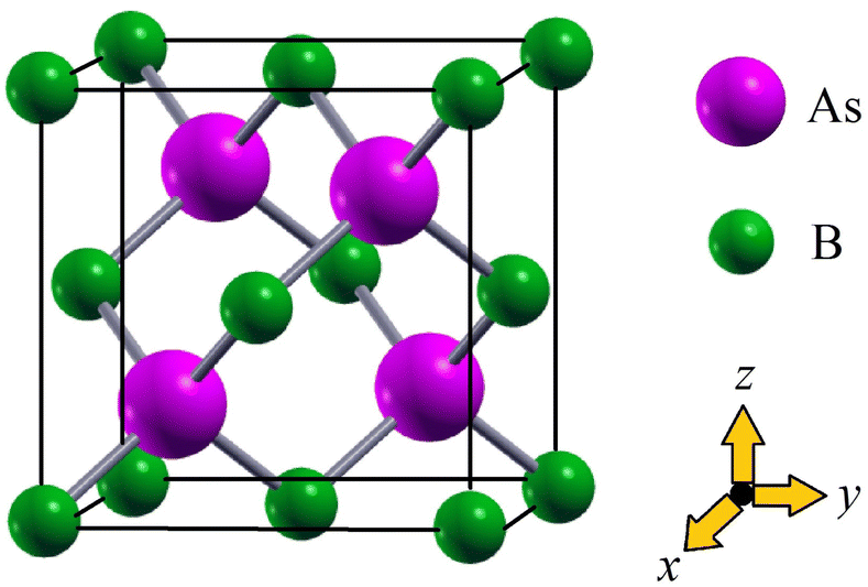 | ||
| Fig. 1 Schematic unit cell of the zinc-blende-type crystal structure of cubic BAs bulk crystal. B and As are represented as small and large spheres, respectively. | ||
Experimental studies to date have indicated an inherent band gap between 1.46 and 2.1 eV in cubic BAs bulk crystal.6,10–12 Computational studies using density functional theory (DFT) revealed that the band structure of BAs is similar to other boron pnictides13 as well as to GaAs.14 Moreover, a previous theoretical work has shown the absence of negative frequencies in the phonon dispersion, providing support to the stability of BAs crystal.15 In BAs the conduction band minimum occurs along the Γ-to-X direction and has p-band character, in contrast to AlAs, GaAs, or InAs, where the s-like conduction band minimum is found at the Γ-point. The difference may be attributed to the low energy position of the p orbitals of boron ions,8 as a result of strong covalence between B and As. Moreover, according to earlier DFT studies, the indirect band gap, as well as the lowest direct band gap (at Γ), could be substantially different depending on the theory and approximations applied, with estimated values being between 0.7 and 2.07 eV.12,16 For the sake of clarity, we shall mention here ref. 17 which explore the role played by different exchange-correlation functionals and spin–orbit coupling, showing that the band gap of BAs crystal can vary from 1.197 to 1.717 eV. Here, based on generalized gradient approximation (GGA) we estimate an indirect gap of 1.22 eV. This result agrees well with the values computed in earlier GGA calculations,18,19 which also slightly underestimates the band gap of the BAs bulk crystal.
For both fundamental and applied purposes it is worth noting here that the relationship between the energy of an electron and its momentum is determined by the band structure of the system, with the local minimum in the conduction band and local maximum in the valence band being referred to as valley,20 whose topology is governed by the crystal structure and chemical composition of the material. Thus, in addition to orbital, charge and spin, electrons in semiconductors and semimetals may also host valley degrees of freedom.21 Similar to spin in spintronics,22 the valley degree of freedom opens the possibility to store and carry information, leading to an emerging device concept for electronic applications now known as valleytronics.23,24 In valleytronic materials24 electrons can populate low-energy valley states (or inequivalent local energy extrema),20 providing an additional quantum index which introduces forefront paradigms to quantum information processing.25 In addition to traditional semiconductors, such as AlAs,26 which have multiple valleys in the conduction bands located near the high symmetry points in the Brillouin zone, earlier works have reported tunable electronic structure and valley polarization of Dirac fermion sytems,21 such as graphene,27 bismuth,28 and Cd3As2.29 One of the most documented tuning knobs is the lattice strain, widely used in the semiconductor electronics industry to increase carrier mobilities.30,31 In valleytronics, strain directly affects the valley-dependent energy dispersion,20 including manipulating the band gap size of conventional semiconductors3,4,32,33 as well as of the spin-valley-coupled Dirac semimetals21 with V-shaped band dispersion near the Fermi energy, EF.
Here, based on first principles band structure calculations we report the electronic structure reconstruction of an in-plane strained cubic BAs bulk crystal, exhibiting strain-tunable band gap narrowing, and emergence of a V-shaped p-band electronic dispersion suitable for advanced valleytronics. This study is timely, as straining BAs has become a viable technological approach. Namely, in their seminal work,34 Cui et al. recently demonstrated that self-assembled cubic BAs (also referred to as s-BAs) can be highly deformable, to support uniaxial strains above 500% of its original size, similarly to homogeneous elastomers. In addition, the s-BAs can be compressed or strained to random geometries without leading to a mechanical breakdown, which recommends it for application as a thermal interface material. Thus, a thermal interface based on s-BAs with both high thermal conductivity and high flexibility is expected to find applications in flexible thermal cooling, soft robotics, among other emerging areas of flexible electronics.35
Last but not least, it is of high relevance to above mentioned applications to understand the effect of the ever-present disorder in the experimentally synthesized BAs bulk crystals on the resulting electronic properties. For that purpose, we extend our first principles calculations to include the coherent potential approximation and examine the role of point defects on As sites in the electronic properties, with special attention paid to vacancies and antisites36 – being main actors as intrinsic lattice disorder in the BAs system.37 Coupled to the observed tunability with strain, these results recommend BAs for further exploration towards advanced p-band electronics and valleytronics.
II. Results and discussion
A. Ab initio methodology and electronic structure of pristine cubic BAs
Herein, we carried out ab initio DFT calculations as implemented in the SIESTA simulation package38 to compute the electronic band structure and spectral functions of normal and strained BAs bulk crystal. The exchange and correlation part of the total energy was computed using GGA within the Perdew–Burke–Ernzerhof (PBE) functional39 along with the DZP40 basis set. Non-relativistic pseudopotentials parameterized within the Troullier–Martins formalism were also used.41 As shown in our earlier studies, these combined approximations can accurately describe the electronic properties of pristine and strained graphene42 as well as pressure-induced electronic structure reconstruction phosphorus allotropes.43 The unit cell of the cubic BAs consists of 8 atoms. For integrations over the Brillouin zone, a well-converged Monkhorst–Pack (MP) k-point mesh44 of 10 × 10 × 10 (commensurating with the lattice vectors) was used. We consider the cubic F![[4 with combining macron]](https://www.rsc.org/images/entities/char_0034_0304.gif) 3m structure of BAs with two atoms in the primitive cell and with an experimentally reported lattice parameter of a = 4.777 Å.45 In order to find the equilibrium geometry of strained BAs, we minimize the energy with respect to the cubic lattice parameter a. Moreover, for strained BAs structural relaxation was performed using the conjugate-gradient method until the absolute value of the components of the Hellman–Feynman forces were converged to within 0.03 eV Å−1. The convergence with respect to the energy cut-offs was performed and the default energy cut-off value of 200 Ry was found to be sufficient. To establish a good accuracy between our results and computational costs, the tolerance in the matrix density was set to 10−4 eV.46
3m structure of BAs with two atoms in the primitive cell and with an experimentally reported lattice parameter of a = 4.777 Å.45 In order to find the equilibrium geometry of strained BAs, we minimize the energy with respect to the cubic lattice parameter a. Moreover, for strained BAs structural relaxation was performed using the conjugate-gradient method until the absolute value of the components of the Hellman–Feynman forces were converged to within 0.03 eV Å−1. The convergence with respect to the energy cut-offs was performed and the default energy cut-off value of 200 Ry was found to be sufficient. To establish a good accuracy between our results and computational costs, the tolerance in the matrix density was set to 10−4 eV.46
In Fig. 3 we show the atom- and band-resolved density-of-states (DOS) of cubic BAs bulk crystal calculated using the GGA within the valence configurations 2s22p1 and 4s24p3 for B and As, respectively. As seen in the left upper panel, due to strong covalence the valence and conduction bands are nearly equally composed by both boron and arsenic p-type orbitals at low energies, with the valence band maximum almost reaching EF. The conduction band is also mostly governed by threefold degenerate p-band electronic states, with the conduction band minimum being located at energies close to 1.2 eV above EF. As visible in the lower left panel, valence band of cubic BAs has significant additional s-type contributions from both B and As at high binding energies. As mentioned above and consistent with earlier studies,16,18,47 the size of the indirect band gap determined from our electronic band structure calculation for unstrained BAs crystal is 1.22 eV, as shown in Fig. 2. Finally, the p-type semiconducting nature intrinsic to cubic BAs bulk crystal is also manifested in total DOS (Fig. 3, right panel), where a small amount of hole doping would naturally introduce dominant p-band carriers in the electrical conductivity.47
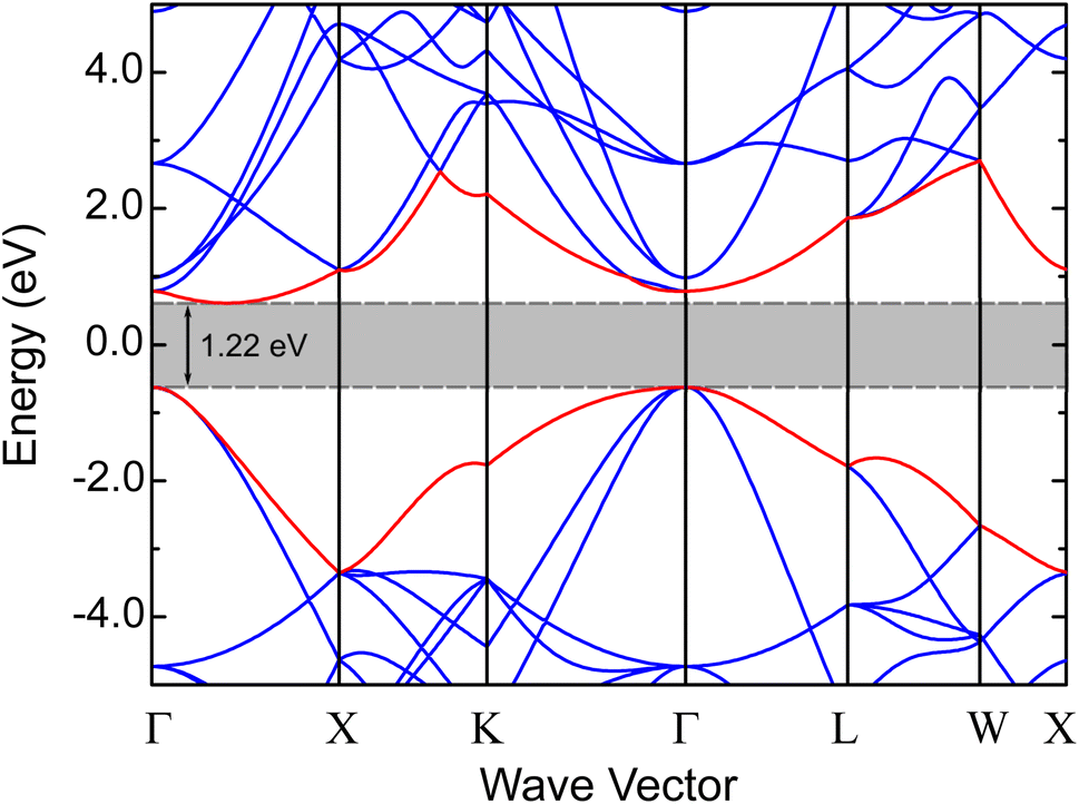 | ||
| Fig. 2 Electronic band structure of unstrained BAs bulk crystal. Notice the 1.22 eV indirect gap between the Γ and X directions of the first Brillouin zone. | ||
 | ||
| Fig. 3 Partial (left) and total (right) density of states (DOS) of the cubic BAs bulk crystal. Notice the nearly similar p-band DOS near the Fermi energy EF = ω = 0 due to large p-band hybridization. [In the right panel a vertical dashed line at ω = 0 marks the position of the Fermi energy.] | ||
B. Tunability by strain
It is now recognized that under external perturbations such as pressure or lattice strain the hopping elements of pnictides semiconductors and semimetals, including the one-particle band gap, can be renormalized in diverse and rather non-trivial ways.3,13,21,48 We recall here, for example, the work by Liu et al.,21 showing that the one-particle band gap of functionalized SbAs monolayers has a non-intuitive dependence on strain, where the band gap decreases gradually to zero and then increases with increasing elastic strain. Also interesting in this context is the study of the BAs heterostructure by Bushick et al.,3 showing that isotropic biaxial in-plane strain and pressure decrease the band gap size. Moreover, based on atomistic calculations it has been predicted in ref. 3 that 1% biaxial tensile strain increases the in-plane electron and hole mobilities at 300 K by more than 60% as compared to the unstrained BAs, due to reduced electron effective masses and hole interband scattering processes. Finally, the effect of biaxial strain on the electronic properties of hexagonal BAs single-layer (h-BAs) has been studied theoretically in ref. 49, by applying strains from 2 to 14%, to reveal that this mono-layer material behaves as a direct band gap semiconductor for strains up to 8%; the band gap of h-BAs changes from direct to indirect, and its size decreases with further increasing strain. Interestingly, this 2D-like system becomes metallic under biaxial strain of 14%. Latter semiconductor–metal transition is caused by the lowering of the conduction band, reaching EF at the threshold strain of ∼12%. Below, we show that similar electronic structure evolution is characteristic also of strained BAs bulk crystals.Fig. 4 shows the atom- and orbital-resolved p-band DOS of BAs as a function of the in-plane biaxial lattice strain. Several interesting and distinguishing features are seen in this figure, when compared to the unstrained spectral function. First, there is an overall downshift of the conduction band states toward lower energy values, while the valence band maximum is stabilized and almost pinned at energies very close to EF. Second, the intensity of the lowest-energy van Hove-like peak in the pz DOS of B and As progressively grows with increasing strain. Third, and more surprisingly, a V-shaped like DOS characteristic of Dirac semimetals emerges near the semiconducting–semimetallic electronic transition, as seen in our results for the atom-resolved pz DOS at 10% strain in Fig. 4. Also remarkable is the lifting of the orbital degeneracy characteristic of cubic BAs bulk crystal, with the pz orbital showing distinct spectral features as compared to the twofold degenerate px,y orbitals. As visible in Fig. 4, the valence and conduction band spectra show appreciable one-particle band narrowing with increasing strain. Interesting as well, and consistent with earlier calculations for single-layer boron pnictides,13 are our results for the total DOS in the main panel of Fig. 5, showing how the occupied and unoccupied Dirac-like V-band lineshape progressively emerges in BAs with increasing in-plane biaxial strain.
 | ||
| Fig. 4 Effect of strain on the atom- (left panel B, right As) and orbital-resolved p-band DOS of the BAs bulk crystal. Notice the lowering of the conduction band states and the systematic reduction of the band gap with increasing strain. | ||
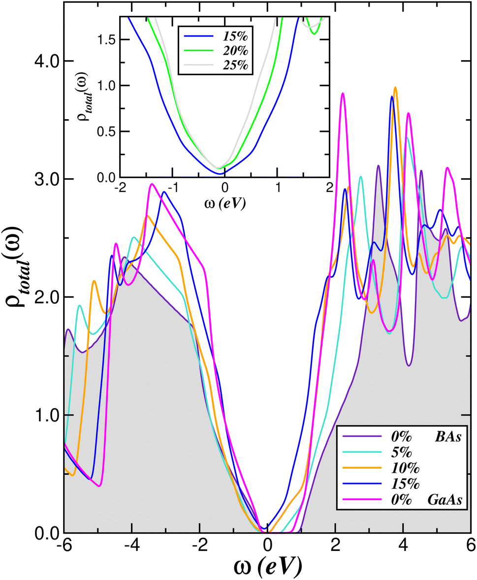 | ||
| Fig. 5 Effect of biaxial lattice strain on the total DOS of a BAs bulk crystal. Notice the slightly larger band gap of BAs as compared to GaAs51 and the nearly similar valence (conduction) band low-in-energy lineshape between 15% (10%) strained BAs and the unstrained GaAs semiconductor.51 Also noteworthy is the resulting nearly linear V-shaped spectra at large strains, shown in the inset. | ||
To better visualize the systematic evolution of the nearly V-shaped one-particle spectral function of strained BAs, in the inset of Fig. 5 we display the total spectra for the in-plane biaxial strain between 15 and 25%. As seen, upon increasing strain a consistent trend is observed in our reconstructed spectral functions, with the V-like total DOS being less particle–hole asymmetric and closely following a linear behavior in the energy range of ±2.0 eV. According to this result, an all-electron semimetallic electronic state with characteristic akin to Dirac fermion systems13 is predicted to emerge in highly strained BAs bulk crystals.
C. Assisted effect of disorder
Owing to the importance of BAs bulk crystal for technological applications, we recall here that cubic BAs is known to incorporate high concentrations of crystal imperfections that can act as sources of p-type conductivity.47 The latter has been attributed to the formation of native defects due to experimental grown conditions50 as well as to unintentional acceptor impurities such as silicon and carbon, all potent to induce p-band conductivity. Interestingly, low temperature photoluminescence measurements of BAs bulk crystals revealed impurity-related recombination processes (including donor–acceptor pair recombination).47 It has also been found in ref. 47 that B impurities can be incorporated on the As sites, forming electrical antisite complexes. Finally, it has been reported theoretically that vacancies and antisites are rather typical point defects in BAs bulk crystals,36 both acting as intrinsic lattice disorder in the system.37In what follows, we, therefore, focus on the effects of site-diagonal disorder in the As electronic states of a BAs bulk crystal. Here, we treat the disordered BAs within the DFT plus coherent potential approximation (DFT + CPA), which allows for an exact treatment of binary disorder in the limit of high lattice dimensions.52,53 Generally speaking, our scheme is the uncorrelated limit of that applied to the disordered Hubbard model,52 where the effect of site-diagonal disorder is modeled by incorporating an Anderson-like disorder term  (ref. 54) in the bare one-electron Hamiltonian of BAs bulk crystal, which reads
  . Here, a = x, y, z labels the diagonalized p-bands, εa(k) is the one-electron band dispersion, which encodes details of the one-electron (GGA) band structure, μ is the chemical potential, and ε(0)a are on-site orbital energies of pristine and strained BAs, whose bare values are read off from the GGA spectral functions. In the spirit of ref. 52 and 55 we restrict ourselves to a binary-alloy distribution for disorder, therefore the disorder potentials vi at the As sites are specified by the probability distribution P(vi) = (1 − x)δ(vi) + xδ(vi − δ), meaning that upon incorporation of chemical disorder a fraction x of As sites will have an additional local potential δ for an electron hopping onto that site. In other words, the As-4p carriers of BAs bulk crystal experience different local environments in the course of their hopping, and the physical object which accounts for this effect is the CPA.52,56 The detailed formulation of the disordered problem treated within CPA52 has already been developed and used in the context of p-band semiconductors57 and semimetals,58 so we do not repeat the equations here.
Fig. 6 shows the changes in the electronic structure of an unstrained BAs bulk crystal, for different disorder parametrization. The δ values used in this work are taken from the center of gravity of the B (4.9 eV) and As (2.3 eV) total DOS, and in our CPA calculations they correspond to antisite defects (i.e., B ions on As sites) as well to As vacancies, whose deep-trap level59 is assumed to be the negative of As center of gravity. The most salient feature to be seen in the panels of Fig. 6 is that sizable electronic reconstruction is predicted to emerge in unstrained BAs due to site-diagonal disorder effects with increasing the concentration x of disordered As lattice sites. Particularly interesting is the emergence of p-type conductivity47 upon incorporation of B-antisite defects. This is characterized by the appearance of low-energy electronic states in the reconstructed DOS near EF.
 | ||
| Fig. 6 Effect of site-diagonal disorder in the As total DOS of pristine BAs bulk crystal. Notice the changes in the electronic lineshape with increasing the concentration x of local disorder. The lower and upper panels display, respectively, the effect of disorder due to B-antisites (δ = 4.9 eV) and As-vacancies (δ = −2.3 eV). | ||
Even more interesting, however, are our results in Fig. 7, showing the changes in the electronic structure of disordered BAs bulk crystals for the two values of δ mentioned above, for fixed disorder fraction x = 0.1. As seen, strong electronic reconstruction is predicted to emerge due to the combined effect of site-diagonal disorder and lattice strain, inducing p- and n-band conductivity upon incorporation of B-antisite defects (lower panel) and As-vacancies (upper panel). What lies at the origin of these low-energy features? In a disordered system, incoherent scattering between different carriers in orbital states leads to site- and orbital-dependent shifts of the p-bands relative to each other, and renormalized scattering rates60 due to sizable δ cause appreciable spectral weight transfer over large energy scales, from high to low energies. This leads to a self-consistent modification of the spectral lineshape, as shown in Fig. 6 and 7. In accordance with earlier studies,52,58,60,61 broadening-induced quantitative changes in the electronic structure reduce the band gap and modify the low-energy electronic lineshape near EF, both in normal (Fig. 6) and highly strained (Fig. 7) BAs bulk crystal. As visible in Fig. 7, the interplay between strain and incoherent scattering arising from B-antisites and As-vacancies yields the emergence of pseudogapped spectral functions in strained BAs with similarities akin to disordered Dirac liquids: the incoherent semimetal found upon application of strains above 10% is thus predicted to be the counterpart of the marginal Dirac liquid found in disordered silicene.58 More theoretical and experimental work on disordered semiconductors and semimetals62 are called for to corroborate our prediction of strain-assisted V-shaped dirty Dirac-like liquids.63
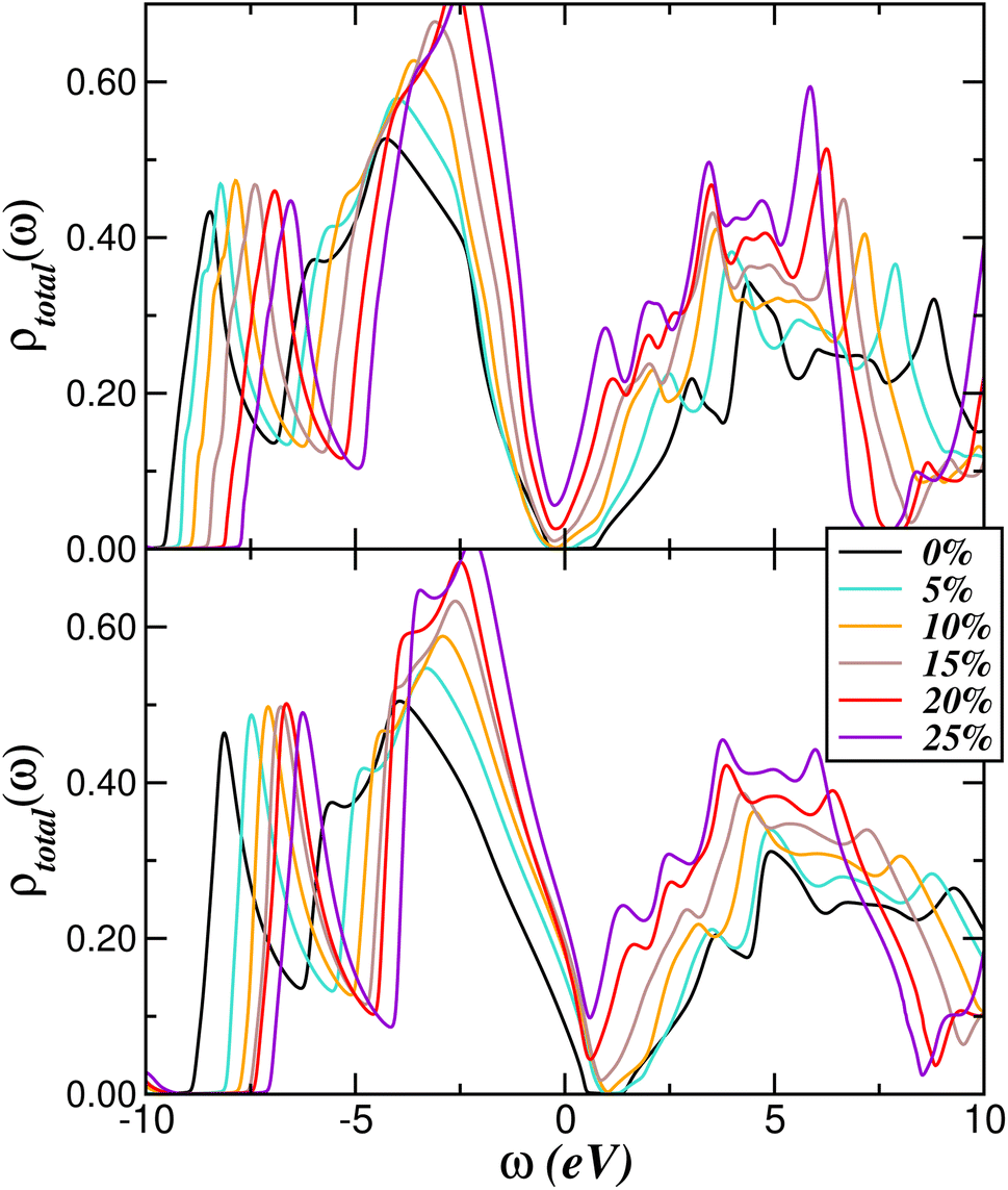 | ||
| Fig. 7 Effect of site-diagonal disorder in the As total DOS, for x = 0.1 and two different values of δ (two types of defects), for different values of biaxial strain from 5 to 25%. Notice the emergence of p- (lower panel) and n-type (upper panel) conductivity due to B-antisites (δ = 4.9 eV) and As-vacancies (δ = −2.3 eV), respectively. Noteworthy as well is the asymmetric V-shaped semimetal behavior in both panels. | ||
As a final remark, it is known that complementary electronics require both, p- and n-type semiconductors.64 Hence, according to our results in Fig. 6, disordered BAs at strains above 10% are predicted to exhibit coexisting p- and n-type semiconducting characteristics, however, of ambipolar nature since the concentrations of electron and hole carriers would not be comparable. The implications of our results in Fig. 6 are rather remarkable in our opinion, since different transport polarities are predicted to exist in one single isostructural material system. According to our results, we propose that strained BAs with chemically engineered B-antisites and As-vacancies could feature intrinsic particle-hole asymmetric differential transconductance under positive and negative gate bias. Future studies should show whether this is in fact obtained in dirty BAs (or analogues) under sizable strain conditions. Once validated, our prediction may have far-reaching implications for integrated complementary electronics and data processing capability in a single device,64 thus significantly advancing the electronic circuit design.
III. Conclusions
In summary, using first-principles calculations augmented by coherent potential approximation for disorder, we have analyzed the strain- and disorder-induced electronic reconstruction and orbital differentiation of a BAs bulk crystal. We have revealed a variety of intricate one-particle effects that arise even with moderate strain values and disorder fractions. We find that both the in-plane strain (tensile or compressive) and disorder reduce the band-gap of BAs, and both promote the electronic state containing V-shaped Dirac-like valleys at the Fermi level. In absence of strain, the kind of defects at As sites (i.e. be it arsenic vacancies or boron substitutions) determines whether the conductivity will be of p or n type.Since BAs bulk crystals are known to be stable at even extreme strains, and disorder in ever-present in grown crystals, our study provides a useful guide for future experiments. It also highlights the utility of first-principles and combined DFT + CPA calculations as fertile platforms to explore novel physical phenomena, including tuning the semiconducting band gap. This in turn opens prospects to further fundamental insights into localization–delocalization transition due to Anderson lattice disorder65 in real p-band semiconductors and semimetals.
Conflicts of interest
The authors declare that they have no conflicts of interest.Acknowledgements
This work was supported by Brazilian Agencies CNPq and CAPES, as well as by the Research Foundation-Flanders (FWO). L. C. thanks Byron Freelon and Stefano Leoni for discussion in earlier stages of this work. E. S. B. acknowledges CAPES for individual financial support.References
- T. L. Chu and A. E. Hyslop, J. Appl. Phys., 1972, 43, 276 CrossRef CAS.
- J. S. Kang, M. Li, H. Wu, H. Nguyen and Y. Hu, Science, 2018, 361, 575 CrossRef CAS PubMed; S. Li, Q. Zheng, Y. Lv, X. Liu, X. Wang, P. Y. Huang, D. G. Cahill and B. Lv, Science, 2018, 361, 579 CrossRef PubMed.
- K. Bushick, S. Chae, Z. Deng, J. T. Heron and E. Kioupakisa, npj Comput. Mater., 2020, 6, 3 CrossRef CAS.
- X. Meng, A. Singh, R. Juneja, Y. Zhang, F. Tian, Z. Ren, A. K. Singh, L. Shi, J.-F. Lin and Y. Wang, Adv. Mater., 2020, 32, 2001942 CrossRef CAS PubMed.
- R. Islam, et al., Mater. Today Commun., 2022, 33, 104227 CrossRef CAS.
- S. Wang, S. F. Swingle, H. Ye, F.-R. F. Fan, A. H. Cowley and A. J. Bard, J. Am. Chem. Soc., 2012, 134, 11056 CrossRef CAS PubMed.
- F. Pan, G. A. G. U. Gamage, H. Sun and Z. Ren, J. Appl. Phys., 2022, 131, 055102 CrossRef CAS.
- G. L. W. Hart and A. Zunger, Phys. Rev. B: Condens. Matter Mater. Phys., 2000, 62, 13522 CrossRef CAS.
- S. Chae, K. Mengle, J. T. Heron and E. Kioupakis, Appl. Phys. Lett., 2018, 113, 212101 CrossRef.
- H. Lee, G. A. Gamage, J. L. Lyons, F. Tian, B. Smith, E. R Glaser, Z. Ren and L. Shi, J. Phys. D: Appl. Phys., 2021, 54, 31LT01 CrossRef CAS.
- S. M. Ku, J. Electrochem. Soc., 1966, 113, 813 CrossRef CAS; S. Wang, S. F. Swingle, H. Ye, F.-R. F. Fan, A. H. Cowley and A. J. Bard, J. Am. Chem. Soc., 2012, 134, 11056 CrossRef PubMed.
- B. Song, K. Chen, K. Bushick, K. A. Mengle, F. Tian, G. A. G. U. Gamage, Z. Ren, E. Kioupakis and G. Chen, Appl. Phys. Lett., 2020, 116, 141903 CrossRef CAS.
- H. L. Zhuang and R. G. Hennig, Appl. Phys. Lett., 2012, 101, 153109 CrossRef CAS ; see also, R. Islam, S. lIslam, R. H. Mojumder, Z. Khan, H. Molla, A. S. M. J. Islam and J. Park, Mater. Today Commun., 2022, 33, 104227 CrossRef.
- D. N. Talwar and C. S. Ting, Phys. Rev. B: Condens. Matter Mater. Phys., 1982, 25, 2660 CrossRef CAS.
- M. Arrigoni and G. K. H. Madsen, Comput. Mater. Sci., 2019, 156, 354 CrossRef CAS.
- See, J. Buckeridge and D. O. Scanlon, Phys. Rev. Mater., 2019, 3, 051601(R) CrossRef , and references therein..
- I. Bravić and B. Monserrat, Phys. Rev. B, 2019, 3, 065402 Search PubMed.
- See, A. Rastogi, P. Rajpoot and U. P. Verma, Bull. Mater. Sci., 2019, 42, 112 CrossRef , and references therein..
- See, also, I. H. Nwigboji, Y. Malozovsky, L. Franklin and D. Bagayoko, J. Appl. Phys., 2016, 120, 145701 CrossRef , and references therein..
- J. R. Schaibley, H. Yu, G. Clark, P. Rivera, J. S. Ross, K. L. Seyler, W. Yao and X. Xu, Nat. Rev. Mater., 2016, 1, 201655 Search PubMed.
- Z. Liu, W. Feng, H. Xin, Y. Gao, P. Liu, Y. Yao, H. Weng and J. Zhao, Mater. Horiz., 2019, 6, 781 RSC.
- A. Fert, Rev. Mod. Phys., 2008, 80, 1517 CrossRef CAS.
- A. Rycerz, J. Tworzydlo and C. W. J. Beenakker, Nat. Phys., 2007, 3, 172 Search PubMed.
- See, Y. S. Ang, S. A. Yang, C. Zhang, Z. Ma and L. K. Ang, Phys. Rev. B, 2017, 96, 245410 CrossRef , and references therein..
- D. Culcer, A. L. Saraiva, B. Koiller, X. Hu and S. Das Sarma, Phys. Rev. Lett., 2012, 108, 126804 CrossRef PubMed.
- Y. P. Shkolnikov, E. P. De Poortere, E. Tutuc and M. Shayegan, Phys. Rev. Lett., 2002, 89, 226805 CrossRef CAS PubMed.
- R. V. Gorbachev, et al., Science, 2014, 346, 448 CrossRef CAS PubMed.
- B. E. Feldman, M. T. Randeria, A. Gyenis, F. Wu, H. Ji, R. J. Cava, A. H. MacDonald and A. Yazdani, Science, 2016, 354, 316 CrossRef CAS PubMed.
- C. Zhang, et al., Nat. Commun., 2017, 8, 13741 CrossRef CAS PubMed.
- S. E. Thompson, et al., IEEE Trans. Electron Devices, 2004, 51, 1790 CAS.
- K. Bushick, K. Mengle, N. Sanders and E. Kioupakisa, Appl. Phys. Lett., 2019, 114, 022101 CrossRef.
- G. Qin, Q.-B. Yan, Z. Qin, S.-Y. Yue, H.-J. Cui, Q.-R. Zheng and G. Su, Sci. Rep., 2014, 4, 6946 CrossRef CAS PubMed.
- L. Craco, S. S. Carara and S. Leoni, Phys. Rev. B, 2016, 94, 165168 CrossRef.
- Y. Cui, Z. Qin, H. Wu, M. Li and Y. Hu, Nat. Commun., 2021, 12, 1284 CrossRef CAS PubMed.
- See, D. Corzo, G. Tostado-Blázquez and D. Baran, Front. Electron., 2020, 1, 594003 CrossRef , and references therein..
- Q. Zheng, C. A. Polanco, M.-H. Du, L. R. Lindsay, M. Chi, J. Yan and B. C. Sales, Phys. Rev. Lett., 2018, 121, 105901 CrossRef CAS PubMed.
- J. Buckeridge, T. D. Veal, C. R. A. Catlow and D. O. Scanlon, Phys. Rev. B, 2019, 100, 035207 CrossRef CAS; S. Lyu, D. Skachkov, K. Kash, E. W. Blanton and W. R. L. Lambrecht, Phys. Status Solidi A, 2019, 216, 1800875 CrossRef.
- J. M. Soler, E. Artacho, J. D. Gale, A. García, J. Junquera, P. Ordejon and D. Sánchez-Portal, J. Phys.: Condens. Matter, 2002, 14, 2745 CrossRef CAS; E. Artacho, E. Anglada, O. Dieguez, J. D. Gale, A. García, J. Junquera, M. Martin, P. Ordejon, J. M. Pruneda, D. Sanchez-Portal and J. M. Soler, J. Phys.: Condens. Matter, 2008, 20, 064208 CrossRef PubMed.
- J. P. Perdew, K. Burke and M. Ernzerhof, Phys. Rev. Lett., 1996, 77, 3865 CrossRef CAS PubMed.
- P. Hohenberg and W. Kohn, Phys. Rev., 1964, 136, B864 CrossRef; W. Kohn and L. J. Sham, Phys. Rev., 1965, 140, A1133 CrossRef.
- L. Kleinman and D. M. Bylander, Phys. Rev. Lett., 1982, 48, 1425 CrossRef CAS.
- L. Craco, S. S. Carara and S. Leoni, Phys. Rev. B, 2016, 94, 165168 CrossRef.
- L. Craco, T. A. da Silva Pereira, S. R. Ferreira, S. S. Carara and S. Leoni, Phys. Rev. B, 2018, 98, 035114 CrossRef CAS.
- H. J. Monkhorst and J. D. Pack, Phys. Rev. B: Solid State, 1976, 13, 5188 CrossRef.
- R. M. Wentzcovitch and M. L. Cohen, J. Phys. C: Solid State Phys., 1986, 19, 6791 CrossRef CAS.
- The calculated lattice parameters for strained BAs are: a = b =5.0158 Å, c =4.777 Å (5% strain), a = b =5.255 Å, c =4.777 Å (10% strain) and a = b =5.494 Å, c =4.777 Å (15% strain).
- J. L. Lyons, et al., Appl. Phys. Lett., 2018, 113, 251902 CrossRef.
- F. Tian, et al., Appl. Phys. Lett., 2019, 114, 131903 CrossRef.
- K. Manoharan and V. Subramanian, ACS Omega, 2018, 3, 9533 CrossRef CAS PubMed.
- G. A. Gamage, H. Sun, H. Ziyaee, F. Tian and Z. Ren, Appl. Phys. Lett., 2019, 115, 092103 CrossRef.
- Similar result for GaAs crystal was found by S. Sanvito, P. Ordejon and N. A. Hill, Phys. Rev. B: Condens. Matter Mater. Phys., 2001, 63, 165206 CrossRef.
- M. S. Laad, L. Craco and E. Müller-Hartmann, Phys. Rev. B: Condens. Matter Mater. Phys., 2001, 64, 195114 CrossRef.
- M. S. Laad and L. Craco, J. Phys.: Condens. Matter, 2005, 17, 4765 CrossRef CAS.
- L. Craco, Solid State Commun., 2017, 253, 14 CrossRef CAS.
- K. Byczuk, M. Ulmke and D. Vollhardt, Phys. Rev. Lett., 2003, 90, 196403 CrossRef PubMed.
- See, for example, M. A. Korotin, Z. V. Pchelkina, N. A. Skorikov, E. Z. Kurmaev and V. I. Anisimov, J. Phys.: Condens. Matter, 2014, 26, 115501 CrossRef CAS PubMed.
- L. Craco, M. S. Laad and E. Müller-Hartmann, Phys. Rev. B: Condens. Matter Mater. Phys., 2003, 68, 233310 CrossRef.
- L. Craco, S. S. Carara and S. Leoni, Eur. Phys. J. B, 2021, 94, 47 CrossRef CAS.
- F. Oba and Y. Kumagai, Appl. Phys. Express, 2018, 11, 060101 CrossRef.
- M. M. Radonjić, D. Tanasković, V. Dobrosavljević and K. Haule, Phys. Rev. B: Condens. Matter Mater. Phys., 2010, 81, 075118 CrossRef.
- K. Byczuk, W. Hofstetter and D. Vollhardt, Phys. Rev. Lett., 2005, 94, 056404 CrossRef PubMed.
- S. V. Syzranov, L. Radzihovsky and V. Gurarie, Phys. Rev. Lett., 2015, 114, 166601 CrossRef CAS PubMed ; see also, A. Szabo and B. Roy, Phys. Rev. Res., 2020, 2, 043197 CrossRef.
- B. Roy and S. Das Sarma, Phys. Rev. B, 2016, 94, 115137 CrossRef.
- Y. Meng, W. Wang and J. C. Ho, ACS Nano, 2022, 16, 13314 CrossRef CAS PubMed.
- P. W. Anderson, Phys. Rev., 1958, 109, 1498 Search PubMed.
| This journal is © The Royal Society of Chemistry 2023 |