 Open Access Article
Embedding plasmonic gold nanoparticles in a ZnO layer enhanced the performance of inverted organic solar cells based on an indacenodithieno[3,2-b]thiophene-alt-5,5′-di(thiophen-2-yl)-2,2′-bithiazole-based push–pull polymer†
Alemayehu G. Waketolaa,
Cathrine Pfukwab,
Pieter Neethling b,
Gurthwin Bosmanb,
Zewdneh Genened,
Ergang Wang
 d,
Wendimagegn Mammoc,
Fekadu G. Hone
 *a and
Newayemedhin A. Tegegne
 *a
*a
aDepartment of Physics, Addis Ababa University, 1176, Addis Ababa, Ethiopia. E-mail: fekadu.gashaw@aau.edu.et; newaye.medhin@aau.edu.et
bLaser Research Institute at the Department of Physics, Stellenbosch University, 7602, Stellenbosch, South Africa
cDepartment of Chemistry, Addis Ababa University, 33658, Addis Ababa, Ethiopia
dDepartment of Chemistry and Chemical Engineering, Chalmers University of Technology, SE412 96, Goteborg, Sweden
First published on 30th May 2023
Abstract
Recently, plasmonic nanoparticles (NPs) have attracted considerable attention as good candidates for enhancing the power conversion efficiency (PCE) of organic solar cells (OSCs) owing to their localized surface plasmon resonance (LSPR). In this study, the effect of embedding colloidal gold nanoparticles (cAu NPs) in the ZnO electron transport layer (ETL) on the PCEs of wide band gap polymer-based inverted OSCs was investigated. The active layer was composed of a bulk heterojunction of conjugated polymer based on indacenodithieno[3,2-b]thiophene and 5,5′-di(thiophen-2-yl)-2,2′-bithiazole PIDTT-DTBTz as a donor and [6,6]-phenyl-C71-butyric acid methyl ester (PC71BM) as an acceptor. The PCE of the reference device was improved by 22% when 10 wt% cAu NPs were embedded in the ZnO ETL. The short circuit current density (JSC) and fill factor (FF) were the main photovoltaic parameters contributing to the PCE enhancement. An improved absorption in the active layer due to the LSPR of cAu NPs as well as efficient exciton dissociation and charge collection were found to be the reasons for the enhanced JSC while the increase in FF was mainly due to the suppressed traps and improved conductivity of the ZnO layer by the NPs.
1 Introduction
Organic solar cells (OSCs) based on bulk heterojunctions of electron-donating and accepting organic semiconductors have been at the forefront of solar cell research in the past three decades. The performances of OSCs have improved significantly and PCEs over 18% are regularly reported thanks to the intensive effort made in the synthesis of novel polymers, small molecules and device engineering.1–4 The efficiency in the absorption of light by the active layer of OSCs has been one of the focus areas in the synthesis of novel polymers and small molecules to broadly harvest a large portion of the solar spectrum. However, since organic semiconductors have low carrier mobility, the thickness of the OSC devices is usually ≈100 nm limiting the absorption of photons in the active layer. This could be improved by using metal nanoparticles (NPs) that endow a plasmonic enhancement and light trapping while keeping the device thickness in the order of free charge carriers diffusion length.5–8Nanoparticles such as Ag, Au, Cu, and Al are the commonly used plasmonic metal NPs to improve the photon harvest in OSC devices.9–13 These NPs could improve the optical absorption of OSCs in several ways that including scattering of the incident light that effectively increases its optical path length and excitation of the LSPR that increases the strength of the incident light around the materials.14–16 However, charge recombination will occur when these NPs are used in the active layer of OSC devices, which also limited their potential application in the devices.17 Plasmonic enhancement in OSCs can be achieved by embedding the NPs either in the electron transport layer (ETL), hole transport layer (HTL), the active layer, or in both in ETL and HTL.18–20 NPs embedded in the active layer can also act as recombination centers by blocking the percolation path of free charge carriers. Hence, a great deal of work has been done to improve the performance of OSCs by embedding NPs in ETLs/HTLs. Recently, we have reported a significant performance improvements in plasmonic devices by optimizing the concentration of Ag NPs in poly(3,4-ethylenedioxythiophene):poly(styrene sulfonate) (PEDOT:PSS) hole transport layer used in OSCs with normal geometry.13
Zinc oxide (ZnO) is a prominent ETL in inverted OSCs because of its simplicity in synthesis, transparency, solutions processability, compatibility with large-area fabrication techniques, good conductivity, etc.21,22 Purohit et al. and others recommended the use of ZnO buffer layer for thin film solar cell application due to its good morphological and electrical properties.21–23 Since the conduction band of ZnO (−4.4 eV) is below the lowest unoccupied molecular (LUMO) energy level of the commonly used acceptor, PC71BM (−4.0 eV), electron transfer is expected to proceed without significant energy loss. In addition, its valence band (−7.8 eV) is far below the commonly used donor polymers blocking hole transfer into ITO when used in an inverted geometry. Besides, it is more stable when exposed to the environment unlike other buffers layer such as PEDOT:PSS. However, the dangling bonds in the oxide create traps that are responsible for recombination due to the surface defects limiting its applications in optoelectronics.24,25 Doping, thermal treatment, and surface modifications using additives were some of the effective techniques used to decrease the surface defects and increase the conductivity of ZnO. Small NPs can also be embedded in the ZnO layer to improve the surface morphology while endowing the active layer with improved absorption due to their LSPR excitation.26 For example ZnO in which Ag and Au NPs are embedded has been used as ETL to improve the performance of polymer and PCBM-based OSCs.27–29 However, this kind of ETL has found limited use in OSCs based on blends of polymer and fullerene, especially under an inert atmosphere, to enhance the PCE. Thus, the effect of embedding Au in ZnO on the performance of different wide band gap polymer and fullerene blends processed in the air needs to be further explored.
Wide band gap conjugated polymers such as poly(3-hexylthiophene) (P3HT) suffer from lower absorption due to their small absorption width. Plasmonic enhancement using NPs that have resonance that matches with the absorption of these wide band gap polymers can provide a facile route for the improvement of their absorption.30,31 The bithiazole (BTz) unit has been widely used to develop push–pull type wide band gap polymers due to its weak electron-withdrawing ability, simple and planar structure, and electron-deficient nature.32,33 Our group reported the synthesis and characterization of the wide band gap push–pull polymer PIDTT-DTBTz based on the ladder-type indacenodithieno[3,2-b]thiophene (IDTT) as a donor unit and 5,5′-di(thiophen-2-yl)-2,2′-bithiazole as an acceptor unit. The polymer showed high thermal stability with a decomposition temperature of 450 °C and a PCE of 4.35% when blended with PC71BM.34 The polymer has a narrow absorption between 400 and 600 nm with an absorption maximum at 516 nm. Since the absorption maximum of PIDTT-DTBTz matches well with the resonance of small-size Au NPs (520–540 nm),35 its absorption can be improved by using such NPs which will lead to an improved charge generation in the resulting OSC devices.
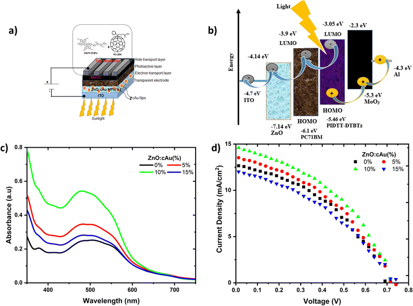
In this contribution, colloidal gold (cAu) NPs were embedded in ZnO (ZnO:cAu (%)) with weight percentages of 0, 5, 10 and 15%, to investigate the effect of the small-sized NPs both on the electrical properties of the ETL and performance of inverted OSCs. The polymer used in this study (PIDTT-DTBTz) is a wide-band gap push–pull polymer, synthesized in our group to effectively harness light absorption enhancement by the LSPR of the cAu NPs.34 Inverted OSCs with a geometry ITO/ZnO:cAu (%)/PIDTT-DTBTz:PC71BM/MoO3/Al were fabricated in ambient conditions. The PCE of the reference device (3.74%) was improved by 22%, when 10% cAu NPs were embedded in the ZnO ETLs (4.56%). This performance enhancement is mainly attributed to the increased JSC due to the improved absorption by LSPR of cAu NPs, better charge transport in the active layer, controlled surface defect and improved conductivity of ZnO layer, upon the incorporation of 10% cAu NPs. Furthermore, the PCE of the device processed in air with ZnO:cAu (10%) was slightly higher than the PCE of the device fabricated in a N2-filled glove box with a conventional device structure. Moreover, using cAu NPs embedded Zno ELT, a more stable device could be fabricated, indicating a new direction for the fabrication of air-processable OSCs with plasmonic gold nanoparticles embedded for potential commercial application.
2 Experimental section
2.1 Preparation of cAu NPs and electron transport layer
cAu NPs were synthesized by a simple solution processing method from stock solutions of gold(III) chloride trihydrate (HAuCl4·3H2O) and sodium citrate(Na3C6H5O7). Before starting the synthesis, the magnetic stirrer bar and glassware were thoroughly cleaned using aqua regia solution (HCl![[thin space (1/6-em)]](https://www.rsc.org/images/entities/char_2009.gif) :
:![[thin space (1/6-em)]](https://www.rsc.org/images/entities/char_2009.gif) HNO3 (3
HNO3 (3![[thin space (1/6-em)]](https://www.rsc.org/images/entities/char_2009.gif) :
:![[thin space (1/6-em)]](https://www.rsc.org/images/entities/char_2009.gif) 1 v/v)), and were thoroughly rinsed with distilled water and oven-dried to avoid any contamination. In a 250 mL round bottom flask attached to a condenser, a 25.4 mM solution of HAuCl4·3H2O (125 mL) was boiled under vigorous stirring at 145 °C and a 40 mM solution of sodium citrate (12.5 mL) was quickly added. The solution was further stirred for an additional 10 min, until the color of the mixture gradually changed to burgundy/maroon, which confirmed the formation of cAu. The ZnO solution was synthesized by modifying the procedure reported by Sun et al.36 Typically, a 0.52 M solution of ZnO was prepared by dissolving zinc acetate dihydrate ((CH3COO)2·2H2O) in a mixture of 2-methoxyethanol (10 mL) and ethanolamine (10 mL), which was used as a stabilizer. The solution was stirred overnight vigorously at room temperature in air. The synthesized cAu was then mixed with the dispersed ZnO solution in a weight ratio of 0, 5, 10 and 15% under stirring at room temperature for 20 min to produce ZnO electron transport layers in which cAu NPs were embedded.
1 v/v)), and were thoroughly rinsed with distilled water and oven-dried to avoid any contamination. In a 250 mL round bottom flask attached to a condenser, a 25.4 mM solution of HAuCl4·3H2O (125 mL) was boiled under vigorous stirring at 145 °C and a 40 mM solution of sodium citrate (12.5 mL) was quickly added. The solution was further stirred for an additional 10 min, until the color of the mixture gradually changed to burgundy/maroon, which confirmed the formation of cAu. The ZnO solution was synthesized by modifying the procedure reported by Sun et al.36 Typically, a 0.52 M solution of ZnO was prepared by dissolving zinc acetate dihydrate ((CH3COO)2·2H2O) in a mixture of 2-methoxyethanol (10 mL) and ethanolamine (10 mL), which was used as a stabilizer. The solution was stirred overnight vigorously at room temperature in air. The synthesized cAu was then mixed with the dispersed ZnO solution in a weight ratio of 0, 5, 10 and 15% under stirring at room temperature for 20 min to produce ZnO electron transport layers in which cAu NPs were embedded.
2.2 Device fabrication and characterization
The OSCs containing a ZnO ETL buffer layer, in which different wt% of cAu NPs were embedded, were fabricated with the structure of indium tin oxide (ITO)/ZnO:cAu (%)/PIDTT-DTBTz:PC71BM/molybdenum oxide (MoO3)/aluminum (Al). The ITO-coated glass substrates were cleaned in a boiled soap solution for 10 min, followed by rinsing and ultra-sonication in deionized water, acetone, and isopropyl alcohol (IPA) for 10 min, respectively, followed by drying in an oven. Then, the substrates were UV/ozone-treated for 30 min. The pristine and ZnO:cAu (%) ETLs were produced by spin-coating the ZnO and ZnO:cAu (%) solutions onto the pre-cleaned ITO-coated glass substrates for 60 s at 3000 rpm followed by thermal annealing at 150 °C for 60 min, and slowly cooling to room temperature. The active layer solutions were prepared by mixing PIDTT-DTBTz and PC71BM (Fig. 1) in a 1![[thin space (1/6-em)]](https://www.rsc.org/images/entities/char_2009.gif) :
:![[thin space (1/6-em)]](https://www.rsc.org/images/entities/char_2009.gif) 3 ratio in 1,2-dichlorobenzene at a concentration of 25 mg mL−1 followed by 8 h of stirring at room temperature.34 The PIDTT-DTBTz:PC71BM blend was spin coated on top of the ETLs followed by drying at 100 °C for 10 min to get a 100 nm thick active layer. Finally, a 10 nm thick MoO3 HTL followed by 100 nm thick Al, as top electrode, were deposited under high vacuum using Edward Auto 306 thermal depositor to cap the OSC devices. The area of the devices was defined by a mask to be 0.07 cm2. The current–voltage (J–V) characteristics of the OSC devices were measured using a Keithley 2400 source unit under simulated sunlight AM 1.5G spectrum (100 mW cm−2) with solar simulator system model: SS-50AA Japan, which was calibrated with a KG-5 Si diode. Electron-only devices with a structure of ITO/ZnO/PIDTT-DTBTz:PC71BM/LiF (lithium fluoride)/Al, were fabricated to investigate electron mobility in the devices.
3 ratio in 1,2-dichlorobenzene at a concentration of 25 mg mL−1 followed by 8 h of stirring at room temperature.34 The PIDTT-DTBTz:PC71BM blend was spin coated on top of the ETLs followed by drying at 100 °C for 10 min to get a 100 nm thick active layer. Finally, a 10 nm thick MoO3 HTL followed by 100 nm thick Al, as top electrode, were deposited under high vacuum using Edward Auto 306 thermal depositor to cap the OSC devices. The area of the devices was defined by a mask to be 0.07 cm2. The current–voltage (J–V) characteristics of the OSC devices were measured using a Keithley 2400 source unit under simulated sunlight AM 1.5G spectrum (100 mW cm−2) with solar simulator system model: SS-50AA Japan, which was calibrated with a KG-5 Si diode. Electron-only devices with a structure of ITO/ZnO/PIDTT-DTBTz:PC71BM/LiF (lithium fluoride)/Al, were fabricated to investigate electron mobility in the devices.
2.3 Optical, electrical and morphological characterizations
The absorbances of cAu NPs and thin films were measured using an Edinburgh instruments DS5 UV-vis/NIR spectrometer at a resolution of 2 nm. The photoluminescence (PL) spectra of thin films was carried out using a HORIBA FLUROMAX-4 spectrofluorometer. Transmission electron microscopy (TEM) measurement was carried out by using a JEOL JEM-1100 microscope equipped with a tungsten thermionic gun operating at a 100 kV accelerating voltage. Atomic force microscopy (AFM) measurement was done at room temperature in tapping mode using HA-NC A probe (12 N m−1 force and 235 kHz resonant frequency). The electrical conductivity measurements of the ZnO layer, with and without cAu NP films, prepared on ITO substrate were estimated using two probe J–V measurement systems in dark conditions.3 Result and discussion
3.1 Optical and morphological properties of cAu NPs
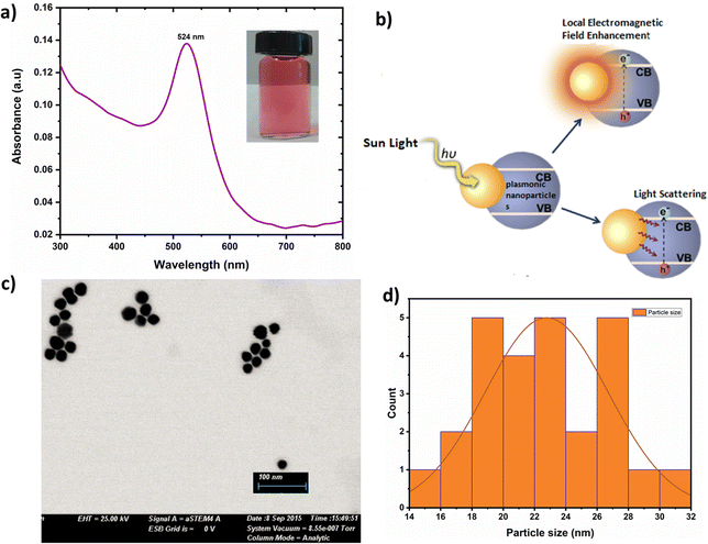
The absorption spectrum of cAu NPs depicted in Fig. 2(a) reveals an absorption maximum at 524 nm corresponding to the excitation of LSPR of the synthesized cAu NPs.37 This excitation created a standing resonance state when the wavelength of the incident light was greater than or equal to the size of the nanoparticles resulting in surface plasmon resonance as sketched in Fig. 2(b). The interaction of an electromagnetic field with the collective electrons in cAu NPs served as the basis for the formation of LSPR that can either enhance or scatter the local electromagnetic field.38 The shape of the cAu NPs was found nearly spherical with an average diameter of 22.5 nm and had relatively uniform size distribution as confirmed by their TEM images shown in Fig. 2(c) and (d).3.2 Optical and electrical properties of the ETL layer
The transmittance of an ETL plays a major role in determining the performance of inverted OSC devices. The transmittance spectra of pristine ZnO and ZnO:cAu (%), coated on glass substrates (Fig. 3(a)), confirmed that all the ETLs had good transmittance between 350 and 450 nm. Due to the absorption of cAu NPs in the visible region, the transmittance of films made by the incorporation of cAu NPs slightly decreased with increased concentration, while transmitting more than 73% of the incident light, indicating that the incorporation of cAu NPs did not significantly affect the light reaching the active layer of the OSCs.39,40 The emission of ZnO:cAu (%) was also found to increase with increasing wt% of cAu (Fig. S1†) further confirming the enhanced absorption that was responsible for the reduced transmittance of ETLs as depicted in Fig. S2.† Similar results were also reported when ZnO was doped with metals such as manganese (Mn), nickel (Ni) and silver (Ag).41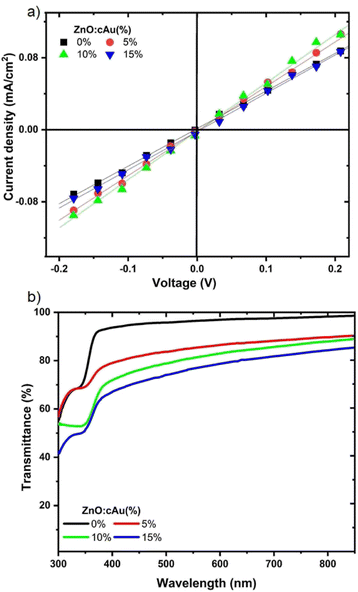 | ||
| Fig. 3 (a) Transmittance spectra and (b) electrical conductivity of ZnO ETLs with and with out cAu (%). | ||
The electrical conductivity (σ) of the ETLs were determined from the J–V measurement of ITO/ETL/Al stack using eqn (1) and the values are summarized in Table 3.
 | (1) |
3.3 Photovoltaic properties
Inverted OSCs devices were fabricated from PIDTT-DTBTz donor and PC71BM acceptor using pristine ZnO and ZnO:cAu NPs (%) as ETL with a device geometry of ITO/ZnO:cAu (%)/active layer/MoO3/Al (Fig. 4(a)). The J–V characteristics of the reference and the plasmonic devices were recorded under illumination with AM 1.5G light at 100 mW cm−2 (Fig. 4(d)). The corresponding performance parameters of the devices fabricated are summarized in Table 1. In the reference cell with pristine ZnO, an open circuit voltage (VOC) of 0.70 V, a JSC of 12.72 mA cm−2, a FF of 41.36%, and a PCE of 3.73% was obtained. A higher PCE of 4.56% was obtained when a 10% cAu NPs were embedded in the ZnO layer. The JSC of the plasmonic devices, increased when 5 and 10% cAu NPs were embedded in the ZnO ETLs. However, further increase of the cAu NP (15%) in the ZnO reduced the JSC to 12.15 mA cm−2 which was lower than the reference device. Optimized plasmonic performance was obtained when 10% cAu NPs were added in the ZnO ETL. In this device both the JSC and FF increased from 12.72 to 14.83 mA cm−2 and 41.36 to 43.02%, respectively, compared to the reference cell, while the VOC exhibited negligible change. Consequently, the PCE increased from 3.73 to 4.56% revealing a more than 22% increment. According to Usman et al., cAu Nps embedded in ZnO enhanced PCE efficiency of inverted OSCs by 24%.28 The improved performance was mainly due to higher absorbance caused by LSPR of the cAu NPs which directly affected the JSC. The devices' FF decreased as resistance increased, with the optimized device having the lowest value, indicating that the 10% cAu NPs embedded in the ZnO layer have reduced recombination losses. The increased conductivity of the ETLs was also beneficial for improved JSC, FF and PCE.The shelf-life of the reference and optimized plasmonic devices was monitored for approximately 80 h, and the evolutions of the PV parameters are shown in Fig. S5.† The device with 10% cAu NPs embedded in ZnO outperformed the reference device in terms of stability, retaining 92.6% of its initial PCE after 80 h of ageing while the reference device retained just over 82%. This demonstrates that cAu NPs can be employed as a facile route to improve the stability of OSCs.
3.4 Surface morphology of ETLs
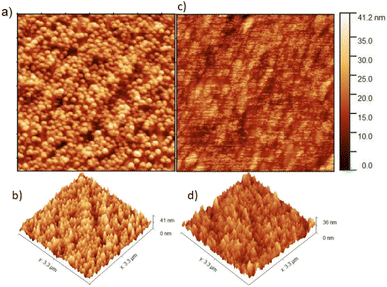
The surface morphologies of reference ZnO and ZnO:10% cAu NPs were studied using atomic force microscopy (AFM), and the obtained data were analyzed using the Gwyddion software. Fig. 7(a)–(d) shows plane and 3D views of the reference and ZnO ETL films in which 10% cAu NPs were embedded. The surface of the pristine ZnO layer revealed large grain boundaries of ZnO which were significantly reduced when the 10% cAu NPs were embedded as depicted in Fig. 7(a) and (c), respectively, reducing the surface roughness from 6.87 nm in the pristine to 5.89 nm in the optimized plasmonic device. This can be due to the disruption of the grain formation of ZnO as the cAu NPs are filling the gaps. The reduced surface defect is one of the reasons for the improved JSC in ZnO-based OSCs in which 10% cAu NPs were embedded. Similar reports also confirmed that improved surface morphology of ZnO could increase the charge collection efficiency that eventually increased the JSC.47–493.5 Charge generation and transfer kinetics
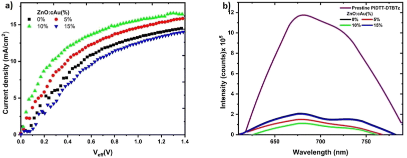
To interrogate the improvement in JSC and FF of the reference device upon incorporation of cAu NPs in the ETL, the charge generation and recombination of the reference and plasmonic devices were investigated. The photo current generated in the devices up on illumination (Jph) is dependent on the exciton generation (G), the thickness (L) and exciton dissociation probabilities P(E, T).50 Jph can be calculated from the differences of currents measured under illumination (JL) and the dark (JD) i.e., Jph = JL − JD = qGmaxLP(E, T), where q is the elementary charge and Gmax is the maximum exciton generation rate. The dark current characteristics of the devices are depicted in Fig. S3.† The plot of Jph against the effective voltage (Veff) can be used to determine the charge generation and recombination in the fabricated devices. The effective voltage is given as; Veff = Vo − V, where Vo is the voltage, where Jph is 0 and V is the applied voltage. The plot of Jph versus Veff of the devices fabricated with the reference and ZnO in which cAu NPs were embedded is given in Fig. 5(a). The Jph of the devices increased linearly in the lower Veff followed by a region where the Jph started to saturate at Jsat (saturation current).51 The saturation regions indicate that the dissociation of excitons P(E, T) has reached close to 100% and G to its maximum value, hence Jsat = qLGmax.52 The Jsat of devices were found to be 14.31, 14.8, 15.80, and 13.51 mA cm−2 for the devices fabricated using 0, 5, 10, 15% cAu NPs embedded in ZnO ETLs. The increased Jsat with 5 and 10% cAu NPs is the direct result of the increased absorption in the active layer due to the LSPR of the NPs that increased the exciton generation. Despite the higher absorption of the device in which 15% cAu NPs were embedded, the Gmax was lower than that of the reference device. This could be due to the 10% reduced transmittance by the higher concentration of the NPs in the ZnO ETL as shown in Fig. 3(a).Once the excitons are generated in the active layer, dissociation into free charges followed by percolation of free charges towards their respective electrode proceeds before charges are collected by the electrodes. The excitons that are generated in PIDTT-DTBTz polymer are quenched by PC71BM as depicted in the charge dynamics sketch in Fig. 4(b), making the charge transfer at the donor/acceptor interface a crucial parameter for efficient current generation. The exciton quenching efficiencies (QEs) of the reference and plasmonic devices were investigated using steady state PL spectroscopy (Fig. 5(b)). The QEs of the plasmonic devices were found to be higher compared to the reference cell, with the highest value found to be 90.49% for the ZnO in which 10% cAu NPs were embedded, confirming an efficient charge transfer at the donor/acceptor interface (Table 2). This efficient charge transfer can be due to an improved donor/acceptor interface and/or lowered exciton binding energy by the LSPR of the NPs. However, since the NPs were not embedded in the active layer, an improved donor/acceptor interface can be neglected. To elucidate the argument that the exciton binding might have been lowered by the LSPR of cAu NPs, we measured the electric field-dependent PL of the polymer coated on ZnO (polymer/ZnO:cAu NPs) as shown in Fig. S4.† The PL yield of the polymer coated on ZnO:cAu (10%) was reduced by more than 27% while the reference has only decreased by less than 15% at 10 V biasing voltage confirming the lowering of exciton binding energy due to the electromagnetic field around the NPs.
| ZnO:cAu (%) | QE (%) | Jph (mA cm−2) | Jsat (mA cm−2) | Gmax × 1021 (s−1 cm−3) | P(coll) (Jph/Jsat) (%) |
|---|---|---|---|---|---|
| 0 | 82.11 | 12.72 | 14.31 | 11.21 | 88.93 |
| 5 | 87.17 | 13.67 | 14.80 | 11.50 | 92.40 |
| 10 | 90.49 | 14.83 | 15.80 | 12.32 | 93.90 |
| 15 | 82.7 | 12.15 | 13.51 | 10.51 | 88.90 |
Finally, the charge collection probability (Pcoll) of the generated charge carriers which is the ratio of collected photon current (Jph) to the saturation current (Jsat)53 in the devices was calculated to determine the effect of cAu NPs on the current generated (Table 2). The charge collection probability of the reference cell was also improved from 88.93 to 93.90% in the optimized plasmonic device. The enhancement is attributed to the improved conductivity and the smoother surface morphology of the ETL when the cAu NPs were embedded as shown in Fig. 7(c and d).
The dark J–V of electron-only devices with device structure; ITO/ZnO:cAu (%)/active layer/Al, were also measured to determine the effect of the cAu NPs on the charge mobility of the devices. A space charge limited current (SCLC) model was used to fit the graph as shown in (Fig. 6 and Table 3). The charge mobility μ0 of the optimized plasmonic devices was found to be 1.04 × 10⁻⁴ cm2 s−1 V−1 while the reference device exhibited μ0 = 9.20 × 10⁻⁵ cm2 s−1 V−1 consistent with the improved conductivity and reduced surface defect in the ZnO layer when cAu NPs were embedded. Consequently, the higher charge mobility increased the JSC and FF of the plasmonic device.54
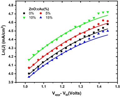 | ||
| Fig. 6 J–V characteristics of electron-only devices with the configuration of ITO/ZnO and ZnO:cAu NPs/active layer/LiF/Al. | ||
| ZnO:cAu (%) | μ0 (cm2 V−1 s−1) × 10−4 | σ (S m−1) × 10−5 |
|---|---|---|
| 0 | 0.92 | 0.96 |
| 5 | 0.95 | 1.12 |
| 10 | 1.04 | 1.17 |
| 15 | 0.86 | 1.13 |
3.6 Charge recombination kinetics
Further understanding of the reasons behind the improved JSC and FF can be obtained by looking closely into the charge recombination kinetics in the device. In this regard, the intensity-dependent JSC and VOC of the reference and optimized plasmonic device were recorded and analyzed as shown in Fig. 8(a) and (b) respectively. The JSC follows a power law dependence on light intensity i.e., JSC ∝ Pα where P is the intensity of incident light and α is an exponential factor acquired by fitting the slope of the JSC vs. P from double logarithmic plot.55 At short circuit conditions, the bimolecular recombination is minimal to sweep out all the generated charge carriers and get maximum current. Therefore, the deviation of α from 1 shows that bimolecular recombination of charge carriers is present in the devices. The calculated α values of the reference and device with ZnO:cAu NPs (10%) ETL were 0.931 and 0.972 respectively, confirming a weak bimolecular recombination in the optimized plasmonic OSCs (Fig. 8(a)). The lower bimolecular recombination in the optimized plasmonic OSCs is consistent with its highest collection efficiency and FF. Since the entire charge carrier generated in OSC recombine at the open circuit condition of a device, VOC is highly sensitive to the recombination kinetics of the devices Fig. 8(b). The slope of VOC versus ln(P) is given as nkT/q, where k, T, and q corresponds to the Boltzmann constant, temperature, and elementary charge, respectively.56 The value of n is between 1 and 2 where 1 and 2 represent the bimolecular-only and monomolecular-only recombination cases, respectively. The n values calculated for the devices made on reference ZnO and ZnO:cAu NPs (10%) ETL were 1.92 kT/q and 1.35 kT/q, respectively, indicating a highly trap-assisted recombination is a dominant charge carriers in the reference device's loss mechanism, while in the optimized plasmonic device bimolecular recombination is dominant over monomolecular recombination.57 This is consistent with the higher exciton quenching efficiency of the optimized plasmonic OSCs. The coarse morphology of pristine ZnO filled with defects could act as trap states that led to trap-assisted recombination in the reference devices.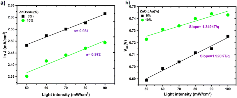 | ||
| Fig. 8 (a) Light intensity dependence of JSC and (b) VOC of devices without or with 10% cAu NPs in ZnO. | ||
4 Conclusions
To investigate the effect of cAu NP on the PCE of wide-band gap polymer-based devices, inverted OSCs based on PIDTT-DTBTz:PC71BM active layer with and without plasmonic cAu NPs embedded ZnO ETL were fabricated and investigated. The PCE of the reference device had been enhanced by more than 22% after the incorporation of 10 wt% cAu NPs in the ZnO layer, owing to higher JSC and FF. The device's JSC increased mostly due to better absorption in the active layer due to the LSPR of cAu NPs, which was found to promote exciton generation. Furthermore, the electromagnetic field surrounding the NPs was discovered to reduce exciton binding energy, improving exciton quenching in the active layer and thus assisting the charge photo-generation process, thus the JSC. When small-sized cAu NPs were embedded into the ZnO surface, the improved JSC and FF appeared to be related to the highly improved morphology of the ZnO layer. Moreover, when cAu NPs were embedded, the improved surface morphology increased the conductivity of the ETL from 0.96 × 10⁻⁵ to 1.17 × 10⁻⁵ S m−1, owing to reduced ZnO defects that act as traps. When compared to the reference device, the optimized plasmonic device's charge carrier mobility and charge collection efficiency increased from 9.20 × 10⁻⁵ to 1.04 × 10⁻⁴ (cm2 s−1 V−1) and 88.93 to 93.90%, respectively. In summary, it was established that embedding cAu NPs in the ZnO ETL layer of inverted OSCs based on PIDTT-DTBTz:PC71BM active layer increased the PCE of the reference device due to the synergistic effect of increased absorption, improved charge generation and mobility, and reduced bi-molecular recombination. Furthermore, when cAu NPs are embedded in ZnO, the device's stability is significantly improved when compared to the reference device. As a result, our work lays the door for a straightforward approach to improving both PCE and life-time of OSCs.Author contributions
AW did all the experimental work and drafted the manuscript CP, PN, GB, ZG, WM, EW synthesized and characterized the materials used in this work, FG and NT: conceptualization and supervision. All contributed to the editing of the manuscript.Conflicts of interest
There are no conflicts to declare.Acknowledgements
This work is based on the support from Organization for Women in Science for the developing world (OWSD), Trieste, Italy. We would also like to acknowledge the International Science Program (ISP), Uppsala University, Sweden for providing the laboratory facilities of the polymer physics laboratory in the Department of Physics of Addis Ababa University. ZG and WM would also like to acknowledge ISP for their financial support. African Laser Center is also acknowledged for funding part of this project, (HLHA23X Task ALC-R002).Notes and references
- Y. Lin, Y. Firdaus, F. H. Isikgor, M. I. Nugraha, E. Yengel, G. T. Harrison, R. Hallani, A. El-Labban, H. Faber and C. Ma, et al., ACS Energy Lett., 2020, 5, 2935–2944 CrossRef CAS
.
- W. Gao, F. Qi, Z. Peng, F. R. Lin, K. Jiang, C. Zhong, W. Kaminsky, Z. Guan, C.-S. Lee and T. J. Marks, et al., Adv. Mater., 2022, 34, 2202089 CrossRef CAS PubMed
.
- J. Wang, Y. Cui, Y. Xu, K. Xian, P. Bi, Z. Chen, K. Zhou, L. Ma, T. Zhang and Y. Yang, et al., Adv. Mater., 2022, 34, 2205009 CrossRef CAS PubMed
.
- F. Liu, L. Zhou, W. Liu, Z. Zhou, Q. Yue, W. Zheng, R. Sun, W. Liu, S. Xu and H. Fan, et al., Adv. Mater., 2021, 33, 2100830 CrossRef CAS PubMed
.
- S.-W. Baek, J. Noh, C.-H. Lee, B. Kim, M.-K. Seo and J.-Y. Lee, Sci. Rep., 2013, 3, 1726 CrossRef
.
- Q. N. Tran, J. H. Kim and S. J. Park, Mol. Cryst. Liq. Cryst., 2017, 645, 151–159 CrossRef CAS
.
- H. I. Park, S. Lee, J. M. Lee, S. A. Nam, T. Jeon, S. W. Han and S. O. Kim, ACS Nano, 2014, 8, 10305–10312 CrossRef CAS PubMed
.
- D. D. Fung, L. Qiao, W. C. Choy, C. Wang, E. Wei, F. Xie and S. He, J. Mater. Chem., 2011, 21, 16349–16356 RSC
.
- X. Gao, L. Yan, R. Xu and X. Sun, J. Mater. Sci.: Mater. Electron., 2018, 29, 19976–19984 CrossRef CAS
.
- M. Chalh, S. Vedraine, B. Lucas and B. Ratier, Sol. Energy Mater. Sol. Cells, 2016, 152, 34–41 CrossRef CAS
.
- C.-L. Huang, G. Kumar, G. D. Sharma and F.-C. Chen, Appl. Phys. Lett., 2020, 116, 253302 CrossRef CAS
.
- R. S. Ikhsanov, I. Protsenko and A. Uskov, Tech. Phys. Lett., 2013, 39, 450–453 CrossRef CAS
.
- A. G. Waketola, F. G. Hone, G. T. Mola, S. O. Oseni, H. Ogutu and N. A. Tegegne, Appl. Phys. A, 2023, 129, 96 CrossRef CAS
.
- E. Stratakis and E. Kymakis, Mater. Today, 2013, 16, 133–146 CrossRef CAS
.
- Y. H. Jang, Y. J. Jang, S. Kim, L. N. Quan, K. Chung and D. H. Kim, Chem. Rev., 2016, 116, 14982–15034 CrossRef CAS PubMed
.
- S.-W. Baek, J. Hun Kim, J. Kang, H. Lee, J. Young Park and J.-Y. Lee, Adv. Energy Mater., 2015, 5, 1501393 CrossRef
.
- C.-H. Kim, S.-H. Cha, S. C. Kim, M. Song, J. Lee, W. S. Shin, S.-J. Moon, J. H. Bahng, N. A. Kotov and S.-H. Jin, ACS Nano, 2011, 5, 3319–3325 CrossRef CAS PubMed
.
- H. Kaçuş, A. Baltakesmez, Z. Çaldıran, Ş. Aydoğan, M. Yılmaz and M. Sevim, Mater. Today: Proc., 2021, 46, 6986–6990 Search PubMed
.
- H. Kurt, Opt. Mater., 2022, 133, 113006 CrossRef CAS
.
- C.-P. Chen, I.-C. Lee, Y.-Y. Tsai, C.-L. Huang, Y.-C. Chen and G.-W. Huang, Org. Electron., 2018, 62, 95–101 CrossRef CAS
.
- Z. Liang, Q. Zhang, L. Jiang and G. Cao, Energy Environ. Sci., 2015, 8, 3442–3476 RSC
.
- C. Liu, C. Xiao and W. Li, J. Mater. Chem. C, 2021, 9, 14093–14114 RSC
.
- A. Purohit, S. Chander, A. Sharma, S. Nehra and M. Dhaka, Opt. Mater., 2015, 49, 51–58 CrossRef CAS
.
- A. Janotti and C. G. Van de Walle, Rep. Prog. Phys., 2009, 72, 126501 CrossRef
.
- A. Janotti and C. G. Van de Walle, Phys. Rev. B: Condens. Matter Mater. Phys., 2007, 76, 165202 CrossRef
.
- S. Li, Z. Li, X. Zhang, Z. Zhang, C. Liu, L. Shen, W. Guo and S. Ruan, Phys. Chem. Chem. Phys., 2016, 18, 24285–24289 RSC
.
- S. Liu, Y. Sun, L. Chen, Q. Zhang, X. Li and J. Shuai, Mater. Today Phys., 2022, 100680 CrossRef CAS
.
- B. Usmani, R. Ranjan, Prateek, S. K. Gupta, R. K. Gupta, K. S. Nalwa and A. Garg, Sol. Energy, 2021, 214, 220–230 CrossRef CAS
.
- N. Chaturvedi, S. K. Swami and V. Dutta, Nanoscale, 2014, 6, 10772–10778 RSC
.
- J. Rivera-Taco, R. Castro-Beltrán, J.-L. Maldonado, J. Álvarez-Martínez, D. Barreiro-Argüelles, J. A. Gaspar and G. Gutiérrez-Juárez, J. Electron. Mater., 2021, 50, 4118–4127 CrossRef CAS
.
- H. Kaçuş, Ş. Aydoğan, M. Biber, Ö. Metin and M. Sevim, Mater. Res. Express, 2019, 6, 095104 CrossRef
.
- Y. Lin, H. Fan, Y. Li and X. Zhan, Adv. Mater., 2012, 24, 3087–3106 CrossRef CAS PubMed
.
- B. Guo, W. Li, X. Guo, X. Meng, W. Ma, M. Zhang and Y. Li, Nano Energy, 2017, 34, 556–561 CrossRef CAS
.
- A. Negash, Z. Genene, R. T. Eachambadi, P. Verstappen, N. Van den Brande, J. Kesters, J. D'Haen, E. Wang, K. Vandewal and W. Maes, et al., Org. Electron., 2019, 74, 211–217 CrossRef CAS
.
- Y. Q. He, S. P. Liu, L. Kong and Z. F. Liu, Spectrochim. Acta, Part A, 2005, 61, 2861–2866 CrossRef PubMed
.
- Y. Sun, J. H. Seo, C. J. Takacs, J. Seifter and A. J. Heeger, Adv. Mater., 2011, 23, 1679–1683 CrossRef CAS PubMed
.
- J. Tan, B. Hao, C. Wang, Y. Ren, H. Hao and R. Yang, et al., J. Forensic Sci. Med., 2016, 2, 195 CrossRef
.
- J. Liu, H. He, D. Xiao, S. Yin, W. Ji, S. Jiang, D. Luo, B. Wang and Y. Liu, Materials, 2018, 11, 1833 CrossRef PubMed
.
- X. Zhao, M. Li, L. Jiang, H. Tang and Y. Guan, Front. Chem., 2021, 9, 683728 CrossRef CAS PubMed
.
- J. Li, M. Ren, J. Qing, Y. Wang, Z. Liang, N. Wang, J. Tong, C. Yang and Y. Xia, Mol. Cryst. Liq. Cryst., 2019, 692, 74–82 CrossRef
.
- E. Ramya, M. V. Rao, L. Jyothi and D. N. Rao, J. Nanosci. Nanotechnol., 2018, 18, 7072–7077 CrossRef CAS PubMed
.
- C. Hou and H. Yu, Chem. Eng. J., 2021, 407, 127192 CrossRef CAS
.
- J. Huang, H. Yu and X. Zhou, Chem. Eng. J., 2022, 428, 131366 CrossRef CAS
.
- F. Ruske, M. Roczen, K. Lee, M. Wimmer, S. Gall, J. Hüpkes, D. Hrunski and B. Rech, J. Appl. Phys., 2010, 107, 013708 CrossRef
.
- J. R. Lakowicz, Anal. Biochem., 2005, 337, 171–194 CrossRef CAS PubMed
.
- W. M. Dlamini, PhD thesis, University of KwaZulu-Natal, 2022
.
- X. Huang, H. Yu, S. Shi and C. Huang, Org. Electron., 2019, 65, 311–320 CrossRef CAS
.
- Y. Xu, H. Zhou, P. Duan, B. Shan, W. Xu, J. Wang, M. Liu, F. Zhang and Q. Sun, Molecules, 2022, 27, 6363 CrossRef CAS PubMed
.
- M. Li, J. Li, L. Yu, Y. Zhang, Y. Dai, R. Chen and W. Huang, Front. Chem., 2020, 8, 399 CrossRef CAS PubMed
.
- M. Wang, J. Li, X. Ma, J. Lv, C. Zhang and Y. Xia, Polym. Adv. Technol., 2018, 29, 914–920 CrossRef CAS
.
- V. Mihailetchi, J. Wildeman and P. Blom, Phys. Rev. Lett., 2005, 94, 126602 CrossRef CAS PubMed
.
- H. Hwang, D. H. Sin, C. Park and K. Cho, Sci. Rep., 2019, 9, 12081 CrossRef PubMed
.
- T. Yan, W. Song, J. Huang, R. Peng, L. Huang and Z. Ge, Adv. Mater., 2019, 31, 1902210 CrossRef PubMed
.
- J. N. Ike, M. W. Dlamini, R. P. Dwivedi, Y. Zhang and G. T. Mola, J. Phys. Chem. Solids, 2022, 165, 110662 CrossRef CAS
.
- R. Sharma, N. Jain, H. Lee, D. Kabra and S. Yoo, ACS Appl. Mater. Interfaces, 2020, 12, 45083–45091 CrossRef CAS PubMed
.
- S. Wheeler, F. Deledalle, N. Tokmoldin, T. Kirchartz, J. Nelson and J. R. Durrant, Phys. Rev. Appl., 2015, 4, 024020 CrossRef
.
- T. Kong, R. Wang, D. Zheng and J. Yu, Front. Chem., 2021, 9, 703561 CrossRef CAS PubMed
.
Footnote |
| † Electronic supplementary information (ESI) available: The absorbance and PL spectra of ZnO:cAu (%) ETLs, electric field dependent PL of PIDTT-DTBTz/ZnO:cAu (%) and J–V curves under dark condition of the OSCs is given in the ESI. See DOI: https://doi.org/10.1039/d3ra01078c |
| This journal is © The Royal Society of Chemistry 2023 |


