
 Open Access Article
 This Open Access Article is licensed under a Creative Commons Attribution-Non Commercial 3.0 Unported Licence
Influence of external electric field on electronic structure and optical properties of β-Ga2O3: a DFT study
Hao Wu a,
Cuihua Zhao*ab,
WenBo Zhaoa,
Linji Lia and
Chengcheng Zhanga
a,
Cuihua Zhao*ab,
WenBo Zhaoa,
Linji Lia and
Chengcheng Zhanga
aSchool of Resources, Environment and Materials, Guangxi University, Nanning 530004, China. E-mail: chzhao@gxu.edu.cn
bState Key Laboratory of Featured Metal Materials and Life-cycle Safety for Composite Structures, Guangxi University, Nanning 530004, China
First published on 15th September 2023
Abstract
The influence of different electric fields on the electronic structure and optical properties of β-Ga2O3 was studied by GGA+U method. The results show that appropriate electric field intensity can regulate the band gap of β-Ga2O3 more effectively to improve the photoelectric characteristics. The band gap value of intrinsic β-Ga2O3 is 4.865 eV, and decreases from 4.732 to 2.757 eV with the increase of electric field intensity from 0.05 to 0.20 eV Å−1. The length of the O–Ga bond along the electric field increases the fastest with the electric field intensity, and the distance between O and Ga reaches 2.52 Å when the electric field intensity is 0.20 eV Å−1. A new peak appears in the real and imaginary parts of the dielectric function for β-Ga2O3 in the low frequency region under the electric field, and the conductivity increases obviously. The optical absorption peaks induced by the electric field were observed in the wavelength range of 400–600 nm. The optical absorption of β-Ga2O3 is enhanced with an increase of electric field intensity, exhibiting a maximum value with the electric field of 0.15 eV Å−1. The electric field above 0.15 eV Å−1 causes a decrease of optical absorption intensity.
1. Introduction
Ga2O3, a fourth-generation semiconductor, is a transparent and multi-crystalline (α, β, γ, δ, and ε) material with an ultra-wide band gap.1 Among them, β-Ga2O3 is the most stable at room temperature, and has received widespread attention in recent years.2 Currently, β-Ga2O3 films and nanostructures can be successfully prepared by a floating zone method, edge-defined film-fed growth process, metal–organic vapor homoepitaxy, and chemical vapor deposition.3–6 The band gap value of 4.9 eV measured experimentally7 corresponds to the ultraviolet (UV) light band, and is a natural solar-blind photoelectric detection material.8 β-Ga2O3 has a high breakdown field strength of 8 MeV cm−1 which is more than twice as high as third-generation semiconductors (GaN, SiC), and a Baliga's figure of merit (FOM – the basic parameter to show how suitable a material is for power devices) of 3444 that is one order of magnitude higher than those of GaN and SiC,9 which makes β-Ga2O3 the preferred material for current and future high-voltage resistant and low-loss power devices. Due to the amazing physical properties, and good electronic and optical properties, β-Ga2O3 shows great potential in various fields. Hu et al. reported a Schottky barrier diode based on β-Ga2O3, which achieves a record reverse blocking voltage of over 3 kV and a DC power figure of merit of 500 MW cm−2.10 In decomposing water/alcohol mixtures, Navarrete et al. compounded TiO2 with Ga2O3, and detected excellent hydrogen-producing activity under UV light.11 Zhao et al. constructed a self-powered solar-blind photodetector based on a single ZnO–Ga2O3 core–shell heterostructure, which achieves an ultra-high responsivity of 9.7 mA W−1 at 251 nm.12 In addition, due to the dual lithium storage mechanism of conversion and alloying reactions and the self-healing capability of the cycling process, gallium-based materials (Ga2O3, GaN) are even expected to become high-performance anodes for alkali metal (Li, Na, K) ion batteries in the future.13 In the last decade, Ga2O3 anodes with high capacity and high cycling characteristics have been continuously prepared, such as nanoparticles, nanohollow spheres, nanorods, nanosheets, MOF dodecahedra etc.14–19Although the current performance of Ga2O3 in the above mentioned fields is satisfactory, there are still some problems to be solved: (1) the intrinsic ultra-wide band gap leads to lower carrier mobility, implying low conductivity, which almost affects the application of β-Ga2O3 in all fields.20 (2) The maximum absorption edge of 260 nm has been measured experimentally.21 Even though it exhibits extremely high light absorption in the UV band, the utilization rate of visible light is almost zero, while visible light is readily available and more environmentally friendly. (3) So far, β-Ga2O3 can easily achieve n-type doping, but actual effective p-type doping remains difficult.22,23 (4) Volume expansion during battery charging and discharging is a nightmare for all anodes. Although the inherent liquidization of gallium groups mitigates the volume effect, its intrinsic reaction mechanism is still not understood.24,25
Due to these shortcomings, the application of Ga2O3 is greatly limited, especially in the utilization of visible light in photocatalysis. Study has shown that a suitable electric fields can tune the band gap of the semiconductors, thereby changing their optical absorption range. Also it is much easier to control the electric field experimentally compared to other methods. Kang et al. reported the modulating effect of transverse electric field on the band gap of graphdiyne nanoribbons, where the band gap decreased and a semiconductor–metal transition occurred with increasing field strength.26 Feng et al. used a vertical electric field to modulate the band gap and carrier mobility of SiAs2/GeAs2 in-plane lateral heterostructures, and the mobility of holes and anisotropy changed significantly.27
Previously, most of the research on β-Ga2O3 has focused on doping modification,28–30 but there is relatively little research on the regulation of its optical properties by electric field. As is well known, the property of a semiconductor depends on its electronic structure.31–33 In this paper, we study by using DFT method the change of electronic structure for β-Ga2O3 under different electric fields, and explore the regulation of electric fields on the band gap of β-Ga2O3, and develop an effective way to apply β-Ga2O3 to the field of photocatalysis using sunlight. In addition, we also studied the influence of different intensities of electric field on the optical properties of β-Ga2O3. This study can save manpower, material resources, and financial resources, and provide a theoretical guidance for its experimental research and industrial applications.
2. Computational models and methods
β-Ga2O3 possesses a monoclinic crystal structure with a space group of C2/m. Each cell contains 8 gallium atoms and 12 oxygen atoms, as shown in Fig. 1. The lattice parameters of optimized β-Ga2O3 are a = 12.445 Å, b = 3.075 Å, c = 5.852 Å, and β = 103.736°, with a maximum deviation of no more than 1.76% from the experimental measurements,34 which indicates that the calculation is reliable.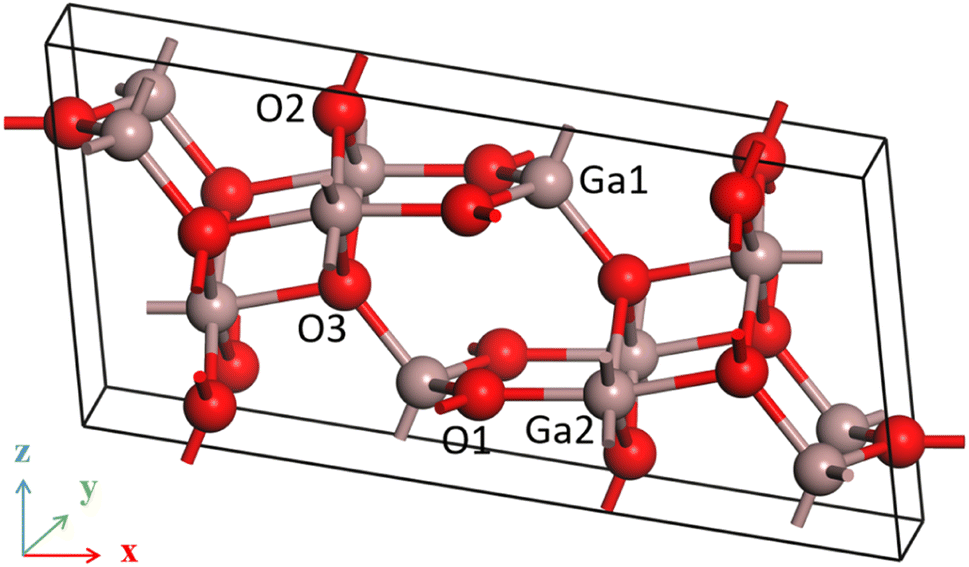 | ||
| Fig. 1 Model of β-Ga2O3. | ||
All calculations in this paper were performed using the Cambridge Serial Total Energy Package (CASTP module) in Material Studio 2017. In CASTEP module, the parameters of the electric field can be set, including the different directions (X, Y and Z) and intensities. The simulation algorithm for the UV-Vis spectra is based on standard DFT Kohn–Sham orbitals. Electron exchange and correlation effects were treated using the PW91 generalized function in the generalized gradient approximation GGA. The ultra soft pseudopotential was used to describe the interaction between valence electrons and ion nuclei, and the valence electron configurations of Ga and O are 3d104s24p1 and 2s22p4, respectively. The generalized gradient approximation of GGA tends to underestimate the band gap, and corrections are generally made using GGA+U and scissor operators in order to obtain relatively accurate band gaps. Hubbard U is theoretically a correction for strongly correlated systems such as d and f orbital self-interactions for corrections. Many β-Ga2O3-related DFT studies set U values in both Ga 3d and O 2p orbitals to make the calculation results reliable.35–37 There are different opinions on the selection of U value. Some researchers thought that the value of U can be as high as 14.0 eV.37 However, others believed that too high U value (more than 5 eV) will affect the electric properties.38 Therefore, in this paper, the U values of the 3d orbitals of gallium and the 2p orbitals of oxygen were set to 5 eV and 3.5 eV, respectively. If the U value of 5 eV for Ga 3d and 3.5 for O 2p can not adjust the bandgap value to match the experimental value, the further adjustment can be made by using scissors. In the GGA algorithm, the scissors value itself is used as an operation method to correct the band gap underestimation. For the material with a known experimental bandgap value, the scissors operator is set to the difference between the experimental and calculated values. It can be expressed by the formula “scissors value = band gap (experimental value) − band gap (calculated value)”. The experimental band gap of beta-Ga2O3 is between 4.8–4.9 eV, and the calculated band gap without scissors value by GGA+U method is 3.315 eV. When the scissors value is 1.55 eV, the calculated bandgap value of beta-Ga2O3 is 4.865 eV, which is consistent with the experimental value. Therefore, a scissor value of 1.55 eV in this paper is introduced to compensate for the errors caused by DFT in GGA functional, which is insufficient to process inter-electron exchange interaction. In the calculation, the special K-point sampling in the integrable Brillouin zone was performed using a 1 × 4 × 2 grid for β-Ga2O3 singlet with a plane wave cut-off energy of 340 eV based on test results. The convergence tolerance of the geometry-optimized atomic step was set to a maximum displacement of 0.001 Å and a maximum stress of 0.05 GPa, the maximum energy change was less than 10−5 eV per atom, the self-consistent field ion step (SCF) was less than 10−6 eV per atom. In addition, the convergence tolerance of the maximum force was set to 0.03 eV Å−1 by testing results. The geometric optimization of beta-Ga2O3 is difficult to converge with the maximum force of 0.03 eV Å−1 or 0.02 eV Å−1 when the external electric field was applied, especially under large electric field intensity (0.2 eV Å−1). When the convergence criteria of geometry relaxation is 0.03 eV Å−1, the geometric structure of beta-Ga2O3 under the electric fields of 0.05 to 0.20 eV Å−1 can converge successfully. Therefore, setting 0.03 eV Å−1 as the convergence criteria of geometry relaxations is reliable.
The electronic structure and optical properties of β-Ga2O3 were calculated by using a scissors value of 1.55 eV. To ensure the accuracy of the calculation results, we studied the band structure, density of states, and absorption spectra of β-Ga2O3 before and after using scissors values. The results found the band gap value beta-Ga2O3 with a scissors value of 1.55 eV increases to 4.865 eV from 3.315 eV (without using scissors value), which is mainly due to the movement of the conduction band to the high energy. Similar to changes in band structure, DOS of the valence band is almost unaffected, while DOS curve of the conduction band shifts to high energy. As for optical absorption, the maximum absorption edge with a scissors value of 1.55 eV moves to high energy compared to that without scissors value, which is consistent with the maximum absorption edge of 260 nm measured experimentally. The result suggests that it is reasonable to use a scissors value of 1.55 eV.
3. Results and discussion
3.1 Geometry structure of β-Ga2O3 with different electric fields
In β-Ga2O3, O atoms have three and four coordination modes, and Ga atoms have four and six coordination modes. And, all coordination and bonding information of atoms are detailed in Table 1.| Atom species | Coordination number | Coordination atom | Type of bond |
|---|---|---|---|
| O1 | 3 | Two 4-coordinated Ga | Ga–O |
| 6-Coordinated Ga | Ga–O | ||
| O2 | 3 | 4-Coordinated Ga | Ga–O |
| Two 6-coordinated Ga | Ga–O | ||
| O3 | 4 | 4-Coordinated Ga | Ga–O |
| Three 6-coordinated Ga | Ga–O | ||
| Ga1 | 4 | Three 3-coordinated O | Ga–O |
| 4-Coordinated O | Ga–O | ||
| Ga2 | 6 | Three 3-coordinated O | Ga–O |
| Three 4-coordinated O | Ga–O |
It is seen that three coordination oxygen atoms have two types. In the first type (O1), one O–Ga bond (O1–Ga2) has a bond length of 1.97 Å, which is nearly parallel to x direction, and two equivalent O–Ga bonds (O1–Ga3 and O1–Ga4) have a bond length of 1.85 Å. In the second type (O2), lengths of one O–Ga bond with a small angle deviation from the vertical direction (O2–Ga4) is 1.85 Å, and that of two equivalent O–Ga bonds (O2–Ga5 and O2–Ga6) are 1.96 Å. Four coordination oxygen (O3) has one O–Ga bond with a bond length of 2.03 Å (O3–Ga7), one O–Ga bond with a bond length of 1.88 Å (O3–Ga8), and two equivalent O–Ga bonds with a bond length of 2.11 Å (O3–Ga5 and O3–Ga6). For four coordination gallium (Ga1), there are three O–Ga bonds with a bond length of 1.85 Å (O4–Ga1, O5–Ga1 and O7–Ga1) and one O–Ga bond with a bond length of 1.88 Å (O6–Ga1). As for six coordination gallium (Ga2), there are two equivalent O–Ga bonds with a bond length of 2.11 Å (O9–Ga2 and O10–Ga2), two equivalent O–Ga bonds with a bond length of 1.96 Å (O7–Ga2 and O8–Ga2), one O–Ga bond of 1.97 Å (O1–Ga2), and one O–Ga bond with a bond length of 2.03 Å (O11–Ga2). These information is shown in Fig. 2(a).
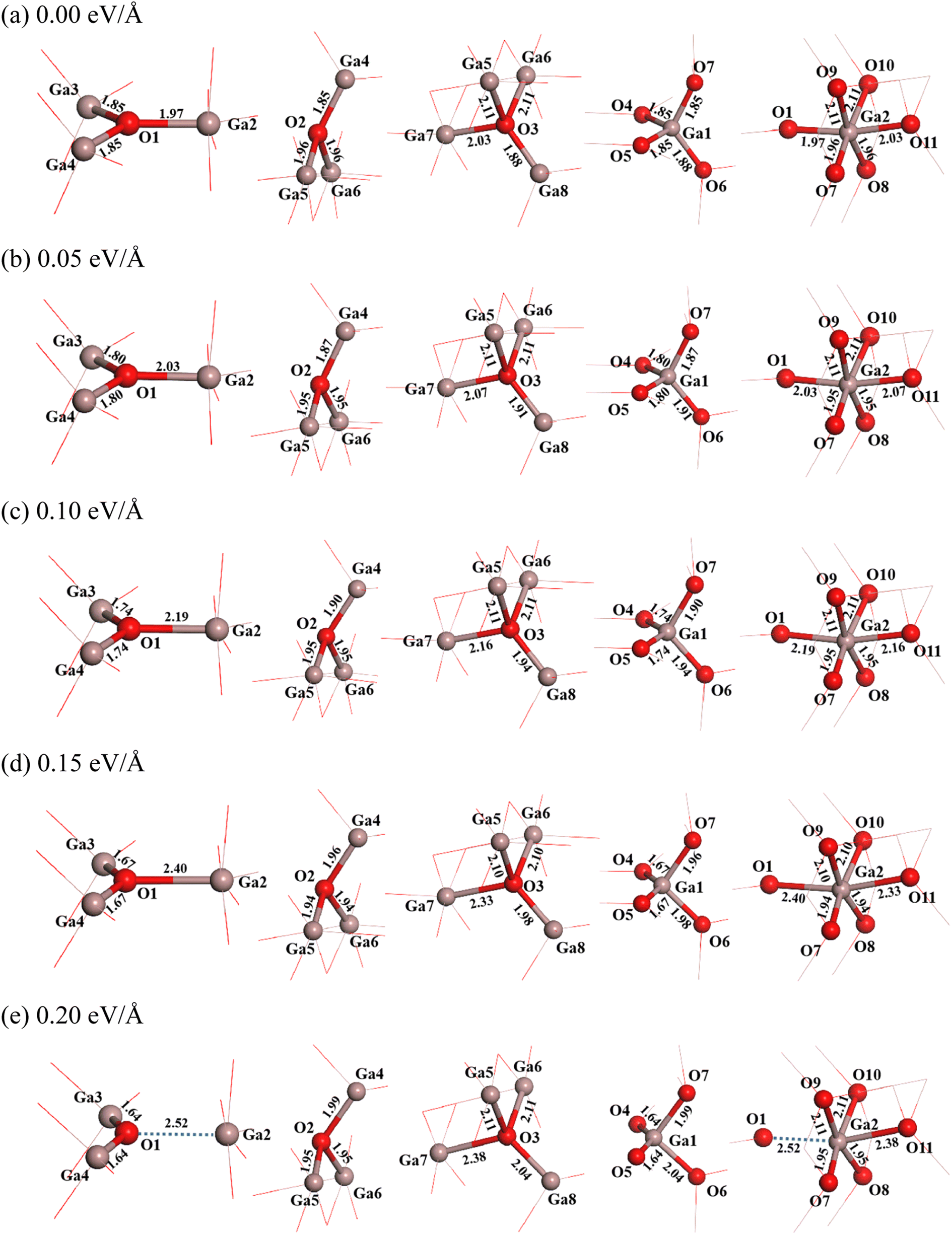 | ||
| Fig. 2 Structural changes of β-Ga2O3 under different electric fields of 0 eV Å−1 (a), 0.05 eV Å−1 (b), 0.10 eV Å−1 (c), 0.15 eV Å−1 (d) and 0.20 eV Å−1 (e). | ||
The influences of different electric field directions on the structure were studied, including x, y and z direction. According to the calculating results, it is found that the effect of electric field along x direction on the structure of β-Ga2O3 is larger compared to those of the other two directions. Therefore, we only discuss the structures and optical properties of β-Ga2O3 under the action of the electric field along x direction.
The most obvious change caused by electric field may be attributed to the Ga–O octahedral double chain structure in β-Ga2O3. The double chains are connected each other by Ga–O tetrahedral angles, which leads to a cleavage surface in the (100) direction of β-Ga2O3. Also, the (100) direction possesses a larger lattice constant compared to other directions, so it was found that β-Ga2O3 films of nanometer thickness can be easily mechanically exfoliated from bulk crystals.39 Therefore, we only discuss the structures and properties of β-Ga2O3 under the action of the electric field along x direction. Fig. 2(b)–(e) shows the structural change of β-Ga2O3 with the electric field of 0.05 eV Å−1, 0.10 eV Å−1, 0.15 eV Å−1 and 0.20 eV Å−1.
It is found that the structure of β-Ga2O3 undergoes significant changes after applying an electric field. When the electric field intensity is 0.05 eV Å−1, in the three-coordination structure of O1, the length of O1–Ga2 bond almost parallel to the direction of the electric field increases from 1.97 Å to 2.03 Å, and those of other two bonds (O1–Ga3 and O1–Ga4) decrease from 1.85 Å to 1.80 Å. The length of O1–Ga2 bond increases further with the increase of electric field intensity from 0.05 eV Å−1 to 0.15 eV Å−1. When the intensity of electric field is 0.20 eV Å−1, the lengths of O1–Ga3 and O1–Ga4 bonds decrease further to 1.64 Å, while the distance between O1 and Ga2 is increased to 2.52 Å. This may be due to the fact that the O1–Ga2 bond is almost parallel to the direction of the electric field, and is exactly perpendicular to the cleavage plane (100) of β-Ga2O3. The three-coordination structure of O2 changes little when applying weak electric field (0.05 eV Å−1), the length of O2–Ga4 bond is slightly increases from 1.85 Å to 1.87 Å, and those of O2–Ga5 and O2–Ga6 bonds slightly decrease from 1.96 Å to 1.95 Å. With further increasing the electric field intensity from 0.05 eV Å−1 to 0.20 eV Å−1, the length of O2–Ga4 bond increases from 1.87 Å to 1.99 Å, while those of O2–Ga5 and O2–Ga6 bonds have no change. For the four-coordination structure of O3, the lengths of O3–Ga5 and O3–Ga6 bonds which are almost perpendicular to the electric field are constant when applying a weak electric field (0.05 eV Å−1), while those of other two bonds increase. The length of O3–Ga7 bond, which is almost parallel to the direction of the electric field, increases from 2.03 Å to 2.07 Å, and that of O3–Ga8 bond increases slightly from 1.88 Å to 1.91 Å. With further increasing the electric field intensity from 0.05 eV Å−1 to 0.20 eV Å−1, the lengths of O3–Ga5 and O3–Ga6 bonds still have no change, while that of O3–Ga7 increases from 2.07 Å to 2.38 Å, and that of O3–Ga8 bond increases from 1.91 Å to 2.04 Å.
For the four coordination structure of Ga1, the lengths of O4–Ga1 and O5–Ga1 bonds decrease from 1.85 Å to 1.80 Å when applying a weak electric field (0.05 eV Å−1), and the lengths of O6–Ga1 and O7–Ga1 bonds increase slightly. The length of O6–Ga1 increases from 1.88 Å to 1.91 Å, and that of O7–Ga1 bond increases from 1.85 Å to 1.87 Å. With further increasing the electric field intensity from 0.05 eV Å−1 to 0.20 eV Å−1, the lengths of O4–Ga1 and O5–Ga1 bonds decrease from 1.80 Å to 1.64 Å, while the length of O6–Ga1 bond increases from 1.91 Å to 2.04 Å, and that of O7–Ga1 bond increases from 1.87 Å to 1.99 Å. As for the 6-coordination structure of Ga2, it is found that the four O-Ga2 bonds (O7–Ga2, O8–Ga2, O9–Ga2 and O10–Ga2) that are nearly perpendicular to the electric field almost have no change in bond length when applying the electric field. The lengths of O7–Ga2 and O8–Ga2 bonds remain about 1.95 Å, while those of O9–Ga2 and O10–Ga2 bonds remain about 2.11 Å. However, the bond lengths of O1–Ga2 and O11–Ga2 along the electric field direction increase. The length of O11–Ga2 bond increases from 2.03 Å to 2.38 Å with an increase of the electric field intensity from 0 eV Å−1 to 0.20 eV Å−1. The change of O1–Ga2 bond with the electric field intensity has been described, which increases with the increase of electric field intensity, and the distance between O1 and Ga2 reaches to 2.52 Å when the electric field intensity increases to 0.20 eV Å−1.
3.2 Band structure and density of states of β-Ga2O3
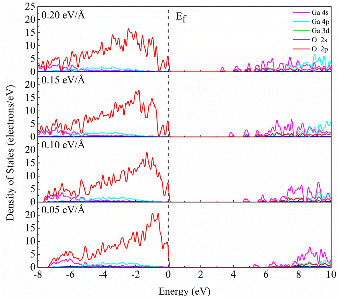
Fig. 3 shows the band structure and density of states distribution of the initial β-Ga2O3, setting the Fermi energy level to 0 eV. The electron distribution near the Fermi energy level is more meaningful for practical studies, so the PDOS maps in the range of −8 to 10 eV are taken for control analysis. It is found that the conduction band minimum (CBM) is mainly occupied by the electrons of Ga 4s orbital. The main contribution of the conduction band is from 4s state of Ga with small contribution from Ga 4p, O 2p and O 2s. The valence band maximum (VBM) near the Fermi energy level is occupied mainly by the electrons of O 2p orbital. The main contribution of the valence band is from 2p state of O with small contribution from Ga 4p, Ga 4s and O 2s. The energy band and PDOS diagrams together describe the distribution of the energy levels occupied by the internal electrons, and the band gap values are closely related to the electrical conductivity and light absorption of the material. The calculated intrinsic band gap value of 4.865 eV for β-Ga2O3 without the electric field is in agreement with the experimental value, which corresponds to the UV light absorption and low conductivity of β-Ga2O3. In addition, the entire valence band below the Fermi energy level consists of almost O 2p states, making the valence band very flat and crowded, resulting in a large effective mass of holes of β-Ga2O3. Almost all wide band gap oxide semiconductors have the same low dispersion valence band formed by O 2p, and thus there is a prevalent internal hole self-trapping effect.40 This greatly limits the hole migration, and is one of the reasons why β-Ga2O3 is difficult to achieve p-type semiconductors.41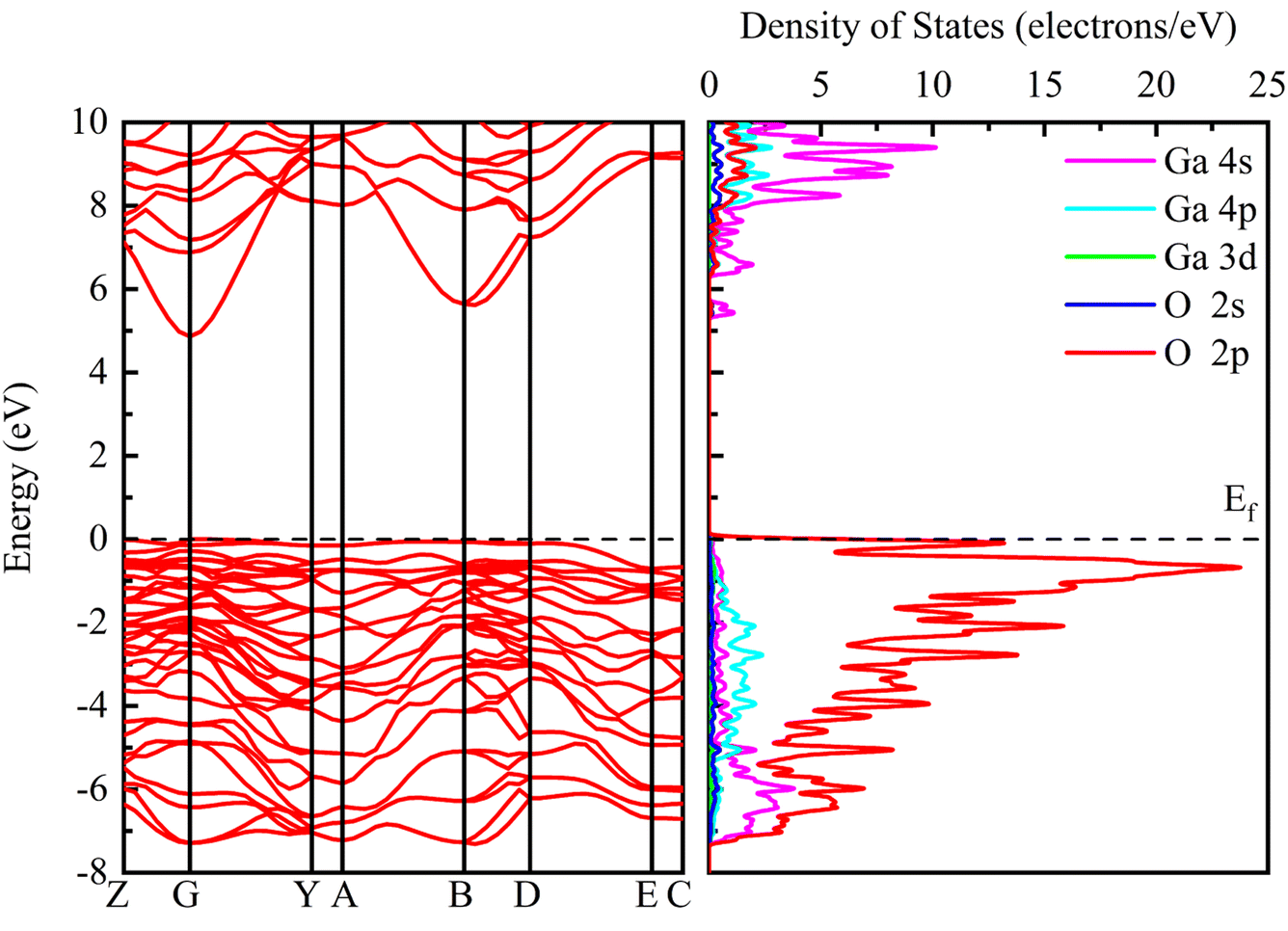 | ||
| Fig. 3 Band structure and PDOS of initial β-Ga2O3 without electric field. | ||
The energy band structures with different electric field strengths are shown in Fig. 4. It is observed that the bottom of the conduction band gradually shifts to Fermi level, and the band gap decreases significantly with the increasing the electric field intensity. When the electric field increases from 0 eV Å−1 to 0.20 eV Å−1, the band gap value decreases from the initial 4.865 eV to 2.757 eV. However, β-Ga2O3 is still a semiconductor and does not undergo a transition to metal. The decrease of the band gap can be explained by a giant Stark effect, i.e., the redistribution of the wave function in the presence of an external electric field.26,42
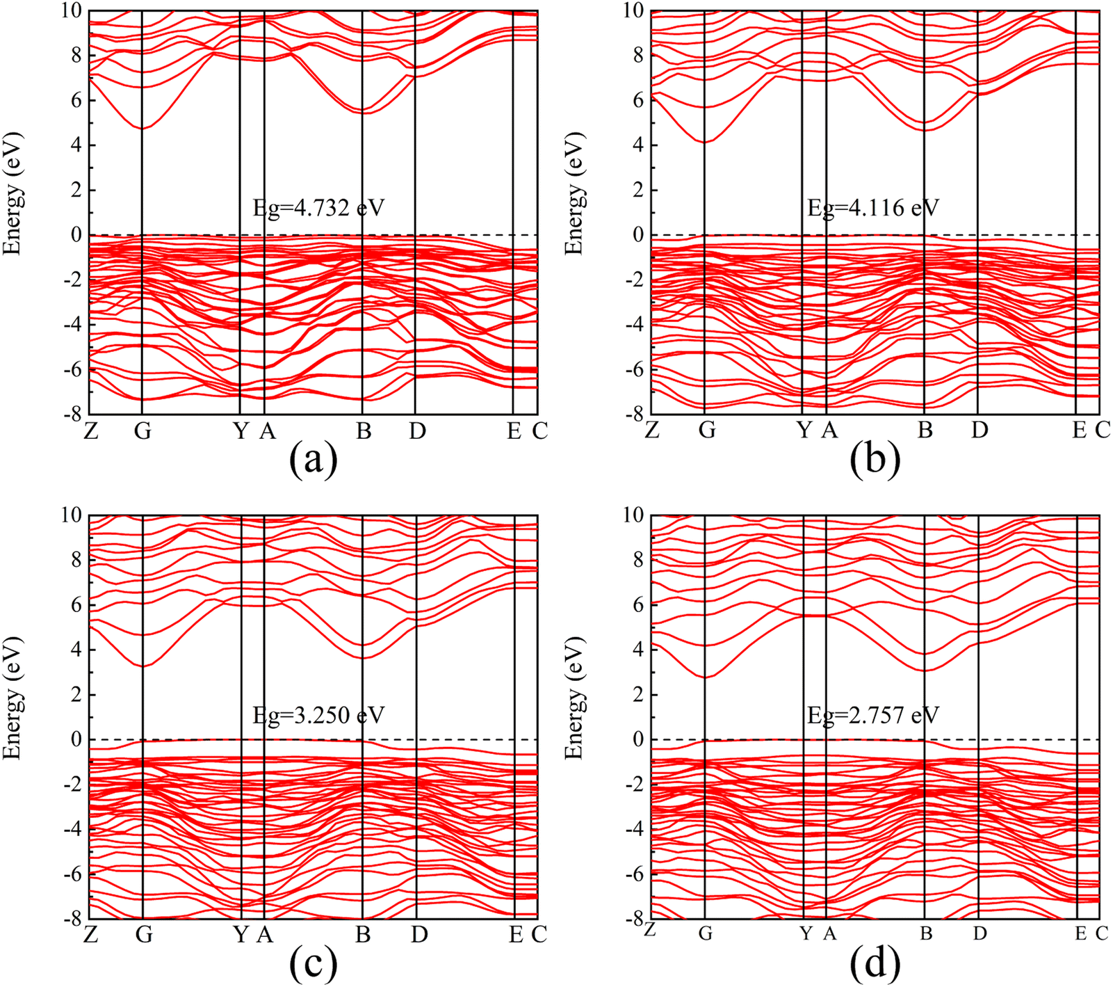 | ||
| Fig. 4 Band structure of β-Ga2O3 with different electric fields. (a) 0.05 eV Å−1, (b) 0.10 eV Å−1, (c) 0.15 eV Å−1, (d) 0.20 eV Å−1. | ||
Fig. 5 shows the partial density of states of β-Ga2O3 with different electric field intensities. It is obvious that DOS curve of β-Ga2O3 in the conduction band shifts to Fermi level with the increase of the electric field intensity, which leads to the decrease of the band gap. In addition, it is also found that the DOS of Ga 4p in the conduction band increases with increasing the electric field intensity. DOS curve of β-Ga2O3 in the valence band extends toward low energy with the increase of electric field intensity. DOS peaks of all orbitals become wider due to the slight dispersion of the valence band. The dispersion of the valence band alleviates the self-trapping of the internal holes to some extent, but the valence band composition of the O 2p state remains the main factor inducing the self-trapping. Small peaks formed by splitting the DOS curve of O 2p become more sharp with the increase of electric field intensity form 0.05 eV Å−1 to 0.10 eV Å−1. When the electric field intensity increases to 0.15 eV Å−1, DOS curve of O 2p near Fermi level is split into two small peaks. However, DOS of small peak decreases with increasing the electric field intensity from 0.05 eV Å−1 to 0.15 eV Å−1. Two small peaks with the electric field intensity of 0.20 eV Å−1 is similar with that with electric field intensity of 0.15 eV Å−1. In addition, it is also observed that the localization of DOS peak for O 2p in the valence band gradually decreases with an increase of electric field intensity.
 | ||
| Fig. 5 PDOS analysis of β-Ga2O3 with different electric fields. | ||
3.3 Mulliken charge populations and electron density difference
Table 2 shows the Mulliken atomic populations of O1, O2, O3, Ga1 and Ga2 atoms. It is observed all O atoms gain electrons with the negative charges, and all Ga atoms lose electrons with the positive charges. With the increase of electric field intensity, the charges of all five atoms have undergone significant changes. It is seen that the negative charge of O1 atom increases from −0.96 to −1.02e when the electric field intensity increases from 0 eV Å−1 to 0.20 eV Å−1, which is attributed mainly to the increase of its 2p orbital electrons with a small change of its 2s orbital electrons. On the contrary, the negative charge of O2 atom gradually decreases from −0.95 to −0.89e with increasing the electric field intensity from 0 eV Å−1 to 0.20 eV Å−1, which is mainly due to the decrease of its 2p orbital electrons with a small change of its 2s orbital electrons. The trend of charge change of O3 is the similar to that of O2. Its negative charge decreases with an increase of the electric field intensity, and the charge is close to that of O2 when electric field intensity is 0.20 eV Å−1 (O2: −0.89e; O3: −0.90e). For Ga1, the positive charge remains unchanged with low electric field intensity (0.05 eV Å−1 and 0.10 eV Å−1). When the electric field intensity exceeds 0.15 eV Å−1, its positive charge slightly decreases, which is attributed mainly to the increase of 4s orbital electrons of Ga1 atom. As for Ga2, it is found that the positive charge hardly changes with the electric field intensity, which may be due to its high symmetry along the electric field direction.| Atomic label | Electric field | s | p | d | Charge (e) |
|---|---|---|---|---|---|
| O1 | 0.00 | 1.83 | 5.13 | −0.96 | |
| 0.05 | 1.83 | 5.14 | −0.97 | ||
| 0.10 | 1.82 | 5.17 | −0.98 | ||
| 0.15 | 1.81 | 5.20 | −1.01 | ||
| 0.20 | 1.80 | 5.22 | −1.02 | ||
| O2 | 0.00 | 1.84 | 5.11 | −0.95 | |
| 0.05 | 1.84 | 5.10 | −0.95 | ||
| 0.10 | 1.85 | 5.08 | −0.93 | ||
| 0.15 | 1.87 | 5.05 | −0.91 | ||
| 0.20 | 1.87 | 5.02 | −0.89 | ||
| O3 | 0.00 | 1.85 | 5.07 | −0.93 | |
| 0.05 | 1.86 | 5.07 | −0.92 | ||
| 0.10 | 1.86 | 5.05 | −0.92 | ||
| 0.15 | 1.87 | 5.03 | −0.91 | ||
| 0.20 | 1.88 | 5.02 | −0.90 | ||
| Ga1 | 0.00 | 0.55 | 1.00 | 10.00 | 1.46 |
| 0.05 | 0.55 | 0.99 | 10.00 | 1.46 | |
| 0.10 | 0.56 | 0.99 | 9.99 | 1.46 | |
| 0.15 | 0.58 | 0.99 | 9.99 | 1.44 | |
| 0.20 | 0.60 | 0.98 | 9.99 | 1.42 | |
| Ga2 | 0.00 | 0.64 | 0.99 | 10.00 | 1.38 |
| 0.05 | 0.63 | 0.99 | 10.00 | 1.38 | |
| 0.10 | 0.64 | 0.99 | 10.00 | 1.38 | |
| 0.15 | 0.64 | 0.98 | 10.00 | 1.39 | |
| 0.20 | 0.64 | 0.98 | 10.00 | 1.38 |
The charge transfer can also be represented by an electron density difference plot. Here we compare the charge distribution of atoms in β-Ga2O3 under the action of 0 eV Å−1 and 0.15 eV Å−1 (Fig. 6). The blue region indicates electron loss, while the red region indicates electron enrichment. It is observed that the electron density around O1 atom with the electric field of 0.15 eV Å−1 significantly increases compared to that of 0 eV Å−1, while those around O2 and O3 slightly decreases, and the electron density around Ga1 and Ga2 with the electric field of 0.15 eV Å−1 increases, which were proved by the difference of charge density of β-Ga2O3 atoms between the electric field of 0.15 eV Å−1 and 0 eV Å−1 (Table 3). The difference of charge density of O1 is 0.06, while those of O2 and O3 are −0.04 and −0.03, respectively. Besides that, the difference of charge density of Ga1 and Ga2 are 0.07 and 0.09, respectively. These results are also in agreement with those of Mulliken analysis.
 | ||
| Fig. 6 Electron density difference of β-Ga2O3 under electric fields. (a) 0 eV Å−1, (b) 0.15 eV Å−1. | ||
| O1 | O2 | O3 | Ga1 | Ga2 | |
|---|---|---|---|---|---|
| Difference of charge density between the electric field of 0.15 eV Å−1 and 0 eV Å−1 | 0.06 | −0.04 | −0.03 | 0.07 | 0.09 |
3.4 Optical properties
| ε(ω) = ε1(ω) + iε2(ω) | (1) |
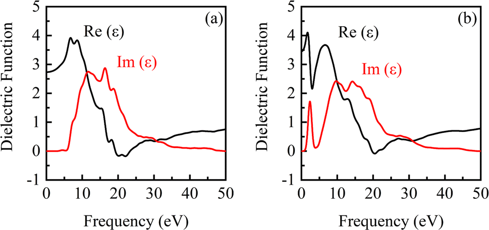 | ||
| Fig. 7 Dielectric function of β-Ga2O3 under the electric fields of 0 eV Å−1 (a) and 0.15 eV Å−1 (b). | ||
It is observed from Fig. 7 that there are a real part peak and an imaginary part of dielectric function for β-Ga2O3 without the electric field (0 eV Å−1). The dielectric response in low frequency region is faster than that in high frequency. The dielectric relaxation is significant with the increase of frequency, which is consistent with the actual situation. A deeper understanding of the dielectric function can help improve the application of β-Ga2O3 in high-frequency, low-loss power devices and photoelectric detection. After applying an electric field (0.15 eV Å−1), the real part and imaginary part peaks decrease slightly, and a new real part peak and imaginary part peak appear at about 2.0 eV and 2.5 eV, respectively. This is attributed to the excitation of the electrons from the O 2p in the valence band and its transition to Ga 4s in the conduction band, which has a lower position.
Fig. 8 shows the conductivity of β-Ga2O3 under the electric fields of 0 eV Å−1 (a) and 0.15 eV Å−1 (b). There are one real peak and one imaginary peak of conductivity for β-Ga2O3 without an electric field (0 eV Å−1). The peak in the real part is significantly lower and the valley in the imaginary part is slightly higher under the electric field of 0.15 eV Å−1 compared to that without applying an electric field. The change coincides with the results of the dielectric function, indicating that the carrier mobility of β-Ga2O3 is elevated in the presence of electric field. This is attributed to the gradual transition from a wide bandgap to a narrow band gap semiconductor under the action of electron field, where lower energy is required to excite carrier migration in the presence of light. As the wavelength gets longer, both the real and imaginary parts of the photoconductor converge to zero, indicating an increase in light utilization. It also corresponds to the fast response of the dielectric function in the low frequency region, which proves the reliability of the calculated results.
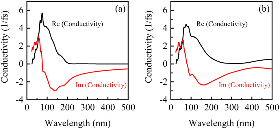 | ||
| Fig. 8 Conductivity of β-Ga2O3 under electric fields of 0 eV Å−1 (a) and 0.15 eV Å−1 (b). | ||
| N = n + ik | (2) |
The complex refraction coefficients of β-Ga2O3 with the electric fields of 0 eV Å−1 and 0.15 eV Å−1 are shown in Fig. 9. It is found that both refractive index and extinction coefficient of β-Ga2O3 have a peak without applying an electric field (0 eV Å−1). Anyway, when an electric field is applied, a new peak appears in the refractive index and extinction coefficient in the long wavelength region. The increase of real part (n) within the long wavelength range may be attributed to the slight lattice stretching of β-Ga2O3 along the electric field direction and the reduction of the band gap. New peak of the extinction coefficient induced by electric field around 500 nm, suggests that a new light absorption of β-Ga2O3 may occur in this wavelength range. To further illustrate the effect of bandgap modulation on the optical properties under the action of electric field, the optical absorption curves of β-Ga2O3 will be analyzed in the following section.
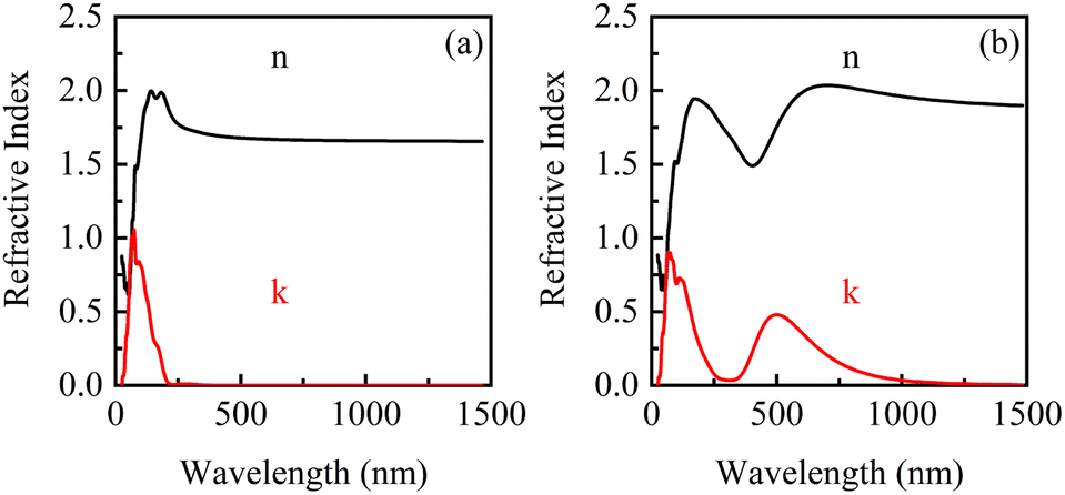 | ||
| Fig. 9 Complex refractive index of β-Ga2O3 under electric fields. (a) 0 eV Å−1, (b) 0.15 eV Å−1. | ||
Fig. 10 shows the optical absorption spectra of β-Ga2O3 with different electric field intensities. It is observed that the optical absorption curves of β-Ga2O3 are in agreement with the results of extinction coefficient. When no electric field is applied, there is only one peak in the short wavelength range. A new peak appears in the wavelength range of 400 nm to 600 nm after applying the electric field. And this absorption peak intensifies with increasing the electric field from 0.05 eV Å−1 to 0.15 eV Å−1, but weakens as the electric field intensity is over 0.15 eV Å−1, showing a maximum value with the electric field of 0.15 eV Å−1. The appearance of new peak between 400 and 600 nm may be due to three reasons.48,49 Firstly, the external electric field has a great influence on the lowest empty orbital of beta-Ga2O3, which reduces the energy gap between HOMO and LUMO orbital. Secondly, the electric field causes the change of the internal structure of beta-Ga2O3. The positive effect of the electric field on charge separation and transfer improves photocatalytic efficiency. Finally, with the help of the external potential field, the energy required for electron excitation is reduced. Weakening of optical absorption with high electric field intensity (0.20 eV Å−1) may be due to the formation of defects, which causes the change of β-Ga2O3 structure (O1–Ga2 is broken). In addition, it is also found that the absorption peak shows a blue-shift trend with the increase of electric field intensity. These results shows that the suitable electric field modulation can enhance the optical absorption of β-Ga2O3 in the visible light range which is beneficial to photocatalysis of energy conservation and environmental protection.
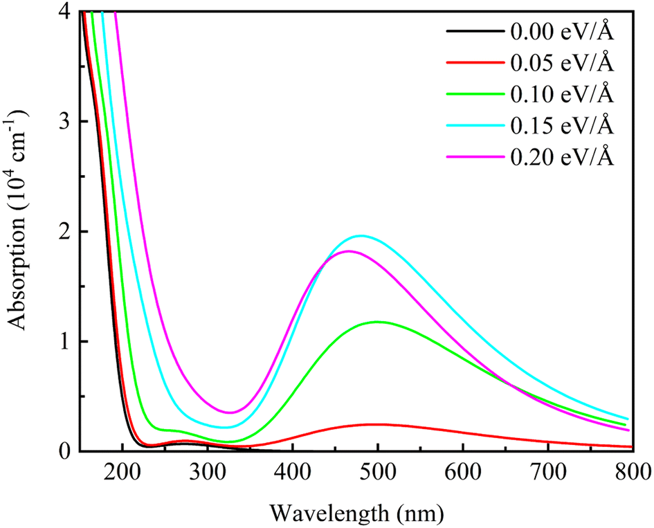 | ||
| Fig. 10 Optical absorption spectra of β-Ga2O3 under different electric fields. | ||
4. Conclusions
In conclusion, the effect of the electric field on the electronic structure and optical properties of β-Ga2O3 was investigated using the GGA+U method. The electric field in the x direction (100) was applied due to the presence of cleavage plane in this direction, and the electric field has the greatest impact on the structure of β-Ga2O3. When electric field intensity in x direction is 0.20 eV Å−1, the distance between O and Ga (O1–Ga2) parallel to the electric field direction increases to 2.52 Å. As the electric field increases from 0 eV Å−1 to 0.20 eV Å−1, the band gap of β-Ga2O3 decreases from 4.865 to 2.757 eV. The slight dispersion of the valence band and the broadening of the energy level favor the formation of a hole-conducting p-type semiconductor. At a suitable electric field intensity, the electrical conductivity of β-Ga2O3 increases and its optical absorption peak expands to the visible wavelength band. The optical absorption peak of β-Ga2O3 induced by electric field is observed in the visible light range, whose absorption properties increase by increasing electric field intensity from 0.05 to 0.15 eV Å−1. However, the absorption properties decrease when the electric field intensity is over 0.15 eV Å−1, showing a maximum value in β-Ga2O3 with the electric field of 0.15 eV Å−1, which is expected to improve the photocatalytic application of β-Ga2O3 in visible light.Data availability
The data used in this work can be made available upon reasonable request to the corresponding author.Author contributions
H. Wu: conceptualization, methodology, formal analysis, investigation, visualization, writing – original draft, review & editing, resources. C. Zhao: conceptualization, methodology, formal analysis, investigation, writing – original draft, review & editing, resources. W. Zhao: writing – review & editing, supervision. L. Li: writing – review & editing, supervision. C. Zhang: writing – review & editing, supervision.Conflicts of interest
There are no conflicts to declare.Acknowledgements
This work was financially supported by the National Natural Science Foundation of China (Grant No. 51964004).References
- J. E. N. Swallow, C. Vorwerk, P. Mazzolini, P. Vogt, O. Bierwagen, A. Karg, M. Eickhoff, J. Schörmann, M. R. Wagner, J. W. Roberts, P. R. Chalker, M. J. Smiles, P. Murgatroyd, S. A. Razek, Z. W. Lebens-Higgins, L. F. J. Piper, L. A. H. Jones, P. K. Thakur, T.-L. Lee, J. B. Varley, J. Furthmüller, C. Draxl, T. D. Veal and A. Regoutz, Chem. Mater., 2020, 32, 8460–8470 CrossRef CAS.
- Z. Galazka, Semicond. Sci. Technol., 2018, 33, 113001 CrossRef.
- Y. Tomm, J. M. Ko, A. Yoshikawa and T. Fukuda, Sol. Energy Mater. Sol. Cells, 2001, 66, 369–374 CrossRef CAS.
- A. Kuramata, K. Koshi, S. Watanabe, Y. Yamaoka, T. Masui and S. Yamakoshi, Jpn. J. Appl. Phys., 2016, 55, 1202A1202 CrossRef.
- G. Wagner, M. Baldini, D. Gogova, M. Schmidbauer, R. Schewski, M. Albrecht, Z. Galazka, D. Klimm and R. Fornari, Phys. Status Solidi A, 2014, 211, 27–33 CrossRef CAS.
- S. Kumar, C. Tessarek, G. Sarau, S. Christiansen and R. Singh, Adv. Eng. Mater., 2015, 17, 709–715 CrossRef CAS.
- M. Orita, H. Ohta, M. Hirano and H. Hosono, Appl. Phys. Lett., 2000, 77, 4166–4168 CrossRef CAS.
- U. Varshney, N. Aggarwal and G. Gupta, J. Mater. Chem. C, 2022, 10, 1573–1593 RSC.
- M. Higashiwaki, K. Sasaki, A. Kuramata, T. Masui and S. Yamakoshi, Phys. Status Solidi A, 2014, 211, 21–26 CrossRef CAS.
- Z. Hu, H. Zhou, Q. Feng, J. Zhang, C. Zhang, K. Dang, Y. Cai, Z. Feng, Y. Gao, X. Kang and Y. Hao, IEEE Electron Device Lett., 2018, 39, 1564–1567 CAS.
- M. Navarrete, S. Cipagauta-Díaz and R. Gómez, J. Chem. Technol. Biotechnol., 2019, 94, 3457–3465 CrossRef CAS.
- B. Zhao, F. Wang, H. Chen, L. Zheng, L. Su, D. Zhao and X. Fang, Adv. Funct. Mater., 2017, 27, 1700264 CrossRef.
- W. Yang, X. Zhang, H. Tan, D. Yang, Y. Feng, X. Rui and Y. Yu, J. Energy Chem., 2021, 55, 557–571 CrossRef CAS.
- X. Tang, X. Huang, Y. Huang, Y. Gou, J. Pastore, Y. Yang, Y. Xiong, J. Qian, J. D. Brock, J. Lu, L. Xiao, H. D. Abruña and L. Zhuang, ACS Appl. Mater. Interfaces, 2018, 10, 5519–5526 CrossRef CAS PubMed.
- Y. Huang, X. Tang, J. Wang, H. Ma, Y. Wang, W. Liu, G. Wang, L. Xiao, J. Lu and L. Zhuang, Langmuir, 2019, 35, 13607–13613 CrossRef CAS PubMed.
- J. Guo, F. Gao, D. Li, X. Luo, Y. Sun, X. Wang, Z. Ran, Q. Wu and S. Li, ACS Sustainable Chem. Eng., 2020, 8, 13692–13700 CrossRef CAS.
- G. Meligrana, W. Lueangchaichaweng, F. Colò, M. Destro, S. Fiorilli, P. P. Pescarmona and C. Gerbaldi, Electrochim. Acta, 2017, 235, 143–149 CrossRef CAS.
- M. Yang, C. Sun, T. Wang, F. Chen, M. Sun, L. Zhang, Y. Shao, Y. Wu and X. Hao, ACS Appl. Energy Mater., 2018, 1, 4708–4715 CrossRef CAS.
- K. Wang, W. Ye, W. Yin, W. Chai, B. Tang and Y. Rui, Dalton Trans., 2019, 48, 12386–12390 RSC.
- C. Zhang, F. Liao, X. Liang, H. Gong, Q. Liu, L. Li, X. Qin, X. Huang and C. Huang, Phys. B, 2019, 562, 124–130 CrossRef CAS.
- J. Zhang, B. Li, C. Xia, G. Pei, Q. Deng, Z. Yang, W. Xu, H. Shi, F. Wu, Y. Wu and J. Xu, J. Phys. Chem. Solids, 2006, 67, 2448–2451 CrossRef CAS.
- C. J. Zeman, S. M. Kielar, L. O. Jones, M. A. Mosquera and G. C. Schatz, J. Alloys Compd., 2021, 877, 160227 CrossRef CAS.
- L. Li, F. Liao and X. Hu, Superlattices Microstruct., 2020, 141, 106502 CrossRef CAS.
- W. Liang, L. Hong, H. Yang, F. Fan, Y. Liu, H. Li, J. Li, J. Y. Huang, L.-Q. Chen, T. Zhu and S. Zhang, Nano Lett., 2013, 13, 5212–5217 CrossRef CAS PubMed.
- R. D. Deshpande, J. Li, Y.-T. Cheng and M. W. Verbrugge, J. Electrochem. Soc., 2011, 158, A845 CrossRef CAS.
- J. Kang, F. Wu and J. Li, J. Phys.: Condens. Matter, 2012, 24, 165301 CrossRef PubMed.
- L. Feng, X. Zhang and G. Xiang, Comput. Mater. Sci., 2021, 198, 110697 CrossRef CAS.
- Y. Zhang, J. Yan, G. Zhao and W. Xie, Phys. B, 2010, 405, 3899–3903 CrossRef CAS.
- L. Zhang, J. Yan, Y. Zhang, T. Li and X. Ding, Phys. B, 2012, 407, 1227–1231 CrossRef CAS.
- X. Cai, F. P. Sabino, A. Janotti and S.-H. Wei, Phys. Rev. B, 2021, 103, 115205 CrossRef CAS.
- N. Martsinovich, D. R. Jones and A. Troisi, J. Phys. Chem. C, 2010, 114, 22659–22670 CrossRef CAS.
- S. Piskunov, E. Heifets, R. I. Eglitis and G. Borstel, Comput. Mater. Sci., 2004, 29, 165–178 CrossRef CAS.
- Y. Wang, H. Yin, R. Cao, F. Zahid, Y. Zhu, L. Liu, J. Wang and H. Guo, Phys. Rev. B: Condens. Matter Mater. Phys., 2013, 87, 235203 CrossRef.
- S. Geller, J. Chem. Phys., 2004, 33, 676–684 CrossRef.
- L. Dong, R. Jia, B. Xin, B. Peng and Y. Zhang, Sci. Rep., 2017, 7, 40160 CrossRef CAS PubMed.
- J. Liu, S. Gao, W. Li, J. Dai, Z. Suo and Z. Suo, Cryst. Res. Technol., 2022, 57, 2100126 CrossRef CAS.
- T. Zheng, Q. Wang, J.-n. Dang, W. He, L.-y. Wang and S.-w. Zheng, Comput. Mater. Sci., 2020, 174, 109505 CrossRef CAS.
- M. C. Payne, M. P. Teter, D. C. Allan, T. A. Arias and J. D. Joannopoulos, Rev. Mod. Phys., 1992, 64, 1045 CrossRef CAS.
- W. S. Hwang, A. Verma, H. Peelaers, V. Protasenko, S. Rouvimov, H. Xing, A. Seabaugh, W. Haensch, C. V. de Walle, Z. Galazka, M. Albrecht, R. Fornari and D. Jena, Appl. Phys. Lett., 2014, 104, 203111 CrossRef.
- J. B. Varley, A. Janotti, C. Franchini and C. G. Van de Walle, Phys. Rev. B: Condens. Matter Mater. Phys., 2012, 85, 081109 CrossRef.
- J. L. Lyons, Semicond. Sci. Technol., 2018, 33, 05LT02 CrossRef.
- K. H. Khoo, M. S. C. Mazzoni and S. G. Louie, Phys. Rev. B: Condens. Matter Mater. Phys., 2004, 69, 201401 CrossRef.
- M. Raeiszadeh and B. Adeli, ACS Photonics, 2020, 7, 2941–2951 CrossRef CAS PubMed.
- B. H. Lado and A. E. Yousef, Microbes Infect., 2002, 4, 433–440 CrossRef PubMed.
- I. Hamzavi and H. Lui, Dermatol. Clin., 2005, 23, 199–207 CrossRef PubMed.
- L. Guo, Y. Guo, J. Wang and T. Wei, J. Semicond., 2021, 42, 081801 CrossRef CAS.
- R. P. Gallagher and T. K. Lee, Prog. Biophys. Mol. Biol., 2006, 92, 119–131 CrossRef CAS PubMed.
- G. L. Xu, W. J. Lv, Y. F. Liu, Z. L. Zhu, X. Z. Zhang and J. F. Sun, Acta Phys. Sin., 2009, 58(05), 3058–3063 CrossRef CAS.
- Z. Lou, P. Wang, B. Huang, Y. Dai, X. Qin, X. Zhang, Z. Wang and Y. Liu, ChemPhotoChem, 2017, 1, 136 CrossRef CAS.
| This journal is © The Royal Society of Chemistry 2023 |