
 Open Access Article
 This Open Access Article is licensed under a Creative Commons Attribution-Non Commercial 3.0 Unported Licence
Nanocomposites of chalcogenide phase-change materials: from C-doping of thin films to advanced multilayers†
Rebecca
Chahine
a,
Martina
Tomelleri
a,
Jessy
Paterson
a,
Mathieu
Bernard
a,
Nicolas
Bernier
a,
François
Pierre
a,
Denis
Rouchon
a,
Audrey
Jannaud
a,
Cristian
Mocuta
b,
Valentina M.
Giordano
 c,
Françoise
Hippert
d and
Pierre
Noé
*a
c,
Françoise
Hippert
d and
Pierre
Noé
*a
aUniversité Grenoble Alpes, CEA, LETI, Grenoble F-38000, France. E-mail: pierre.noe@cea.fr
bSynchrotron SOLEIL, F-91192 Gif-sur-Yvette, France
cILM, UMR 5306 Univ. Lyon 1-CNRS, Villeurbanne Cedex F-69622, France
dUniversité Grenoble Alpes, CNRS, Grenoble INP, LMGP, Grenoble F-38000, France
First published on 10th November 2022
Abstract
Engineering of chalcogenide phase-change materials at the nanoscale is required to improve the performances of ultimate size memory devices and reduce their power consumption. Amorphous C-doped GeTe thin films and innovative multilayers consisting of periodic stacks of a few nm thick GeTe, or Ge2Sb2Te5, and C layers with a thickness between 0.5 and 2 nm are deposited by magnetron sputtering at room temperature. The phase-change material is then crystallized by heat treatment. In C-doped GeTe films, the phase separation of C and GeTe during the GeTe crystallization leads to the spontaneous formation of a nanocomposite, consisting of amorphous C located at the grain boundaries of GeTe crystallites, but the resulting nanostructure is highly disordered. In contrast, the deposition of multilayers allows control of the nanostructure and the interfaces between the phase-change material and the C phase. Transmission electron microscopy and X-ray diffraction at room temperature and as a function of temperature during annealing show that the multilayer structure is maintained after crystallization of the phase-change material, even when the thickness of the C layer is as low as 0.5 nm. GeTe and Ge2Sb2Te5 crystallites are anisotropic, their size in the direction perpendicular to the layers being determined by the design of the multilayer. The crystallisation temperature of the GeTe and Ge2Sb2Te5 layers depends on the structure of the stack, revealing scaling and stress effects. The results presented show that GeTe/C and Ge2Sb2Te5/C MLs are promising for applications in memory devices and also in photonic and thermoelectric devices.
1. Introduction
Chalcogenide phase-change materials (PCMs), such as Ge–Sb–Te alloys lying on the pseudo-binary GeTe–Sb2Te3 tie line exhibit fast and reversible phase transformations between crystalline and amorphous states with very different transport and optical properties.1 Their outstanding properties led to their integration in resistive phase-change memories.2 These are now considered a mature technology as they are already entering the memory market through an innovative 3D cross-point architecture.3,4 PCM memories have good endurance, very high scalability, multi-level storage capability and good data retention.2 They are also very promising in the fields of in-memory computing and artificial intelligence. Innovative PCM-based devices can mimic the synaptic functions of the human brain for neuromorphic computing purposes, far beyond the classical von Neumann computing architecture of most current computers.5,6 In a memory device, current pulses are applied to change the structural state, and hence the resistance, of a small volume of the PCM, and thus encode the information. A high current pulse (RESET) is applied to amorphize the PCM (leading to a high resistance state). A lower current pulse (SET) allows recrystallization of the PCM (leading to a low resistance state). Prototypical PCM alloys are Ge2Sb2Te5 (GST), one of the ternary Ge–Sb–Te alloys of the GeTe–Sb2Te3 tie line, and GeTe, at one end of the tie line. The programming performances of GST and GeTe devices are similar.7 GeTe has a higher retention to GST with a crystallization temperature of ∼230 °C, with respect to ∼170 °C for GST, for non-oxidized films.8 In addition to memory applications, GeTe is also very promising for RF switches,9 for thermoelectrics,10,11 and offers numerous opportunities for optical applications12 and photonics13 as well as for the emerging field of spintronics.14PCM memories are currently the most promising technology for storage class memory (SCM) applications, but they still have to overcome several technological issues. In order to reduce power consumption, it is necessary to reduce the programming currents, in particular during the RESET operation. To this end, the most used strategy has been to optimize the architecture of the memory device in order to improve the thermal confinement and reduce the size of the active PCM volume inside the memory cell, thus limiting the energy wasted when programming the cell by Joule heating.1,2,5 An alternative approach is to optimize the phase-change material. In a memory device, the small volume that is amorphized during the RESET pulse is surrounded by polycrystalline PCM. Reducing the thermal conductivity of the polycrystalline state of PCM therefore allows for better thermal confinement during the RESET pulse, which reduces the thermal budget needed to reset the memory cell. To this end, engineering of chalcogenide phase-change materials at the nanoscale is a promising approach, as in nanocomposites the thermal conductivity can be greatly reduced due to phonon scattering at the interfaces, especially when the contrast of properties between the components is large.15–19
A reduction in the RESET current in memory devices has been achieved by adding C or N, at relatively high concentration (a few percent), in GST or GeTe.7,20–23 The nanostructure of crystallized C-doped GST has been studied in detail.23–25 In the amorphous state, C atoms are incorporated into the GST phase, preferentially forming strong Ge–C covalent bonds, as well as C–C bonds in C chains.23,24 In contrast, most of the C atoms are expelled from the GST phase during its crystallization. Nanometre-size carbon clusters have been detected using transmission electron microscopy23,25 and atom probe tomography,24 while a small fraction of the C atoms could remain in the crystalline GST phase.23,25 The necessity to expel C atoms from the GST phase during its crystallization explains the increase in the crystallization temperature as the carbon content increases. The size of GST crystallites decreases with increasing carbon content.20,23 The thermal conductivity of crystallized C-doped GST films is lower than that of undoped GST,22,23 which must be related to their nanostructure consisting of C clusters and GST crystallites. Reduced thermal conductivity allows an improved thermal confinement of the heat during the RESET process in memory devices incorporating C-doped GST and thus contributes to the observed reduction in RESET current with respect to devices incorporating undoped GST. However, the spontaneous separation of the C and GST phases during GST crystallization leads to a highly disordered nanostructure with C nanoclusters of different sizes and a broad size distribution of PCM crystallites, resulting in disordered interfaces and an uncontrolled density of chemical heterogeneities. Carbon segregation leads to variability in PCM devices and will not allow further reduction in device size, hence the need for other types of C and PCM nanostructures, combining controlled interfaces and a low thermal conductivity.
For this purpose, a multilayer (ML) structure consisting of a periodic stacking of PCM layers alternating with spacer layers seems interesting. Studies of PCM multilayers have been reported in the literature with Sb2Te3, Sb, GaSb or SnSb4 as the spacer material between the PCM layers.26–29 In these cases, the spacer layer crystallizes during the heat treatment applied to crystallize the PCM. Furthermore, in the case of Sb or Sb2Te3 spacer layers, intermixing with PCM layers is unavoidable during heating.30,31 Recently, improved programming performances were achieved in devices incorporating a TiTe2/Sb2Te3 multilayer where the TiTe2 layers act as an efficient thermal barrier during the RESET process.32
In the present work, we investigate the structure of GeTe/C and GST/C multilayers (MLs) in which a few nm thick GeTe or GST layers are separated by ultrathin amorphous C layers (thickness of 0.5, 1 or 2 nm). Compared to previous studies of MLs, the choice of amorphous C as a spacer material should have several advantages. First, considering the nanostructure observed in crystallized C-doped GST films, intermixing between the amorphous C layers and crystallized PCM layers should be negligible. Second, due to the significant difference in the elastic properties of amorphous C and crystallized PCM, the high density of PCM/C interfaces at a length scale close to that of the phonon mean free path should increase phonon scattering, thereby reducing the thermal conductivity of the ML structure.
The GeTe/C and GST/C MLs were deposited by sputtering at room temperature. The initially amorphous PCM layers were then crystallized by heat treatment. The nanostructure of the MLs was investigated in detail by X-ray diffraction (XRD) and transmission electron microscopy (TEM) and compared to that of C-doped GeTe films. The results show that a high-quality GeTe/C or GST/C ML structure is maintained after crystallization of the PCM layers, even when the amorphous C layers are as thin as 0.5 nm. Contrary to the recent results reported by Zheng et al.,33 no C clusters are observed in crystallized GST/C multilayers. In the studied MLs, the size of the GeTe or GST crystallites in the direction perpendicular to the layers is determined solely by the multilayer design. Their size in the plane of the layers is larger, with differences between GeTe/C and GST/C MLs that can be attributed to the different crystallization mechanisms of GeTe and GST.8,34–36 For a given C layer thickness, the crystallization temperature of the GeTe and GST layers increases slightly as the thickness of the PCM layer decreases from 9 to 2 nm, revealing scaling and stress effects.
These results demonstrate that the choice of C as the spacer material in a ML structure allows full control of the interfaces between crystalline PCM and amorphous C phases. Moreover, the fact that a ML nanostructure is retained after annealing at 400–450 °C allows integration of these MLs in memory devices, as we have recently shown.37
2. Experimental
2.1. Film deposition
GeTe/C and GST/C ML films were deposited at room temperature under an Ar atmosphere by magnetron sputtering on Si(100) wafers of 200 mm in diameter in an ultra-high vacuum industrial tool (EVATEC ClusterLine200TM) by alternating sputtering of a C target and of a GeTe (or a GST) target. Films were deposited on Si substrates previously de-oxidized by Ar sputtering and on Si substrates covered by a 500 nm thick SiO2 layer obtained by thermal oxidation. In a given ML, the thickness of the PCM and C layers is kept constant. Different GeTe/C and GST/C MLs were deposited with the thickness of the PCM layer varying between 19 and 2 nm and a thickness of the C layer equal to either 0.5, 1 or 2 nm. The thickness of the PCM and C layers was varied by changing the deposition times, while keeping the other deposition parameters constant. In order to determine the deposition times of each material, a series of GeTe, GST and C thin films of varying thicknesses were deposited using the same sputtering conditions as for MLs. The thickness of these calibration films was measured by X-ray reflectivity. In a given ML, the number of PCM/C bilayers was chosen so that the total thickness of the ML film was close to 100 nm. The MLs are denoted, for example, [GeTe 4 nm/C 0.5 nm]22 where the subscript is the number of GeTe/C bilayers. All MLs were protected against oxidation by depositing in situ, immediately after fabrication, a 10 nm thick SiN capping layer. Exposure to air is known to lead to oxidation of GeTe and GST and affect the crystallization mechanism.8,36As-deposited MLs with a PCM layer thickness equal to 4 nm were characterized by time of flight secondary ion mass spectrometry (ToF-SIMS) (Fig. S1, ESI†). The SIMS depth profiles of Ge, Sb, Te and C ions show clear periodic oscillations as a function of the sputtering time. For all MLs, the number of periods coincides with that expected. The oscillations of the Ge, Sb and Te depth profiles are in phase and are clearly shifted with respect to the oscillations of the C profile. These SIMS results demonstrate that the deposition method allows fabrication of high quality GeTe/C and GST/C MLs.
C-doped GeTe and GST films (100 or 150 nm thick) were deposited by co-sputtering of a C target and a GeTe (or GST) target. The C content in the doped films was varied between 5.8 at% and 25 at% by changing the power applied to the C target. Reference GeTe films of 50 and 100 nm thickness and a GST film of 100 nm thickness were also deposited using the same sputtering conditions.
The Ge, Sb and Te contents in the as-deposited C-doped and ML films were determined by means of ion-beam analysis techniques using Rutherford backscattering (RBS) combined with particle induced X-ray emission (PIXE). The C content was determined by nuclear reaction analysis (NRA). Measurements were performed at ARCANE (CENBG, Gradignan, France). The data are reported in Table S2 (ESI†).
All films are amorphous after deposition. For characterization purposes, pieces of the films were then submitted to thermal treatments under a high N2 gas flow in order to crystallize the GeTe or GST phase. The annealing temperatures are specified below for each case.
2.2. FTIR and Raman spectroscopies and sheet resistance measurement
The absorbance of amorphous and crystallized C-doped GeTe films deposited on a Si substrate was measured at room temperature in transmission mode by using BIO-RAD QS500 and Brucker VERTEX 80V Fourier transform infrared (FTIR) spectrometers, which allow measurements from 50 to 400 cm−1 and from 400 to 2000 cm−1, respectively. All absorbance spectra were acquired under the same experimental conditions (average over 32 scans and spectral resolution of 2 cm−1). An absorbance spectrum measured on a Si substrate covered with a 10 nm SiN capping layer was used to subtract the background from all FTIR spectra measured on C-doped GeTe films.Raman scattering spectra were acquired at room temperature by using a RENISHAW micro-Raman spectrometer operating in the range from 900 to 2000 cm−1 and using a laser probe at a wavelength of 532 nm. The acquisition conditions (laser power, magnification and exposure time) were adjusted in order to optimize the signal-to-noise ratio. In order to avoid any change or damage to the material that could result from the impact of the high fluence laser on the film surface during the acquisition of the Raman signal, the damage power threshold was first determined by progressively increasing the laser power until a change in the Raman spectrum of the probed sample was observed. Then, the Raman spectra were acquired by using a power well under the damage power threshold.
The sheet resistance (Rs) of C-doped and ML films deposited on an insulating SiO2 buffer was measured as a function of temperature by the four-point probe technique. The initially amorphous films were heated up to 500 °C at a rate of 10 °C min−1 and then cooled down to room temperature at the same rate. During the measurement, the samples were exposed to a high flow of N2 gas to avoid oxidation. In a four-probe measurement, the applied current flows parallel to the film surface. In the case of a homogeneous film, the resistivity ρ in the plane of the film is equal to Rs·t, where t is the thickness of the film. This relationship cannot be used to obtain the resistivity of the GeTe layers in a ML and only the Rs values are presented below.
2.3. Scanning transmission electron microscopy imaging
Bright field (BF) and high-angle annular dark-field (HAADF) scanning transmission electron microscopy (STEM) images were acquired at room temperature on a probe and image Cs-corrected FEI Titan Ultimate microscope operating at 200 kV. Cross-sectional STEM foils were obtained in two steps. The film was first mechanically thinned with a tripod polisher down to a thickness of about 10 μm. The obtained foil was then Ar-ion milled using a Gatan precision ion polishing system (PIPS) at an accelerating voltage of 3 kV and milling angles of 5°. The final thickness of the STEM foil was estimated to be around 20–30 nm. STEM electron energy loss spectroscopy (EELS) maps were acquired in dual-EELS mode from 200 to 2100 eV with a dispersion of 0.5 eV per channel. Standard processing of the spectra was performed by using Gatan microscopy suite (GMS) software to obtain the elemental maps.2.4. X-ray diffraction experiments
Out-of-plane X-ray diffraction (XRD) patterns were measured at room temperature on crystallized GeTe/C and GST/C ML films and on C-doped and reference GeTe and GST films by using a PANalytical Empyrean diffractometer (CuKα radiation) in the ω–2θ geometry. The ω value differed from θ by a small constant offset of 2°. In-plane XRD patterns were measured at room temperature by using a Rigaku SMART-lab diffractometer (CuKα radiation) with an incident angle set to 0.5°. For both diffraction geometries, reference Si powder was measured to determine the contribution of the instrument to the diffraction peak width. Besides, temperature-resolved X-ray diffraction data were collected on two GeTe/C MLs and on a reference GeTe film at Synchrotron SOLEIL on the DiffAbs beamline, using a 6-circle diffractometer in kappa geometry. The X-ray beam was monochromatized (ΔE/E ∼ 10−4) using a Si(111) double crystal monochromator and was focused in the vertical and horizontal direction to a size of 184 × 266 μm2 (full width at half maximum). The typical divergence of the resulting X-ray beam was ∼0.01° × 0.1° (full width at half-maximum, vertical × horizontal). The wavelength was set to 0.6908 Å, and calibrated by measuring the diffraction pattern of a standard reference material (CeO2 powder) from the National Institute of Standards and Technology (NIST). Crystallization of the initially amorphous films was monitored by measuring diffraction patterns during heating at a rate of 2 °C min−1. The heating stage (Anton Paar furnace DHS 900) was equipped with a homemade dome with Kapton windows for the incident and scattered beams, in order to reduce the dome scattering. The samples were heated under a continuous N2 flow. The angle between the incident beam and the film's surface was fixed to 3°. A two-dimensional (2D) X-ray hybrid pixel array detector (XPAD) was used.38 The scattered intensities as a function of the scattering angle 2θ were obtained by azimuthal integration of the 2D image.39 The integration range is ±10° for 2θ = 13°. A diffraction pattern in the 2θ range [9.5–25°] with a 2θ-step equal to 0.0194° was generated by acquiring images (acquisition time of 30 s per image) for two positions of the 2D detector. After completing the acquisition of the two images, an adjustment of the film vertical position was performed to compensate the thermal dilatation of the sample holder in the furnace. XRD patterns were also acquired during cooling at a faster rate of 20 °C min−1.3. Results
3.1. Nanostructure of C-doped GeTe films
In amorphous C-doped GeTe films, the C atoms are bonded to Ge and Te atoms and increase the rigidity of the amorphous state.40,41 In order to investigate the structural changes induced by crystallization, we have studied the vibration modes of a C-doped GeTe film (C content 20 ± 1 at%) by FTIR spectroscopy at room temperature. Pieces of the as-deposited 150 nm thick film were heated to different temperatures (Tann) at a rate of 10 °C min−1 and cooled down to room temperature in a few minutes. The FTIR absorbance spectra are shown in Fig. 1. Intense vibration modes are detected in the 400–2000 cm−1 range as long as the film is amorphous (Tann ≤ 350 °C). These modes are the signature of C atoms in the GeTe phase, as illustrated in Fig. 1. No vibration modes are detected in this range in an undoped GeTe film (see Fig. S3, ESI†).42 A comparison with ab initio simulations shows that C–Ge and C–Te bonds in tetrahedral units centred on C atoms lead to vibration modes between 400 and 800 cm−1 and C–C bonds in C chains bonded to at least one Ge or Te atom lead to modes between 1400 and 1900 cm−1.41 Strikingly, none of these modes are detected, within the experimental accuracy, for Tann = 450 °C after full crystallization of the C-doped GeTe film. For Tann = 400 °C, a weak absorbance may be present around 600 cm−1, which could be due to incomplete crystallization of GeTe. A clear signature of the presence of a crystallized GeTe phase in the films annealed at 400 and 450 °C is provided by the intense vibration modes detected below 200 cm−1. These modes are characteristic of the octahedral units present in the rhombohedral α-GeTe phase.42,43 Note that an intense absorption due to the presence of free carriers appears after GeTe crystallization. Despite a large band gap, the rhombohedral α-GeTe phase exhibits semi-metallic conduction, due to a large number of holes resulting from the existence of Ge vacancies.44 The baseline resulting from the free carrier absorbance was subtracted from the absorbance spectra of the crystalline films to obtain similar absorbance scales for the crystalline and amorphous films in Fig. 1. This explains the increase in noise in the absorbance curves when Tann reaches 400 °C.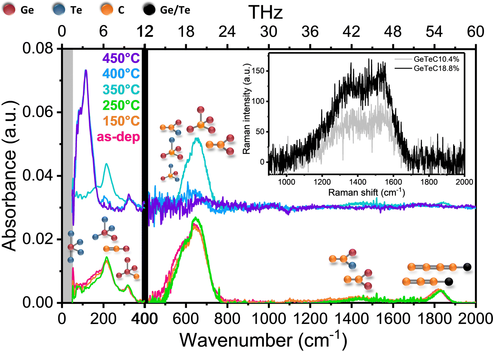 | ||
| Fig. 1 Room temperature FTIR absorbance spectra of 150 nm thick C-doped GeTe films (C content 20 ± 1 at%). The as-deposited film and the films annealed at 150 °C, 250 °C and 350 °C are amorphous. The vibration modes detected above 400 cm−1 are the signature of C atoms in the amorphous GeTe phase. These modes are absent in the fully crystallized film annealed at 450 °C. The FTIR spectra of films annealed at 350 °C, 400 °C and 450 °C are vertically shifted for clarity. Inset: Room temperature Raman spectra of 100 nm thick C-doped GeTe films (C content 10.4 ± 0.6 and 18.8 ± 1.1 at%), crystallized by annealing at 500 °C, showing the presence of an amorphous carbon phase. | ||
The FTIR results clearly show that the C atoms are expelled from the GeTe phase during its crystallization. In addition, the existence of an amorphous carbon phase in crystallized C-doped GeTe films could be proven by Raman spectroscopy. 100 nm thick amorphous films (C content of 10.4 ± 0.6 and 18.8 ± 1 at%) were fully crystallized by annealing at 500 °C. A broad Raman signal is observed in the 1000–1700 cm−1 range (inset of Fig. 1). It exhibits the characteristics of amorphous carbon obtained by sputtering with the coexistence of sp2 and sp3 hybridization, as shown by the presence of broad D and G bands (expected around 1415 and 1580 cm−1), as well as a less intense Raman signal near 1180 and 1332 cm−1.45
These results show that phase separation between the amorphous carbon phase and the crystalline GeTe phase occurs during the crystallization of GeTe in C-doped GeTe films. To obtain insight into this phase separation at the nanoscale, we acquired STEM images and EELS elemental maps on a 100 nm thick GeTe film doped with 8.6 ± 0.6 at% C (Fig. 2). This film was fully crystallized by annealing at 450 °C. Special care was taken in the preparation of the STEM foil to reduce its thickness to a few nm in order to study the grain boundaries. A STEM image in bright field mode of a selected part of the foil (Fig. 2(a)) allows detection of crystallized GeTe grains with a size in the order of 10–20 nm. An image of the entire foil acquired in the HAADF-STEM mode is shown in Fig. 2(b). Thin dark lines are clearly visible. They form a disordered interconnected network. Their typical thickness is ≈1 nm. A few dark spots (size ≈ 5 nm) are also detected. In the HAADF mode, the contrast is mainly due to the Z differences between elements, with an intensity I ∼ Z1.7, and thus the brighter areas correspond to the heavier atoms.46 These observations suggest that the carbon phase tends to surround the GeTe crystallites, with, in a few locations, an accumulation of C atoms in nm-size carbon clusters. EELS maps acquired in a representative frame (20 × 20 nm2) fully confirm the interpretation of the HAADF image. The superposition of the Te and C maps shown in Fig. 2(c) highlights the phase separation between the C and GeTe phases.
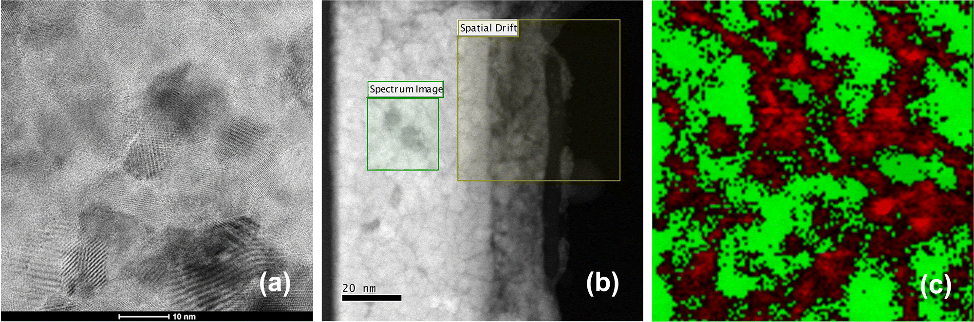 | ||
| Fig. 2 BF-STEM image (a) and HAADF-STEM image (b) of a 100 nm thick GeTe film doped with 8.6 ± 0.6 at% C fully crystallized by annealing at 450 °C. (c) Superimposed EELS maps of C (in red) and Te (in green) acquired within the green frame (20 × 20 nm2) shown in (b). The yellow frame in (b) has been used to compensate the spatial drift during the acquisition of the EELS maps. | ||
The detection of low intensity modes around 300 cm−1 in the FTIR spectra of the amorphous and crystallized C-doped GeTe film in Fig. 1 deserves additional comment. Modes in this frequency range are observed in amorphous and crystalline Ge by Raman spectroscopy.47,48 They are due to Ge–Ge vibrations in tetrahedral Ge4 units. In amorphous C-doped GeTe films, the Ge/Te ratio being larger than 1 (Table S2, ESI†), the presence of Ge–Ge3C tetrahedral units is expected. Thus, the modes detected by FTIR around 300 cm−1 can be attributed to Ge–Ge vibrational modes in Ge–Ge3C units, these modes being optically active in IR absorption spectroscopy due to the presence of the C atom. In crystallized C-doped films, Ge precipitates must coexist with GeTe crystallites since the crystalline GeTe phase is slightly deficient in Ge,49 Thus, Ge–Ge3C tetrahedral units could be present either in the Ge phase, if it contains some C atoms, or at the interfaces between the carbon phase and the Ge precipitates, which would explain the persistence of vibration modes around 300 cm−1 in crystallized C-doped films.
In summary, in C-doped GeTe films, the phase separation of C and GeTe when the GeTe phase crystallizes leads to the spontaneous formation of a nanocomposite in which GeTe crystallites coexist with an amorphous carbon phase. Within the experimental accuracy of the FTIR spectra, that there are no C atoms in the crystalline GeTe phase. The nanostructure resulting from this phase separation is highly disordered. In contrast, as shown below, the deposition of GeTe/C MLs allows the interfaces between the GeTe and carbon phases to be defined and controlled.
3.2. Nanostructure of GeTe/C multilayers
The crystallization of GeTe/C ML films was monitored using temperature-resolved sheet resistance (Rs) measurements. Rs curves are shown in Fig. 3(a) for three GeTe/C MLs with the same thickness of the GeTe layer (4 nm) and different C layer thickness (0.5, 1 or 2 nm) and for a reference 100 nm thick GeTe film. Curves for other MLs are shown in Fig. S4 (ESI†). In all cases, a drop in Rs of several orders of magnitude is observed during heating. This is due to the crystallization of GeTe, as confirmed below by STEM and XRD. The crystallization temperature Tx is usually defined in the literature as the temperature of the minimum of the derivative of the Rs curve. This definition is relevant for the GeTe film (Tx = 230 °C) and for the [GeTe 4 nm/C 0.5 nm]22 ML (Tx = 244 °C) that show an abrupt drop in Rs. For the [GeTe 4 nm/C 1 nm]20 and [GeTe 4 nm/C 2 nm]17 MLs, the Rs change is less abrupt and the obtained Tx values (258 °C and 290 °C, respectively) must be taken as indicative. A moderate increase in Tx is observed as the thickness of the C layer increases from 0.5 to 2 nm.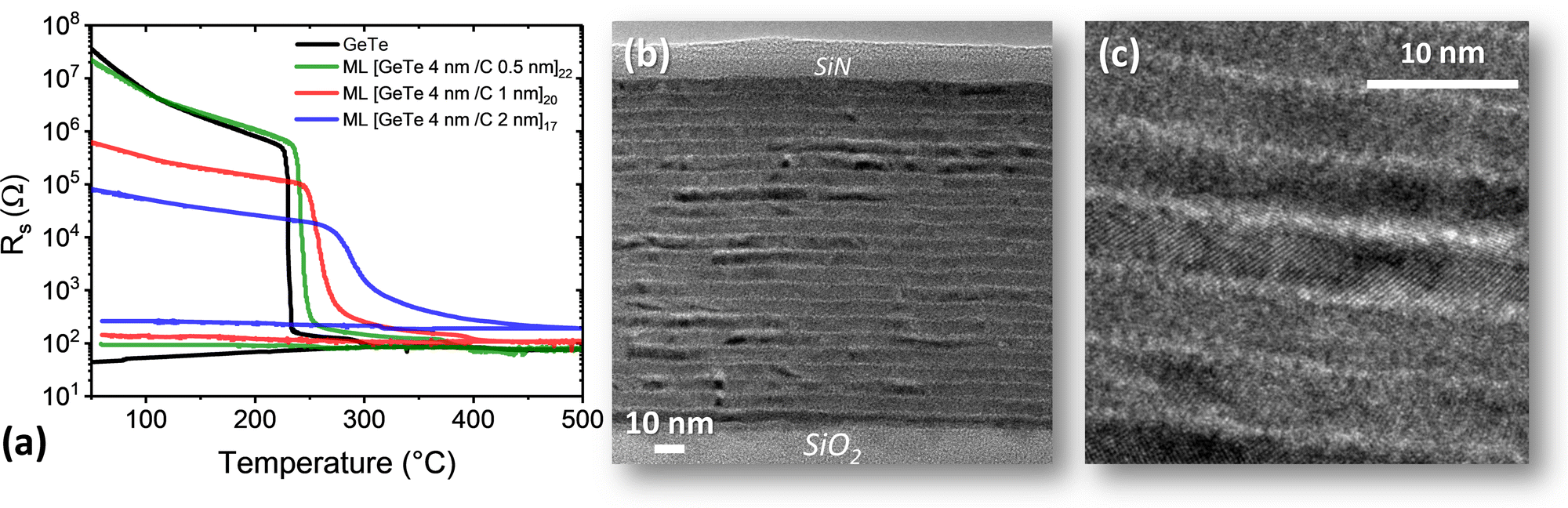 | ||
| Fig. 3 (a) Sheet resistance as a function of temperature when heating up to 500 °C and cooling (ramp rate of 10 °C min−1) for a 100 nm thick reference GeTe film and for GeTe/C multilayer (ML) films. The as-deposited films are amorphous. In all films, a drop in resistance of several orders of magnitude is observed upon heating during the crystallization of GeTe. (b and c) BF-STEM images of a [GeTe 4 nm/C 0.5 nm]22 ML film deposited on SiO2 and capped with a 10 nm thick SiN layer and then annealed at 300 °C for 15 minutes. Bright C layers alternate with darker GeTe layers in which crystallized grains are clearly visible. | ||
The Rs values measured, at a given temperature, in the three amorphous MLs vary by several orders of magnitude. These changes must be related to changes in the total thickness of the C layers. The room temperature resistivity of a 10 nm thick C film, deposited by sputtering in the same deposition conditions as the C layers in the MLs, is ≈3 Ω cm. Although the resistivity of the C layers certainly depends on their thickness, it can be concluded from this measured value that the resistivity of the C layers in MLs is much lower than that of the amorphous GeTe layers. Thus, the current applied to measure Rs flows mainly in the C layers. In contrast, in crystallized MLs, the resistivity of the C layers is much larger than that of the crystallized GeTe layers and the current flows mainly in the GeTe layers.
The ratio between the numbers of Ge and Te atoms is 1.18 ± 0.1 in all films (Table S2, ESI†), whereas, as mentioned above, the crystalline GeTe phase is slightly deficient in Ge.49 In GeTe films, crystallization of the GeTe phase leads to the formation of amorphous Ge precipitates that crystallize at a higher temperature than the GeTe phase, as clearly shown by temperature-resolved XRD (ref. 50 and Fig. 4(a)). The Ge crystallization leads to the small drop in Rs observed in a 20 °C range around 297 °C upon heating in the reference GeTe film (Fig. 3(a)). Similar small drops in Rs are observed around 381 °C in the [GeTe 4 nm/C 0.5 nm]22 ML and 395 °C in the [GeTe 4 nm/C 1 nm]20 ML (see the enlarged view in Fig. S5, ESI†). They can be ascribed to the crystallization of excess Ge in the GeTe layers. Consistently, the presence of a crystalline Ge phase is detected by room temperature XRD experiments in these two ML films after annealing at 425 °C (Fig. S5, ESI†). This is not the case in a [GeTe 4 nm/C 2 nm]17 ML film annealed at 425 °C. The excess of Ge being the same in all MLs (Table S2, ESI†), the crystallization of Ge in the [GeTe 4 nm/C 2 nm]17 ML is thus expected to occur above 425 °C. Although no clear drop in Rs is detected in the [GeTe 4 nm/C 2 nm]17 between 425 °C and 500 °C, a small change of curvature occurring around 475 °C could indicate the Ge crystallization.
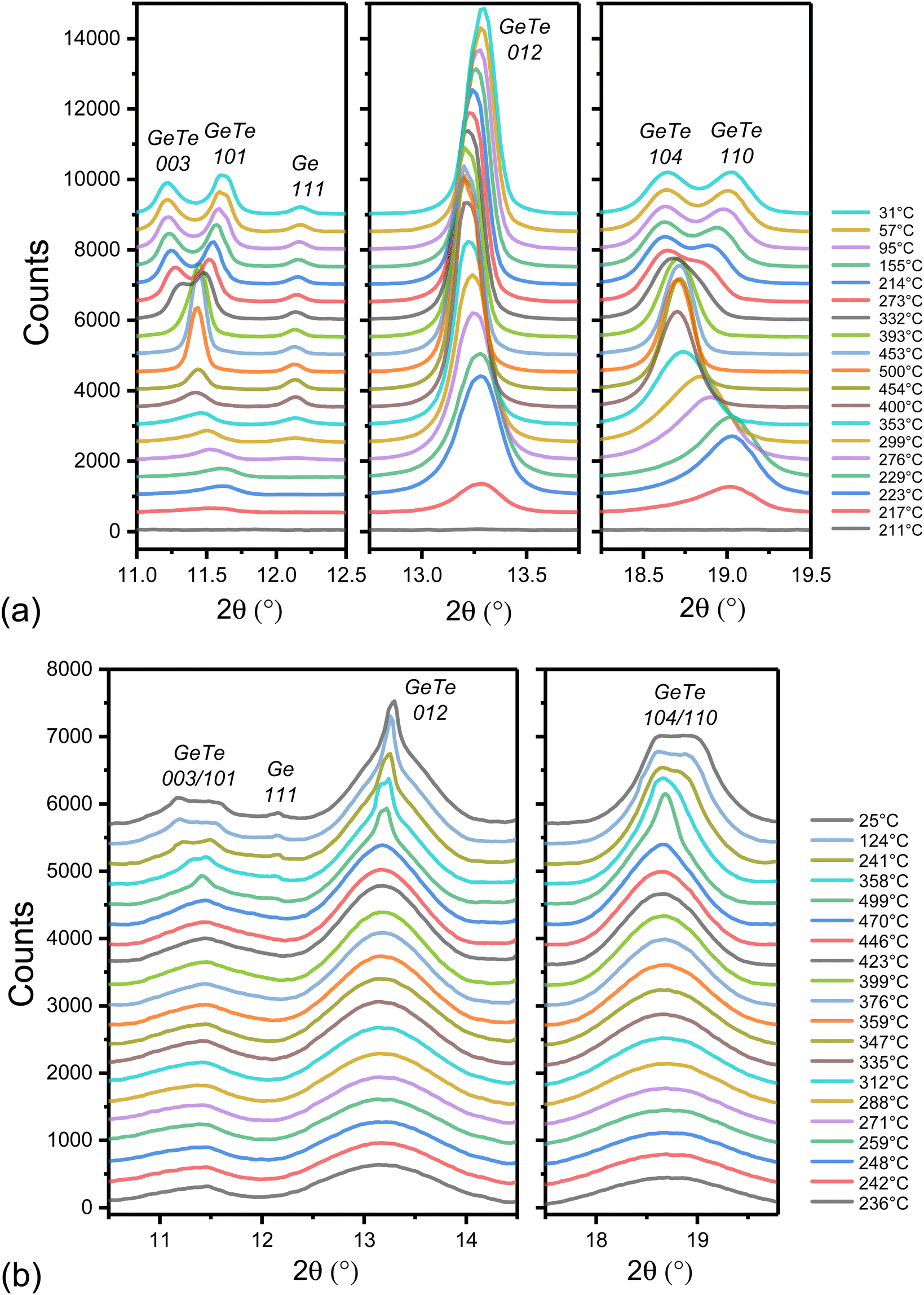 | ||
| Fig. 4 X-ray diffraction patterns (λ = 0.6908 Å, synchrotron radiation) at selected temperatures in the 2θ ranges of interest for the reference 50 nm thick GeTe film (a) and the [GeTe 4 nm/C 0.5 nm]22 ML film (b). For each diffraction pattern, a baseline has been subtracted. Vertical offsets between spectra, of 500 counts in (a) and 300 counts in (b), were used. The initially amorphous films were heated up to 500 °C at a rate of 2 °C min−1 and cooled down at a rate of 20 °C min−1. The GeTe diffraction peaks were indexed by using a multiple hexagonal unit cell. | ||
BF-STEM images of the [GeTe 4 nm/C 0.5 nm]22 film annealed at 300 °C are shown in Fig. 3(b) and (c). The annealing conditions (15 minutes at 300 °C) were chosen to mimic those encountered during integration into memory devices in our test vehicles.37 Alternating layers of GeTe and C are observed throughout the stack between the SiO2 substrate and the SiN capping layer, with well-defined interfaces between the GeTe and C layers. As expected from the Rs curve in Fig. 3(a), the GeTe layers are crystallized after annealing at 300 °C. Atomic planes within crystalline GeTe grains are detected in a magnified image (Fig. 3(c)). The thickness of the GeTe layers in the STEM images is close to the nominal thickness of 4 nm. A possible reduction in thickness induced by crystallization (≈7% in the case of a 100 nm thick GeTe film)50 cannot be detected within the accuracy of these STEM observations. BF-STEM image of the [GeTe 4 nm/C 1 nm]20 and [GeTe 4 nm/C 2 nm]17 films annealed at 300 °C also show a well-defined ML structure (Fig. S6, ESI†).
In order to study the structural changes in MLs as a function of temperature, temperature-resolved diffraction patterns were acquired by using synchrotron radiation. The diffraction patterns of the [GeTe 4 nm/C 0.5 nm]22 ML at selected temperatures are shown in Fig. 4 and compared to diffraction patterns measured in the same experimental conditions on a 50 nm thick GeTe film. Upon heating, diffraction peaks are detected at 217 °C in GeTe and 230 °C in [GeTe 4 nm/C 0.5 nm]22. These temperatures are slightly smaller than those deduced from the Rs drop in Fig. 3(a) because of the different heating rates (10 °C min−1 for Rs measurements and 2 °C min−1 for XRD). Diffraction rings are observed in the images acquired by the 2D detector, showing that the GeTe phase in the ML is polycrystalline, as it is in the GeTe film.
In the reference GeTe film (Fig. 4(a)), the peaks observed during cooling for T ≤ 393 °C can be unambiguously assigned to the rhombohedral α-GeTe phase (trigonal space group R3m). The 003/101 and 104/110 doublets characteristic of this phase are clearly observed in the 2θ ranges [11–12°] and [18–19.5°] and the 012 peak is observed at 2θ ≈ 13.3°. Peaks are indexed by using a hexagonal unit cell that contains 3 Ge and 3 Te atoms. The splitting between the diffraction angles of the two peaks of each doublet increases with decreasing temperature as expected.51–54 Asymmetric peaks are observed instead of doublets when heating from 217 °C to ≈430 °C. This is mainly due to the small size of the GeTe crystallites, which induces a significant broadening of the diffraction peaks. Above ≈430 °C, which is the temperature of the reversible transition between the rhombohedral α-GeTe phase and the cubic β-GeTe phase (fcc rock-salt type) in a Ge rich GeTe film,49 the 111, 200 and 220 peaks of the cubic GeTe phase are observed in Fig. 4(a). The α-GeTe phase can be described as a distorted fcc structure, in which the Ge and Te sublattices are displaced relative to each other in the [111] (or equivalent) direction of the initial cubic structure, resulting in the onset of a spontaneous electrical polarization in that direction. The relative displacement of Ge and Te sublattices decreases when the temperature increases and vanish at the rhombohedral–cubic transition.52,53,55
In the crystallized [GeTe 4 nm/C 0.5 nm]22 ML film, three broad diffraction peaks are observed in Fig. 4(b). The very large width of the diffraction peaks, resulting from the small size of the GeTe crystallites (see below), makes it impossible to detect the crystallization of the excess Ge, contrary to the case of the GeTe film where the 111 diffraction peak of Ge appears at 276 °C during heating as shown in Fig. 4(a). It also prevents the observation of the 003/101 and 104/110 doublets and thus the distinction between a cubic or rhombohedral structure of the GeTe layers in the ML. However, a comparison of diffraction patterns acquired at room temperature in out-of-plane and in-plane geometries on a [GeTe 4 nm/C 0.5 nm]22 ML previously crystallized by annealing at 425 °C (Fig. S7, ESI†) shows that the GeTe phase is rhombohedral at room temperature. The same conclusion applies to the [GeTe 4 nm/C 1 nm]20 and [GeTe 4 nm/C 2 nm]17 MLs.
The diffraction peak at 2θ ≈ 13.3° being a single peak at all temperatures (012 in the rhombohedral α-GeTe phase and 200 in the cubic β-GeTe phase), its full width at half maximum (FWHM) can be used to obtain the diffracting coherent domain (DCD) as a function of temperature (Fig. 5(a)). Details of the analysis are given in the ESI.† Under the experimental conditions, for 2θ ≈ 13.3° the angle between the normal to the diffracting planes and the normal to the film is 3.6°. The DCD value gives therefore information on the average size of the GeTe crystallites in the direction perpendicular to the GeTe layers. When the temperature exceeds 470 °C during heating, a narrow peak is detected, superimposed to the broad one present at lower temperature. It is also detected in all diffraction patterns measured during cooling (Fig. 4(b) and Fig. S8, ESI†). Its origin will be discussed below and the DCD values reported in Fig. 5(a) concern only the broad peak. The measured FWHM of the broad peak as a function of temperature is shown in Fig. S9 (ESI†). The possible contribution of inhomogeneous strains to the peak width can be safely neglected, the dominant contribution being due to the small crystallite size. The DCD value is found equal to 2.72 ± 0.1 nm at 236 °C. It increases with increasing temperature and reaches 4.5 ± 0.15 nm at 500 °C. Then, it remains constant during cooling. The rapid increase of the DCD value in the temperature range of 353–373 °C corresponds to the crystallization of excess Ge. This suggests that the formation of Ge crystallites, probably from an amorphous Ge phase located at the GeTe grain boundaries, releases stresses that limit the growth of GeTe crystallites. The same behavior is observed in the reference 50 nm thick GeTe film and in a 100 nm thick GeTe film.50 However, in these cases, the reduction of inhomogeneous strains during Ge crystallization also contributes to the reduction of the FWHM.50
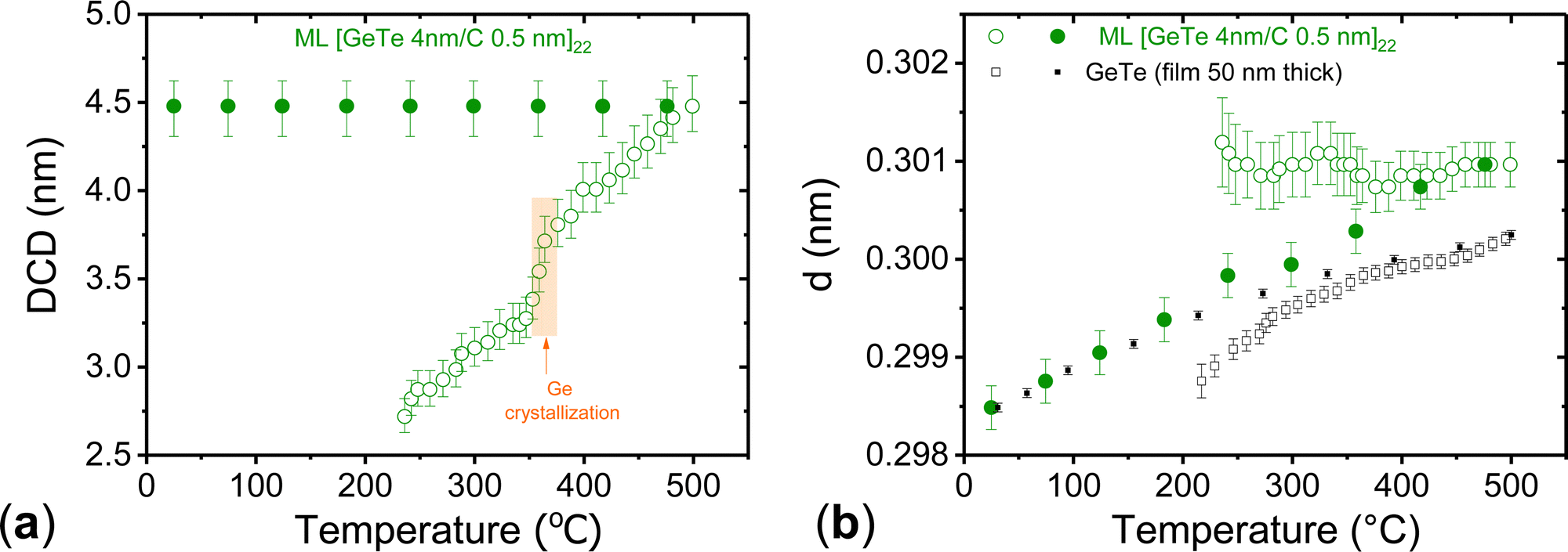 | ||
| Fig. 5 [GeTe 4 nm/C 0.5 nm]22 ML film. Temperature dependence of (a) the diffracting coherent domain (DCD) and (b) the interplanar spacing d of the diffraction peak at 2θ ≈ 13.3° (012 peak in the rhombohedral α-GeTe phase and 200 in the cubic β-GeTe phase) deduced from temperature-resolved XRD patterns (empty symbols: heating at 2 °C min−1, filled symbols: cooling at 20 °C min−1). For temperatures above 470 °C during heating and for all temperatures during cooling, the DCD and d values data are related to the broad diffraction peak (see text). In (b) the d values for the reference 50 nm thick GeTe film are shown for comparison. | ||
The existence of a narrow peak superimposed on the broad one reveals the formation of GeTe crystallites with a much larger size than those contributing to the broad peak. At a given temperature, the centers of the narrow and broad peaks are almost identical. The ratio of the integrated intensities of the narrow and broad peaks (≈8%) and the width of the two peaks remain constant during cooling down to room temperature (Fig. S8, ESI†). Thus, the nanostructure does not change during cooling. The DCD value deduced from the width of the narrow peak is equal to 30 ± 3 nm.
In summary, the above results show that a [GeTe 4 nm/C 0.5 nm]22 ML structure is maintained after being heated to 470 °C, a temperature well above the temperature limit tolerated by the back-end-of-line (BEOL) integration of microelectronics CMOS devices. The average size of GeTe crystallites in the direction perpendicular to the layers is 4.4 nm at 470 °C. Thus, 0.5 nm thick C layers are sufficient to limit the growth of GeTe grains in the direction perpendicular to the C layers and the crystallite size is only determined by the design of the amorphous ML structure as long as the annealing temperature is below 470 °C. Heating above 470 °C results in destruction of the [GeTe 4 nm/C 0.5 nm]22 ML structure at some locations with the formation of GeTe crystallites that have grown coherently through about 7 periods of the initial ML structure. However, the ML structure is retained in most of the film. Temperature-resolved XRD diffraction patterns of the [GeTe 4 nm/C 1 nm]20 were also acquired under the same experimental conditions. In this case, the ML structure remains stable up to 500 °C.
The temperature dependence of the interplanar spacing d, deduced from the center of the broad diffraction peak at 2θ ≈ 13.3° in Fig. 4(b) for the [GeTe 4 nm/C 0.5 nm]22 ML is shown in Fig. 5(b). It is compared with the d values for the reference 50 nm thick GeTe film. The d values measured in the ML during heating up to 500 °C and cooling differ strongly. During heating, d is almost temperature independent. By contrast, during cooling, d decreases when the temperature decreases. The d values measured during cooling below ≈200 °C in the ML and in the reference GeTe film coincide within the experimental accuracy. In this temperature range, the relative d changes are in agreement with those measured in GeTe polycrystalline ingots and in a GeTe single crystal,51,53,55,56 as shown in Fig. S10 (ESI†), and can therefore be entirely explained by the thermal expansion. The large differences between the d values measured in the ML at a given temperature during heating or cooling reveal the presence of stresses exerted by the C layers on the GeTe layers during heating. Differences between the d values measured upon heating and cooling also exist in the 50 nm thick GeTe film (Fig. 5(b)), as well as in a 100 nm thick GeTe film.50 However, in the GeTe films the d values measured upon heating are smaller than the d values measured during cooling. The opposite is observed in the ML. This major difference can be explained by the low thickness of GeTe layers in MLs combined with significant differences between the thermomechanical properties of GeTe and C layers. The volume thermal expansion of bulk rhombohedral α-GeTe is much larger than that of amorphous C films. The average linear thermal expansion coefficient is ≈1.9 × 10⁻⁵ K−1 from room temperature to 500 °C for GeTe.55,56 The expected value for sputtered C layers is ≈2.3 × 10⁻⁶ K−1.57 Stress effects exerted by the C layers on the GeTe ones could also be due to the high intrinsic compressive stress that is present in sputtered C films and can be released when annealing up to 500–600 °C.58 This explains why, after annealing the ML up to 500 °C and hence allowing release of the stress of C layers in the ML, the d values of the GeTe layers tend toward those of the GeTe film when cooling down from 200 °C to room-temperature (Fig. 5(b)).
3.3. Nanostructure of Ge2Sb2Te5 (GST)/C multilayers
The temperature-resolved sheet resistance curve of a [GST 4 nm/C 0.5 nm]22 ML is shown in Fig. 6(a) and compared to that measured on a reference 100 nm thick GST film. Upon heating, a drop in Rs of two orders of magnitude is observed at 168 °C in the GST film and at 180 °C in the ML. Similar curves were obtained in GST/C MLs with 9 nm thick GST layers in ref. 33. A BF-STEM image (Fig. 6(b)) of a [GST 4 nm/C 0.5 nm]22 ML film previously annealed at 300 °C shows a well-defined ML structure with bright C layers alternating with darker GST layers in which crystallized grains are visible. The interfaces between the GST and C layers are well defined throughout the entire ML, as shown by the HAADF-STEM image (Fig. 6(b)). Thus, in GST/C MLs, as in GeTe/C MLs, the ML structure is kept after crystallization of the phase-change material.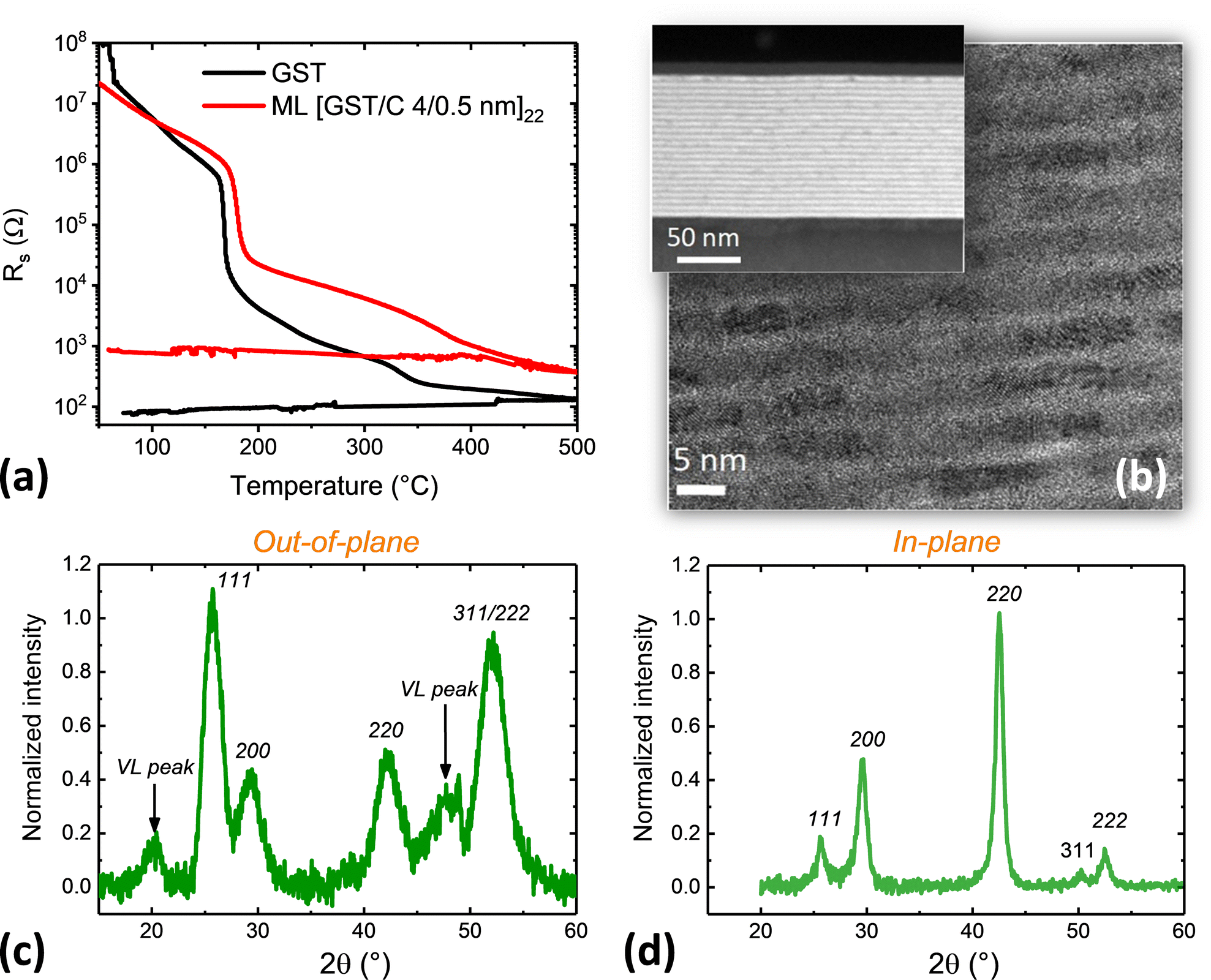 | ||
| Fig. 6 (a) Sheet resistance as a function of temperature when heating up to 500 °C and cooling (ramp rate of 10 °C min−1) for a 100 nm thick reference Ge2Sb2Te5 (GST) film and for a [GST 4 nm/C 0.5 nm]22 ML film. The as-deposited films are amorphous. The drop in resistance occurring at 168 °C in the GST film and 180 °C in the ML corresponds to the crystallization of GST. (b) BF-STEM image of a [GST 4 nm/C 0.5 nm]22 ML film crystallized by annealing at 300 °C for 15 minutes. Bright C layers alternate with darker GST layers in which crystallized grains are clearly visible. A HAADF-STEM image of the entire ML is shown in the inset. Bright GST layers and dark C layers with well-defined interfaces are visible throughout the image. (c) Out-of-plane and (d) in-plane room temperature diffraction patterns of a [GST 4 nm/C 0.5 nm]22 ML film annealed at 425 °C. Only cubic diffraction peaks are detected in the in-plane geometry. Additional diffraction peaks detected in the out-of-plane geometry reveal the reorganization of vacancies in vacancy layers (VLs). | ||
Upon further heating after crystallization of the GST layers, the sheet resistance steadily decreases as the temperature increases. This behaviour is similar to that observed in the GST film. In the latter case, it is explained by a progressive structural transition from the metastable fcc (rock salt type) phase, obtained after crystallization of the amorphous GST phase, to a stable trigonal phase. The metastable fcc phase contains a large amount of vacancies randomly distributed on the Ge/Sb sub-lattice. When the temperature increases, these vacancies migrate progressively in vacancy layers (VL).59–61 The structural reorganization ends up with the formation of the stable metallic trigonal structure where blocks of nine atomic planes terminated by Te planes are separated by pseudo van der Waals gaps.62
The structure of the [GST 4 nm/C 0.5 nm]22 ML annealed at 425 °C has been investigated by out-of-plane and in-plane XRD performed at room temperature (Fig. 6(c and d)). In-plane diffraction probes lattice planes that are nearly perpendicular to the film surface, while out-of-plane diffraction probes lattice planes that are parallel to the film surface. All diffraction peaks detected in the in-plane geometry can be indexed into a fcc structure. The cubic lattice parameter is equal to 0.6015 ± 0.0015 nm. This value is close to the one measured in crystallized GST films of a few hundred nm thickness.62 Cubic diffraction peaks are also detected in the out-of-plane geometry but two additional diffraction peaks are present. These peaks have been observed in GST films and are due to the existence of vacancy layers in the cubic structure.60 The absence of diffraction peaks due to vacancy layers in the in-plane diffraction pattern indicates that the atomic planes around the vacancy layers are preferentially parallel to the ML film surface. This is in agreement with observed changes in the relative area of the cubic diffraction peaks between the in-plane and out-of-plane geometries. The relative intensity of the 111 and 222 peaks is higher in the out-of-plane geometry. In the studied reference GST film the structural transformation is nearly complete after annealing at 425 °C. The out-of-plane diffraction pattern shows trigonal diffraction peaks, with weak subsisting VL type peaks. By contrast, in the [GST 4 nm/C 0.5 nm]22 ML, the structural transformation has just started at 425 °C. XRD patterns of [GST 4 nm/C 1 nm]20 and [GST 4 nm/C 2 nm]17 MLs lead to the same conclusion. DCD values of 3.6 nm in the direction normal to the GST layers are deduced from the width of the 200 cubic diffraction peak in the out-of-plane geometry for the [GST 4 nm/C 0.5 nm]22 ML. Note that in ref. 33, the large width of the diffraction peaks observed in crystallized GST/C MLs was erroneously attributed to the incorporation of C atoms in GST, whereas it must result, like in the presently studied MLs, from the limited height of the GST layers in the ML structure.
In summary, the GST/C ML structure is maintained by heating up to 425 °C and the structure of the GST phase remains cubic. The size of the GST crystallites in the direction normal to the layers is limited by the C layers and thus determined by the design of the amorphous ML structure.
4. Discussion
The above results show that depositing amorphous GeTe/C and GST/C MLs allows us to obtain by thermal treatment well defined stacks of crystallized GeTe or GST layers separated by amorphous C layers, even when the thickness of the C layer is only 0.5 nm. Direct proof of the amorphous character of the C layers is brought by Raman spectroscopy (see Fig. S11, ESI†). In the studied MLs, with a thickness of the deposited amorphous PCM layer equal to 4 nm, the average size of GeTe and GST crystallites in the direction normal to the layers is found to be limited by the C layers and thus determined by the ML design. Information on the average size of the crystallites in the plane of the layers can be obtained from the analysis of the width of the 012-diffraction peak in GeTe/C MLs, and the 200-diffraction peak in GST/C MLs, in the in-plane XRD patterns measured at room temperature on MLs previously annealed at 425 °C. The obtained DCD values are shown in Fig. 7 where they are compared to DCD values in the direction normal to the layers deduced from out-of-plane diffraction measurements on the same ML films. Details of the analysis are given in the ESI.†Fig. 7 shows that the shape of the GeTe crystallites in GeTe/C MLs is strongly anisotropic. Their average size in the plane of the layers is ≈30–45 nm, almost independent of the C layer thickness, to be compared to ≈3.5 nm in the direction perpendicular to the layers. The latter value differs slightly from that measured at 425 °C in the temperature-resolved XRD measurements due to the different annealing conditions. In GST/C MLs, the average size of the crystallites in the plane of the layers is ≈11–13 nm, almost independent of the C layer thickness. The striking difference in crystallite lateral size between GeTe/C and GST/C can be related to differences in the crystallization mechanisms of GeTe and GST amorphous films. In devices where a small amorphous volume is surrounded by a crystalline material, GeTe, as well as Ag–In–Sb–Te (AIST), behaves as a “growth-dominated” material and GST as a “nucleation-dominated” material.34 Differences are also observed between amorphous GeTe and GST thin films, for which the crystallization is induced by an annealing process.8,36 Once crystallization has been initiated, the crystallization in GeTe propagates from the existing crystalline parts, while in GST, the film crystallizes by further nucleation of new crystallites in the amorphous part of the film. As a result, the average crystallite size, after a given annealing ramp, is larger in GeTe films than in GST films.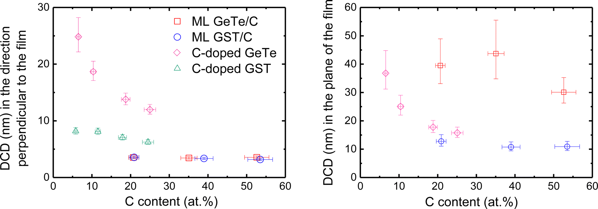 | ||
| Fig. 7 Diffracting coherent domain (DCD), deduced from room temperature XRD patterns, in the direction perpendicular to the film plane (left) and in the plane of the film (right) for GeTe/C and GST/C ML films and for C-doped GeTe and GST films previously annealed at 425 °C. The DCD gives information on the average size of the crystallites. The DCD values are plotted against the overall C content (at%) in the films which was calculated from the numbers of Ge, Te, Sb and C atoms measured using ion beam analysis techniques and reported in Table S2 (ESI†). | ||
The average crystallite sizes in MLs are compared in Fig. 7 to those measured in 100 nm thick C-doped GeTe and GST films with a C content between 5.8 and 25 at% crystallized using the same heat treatment as the MLs. The GeTe phase is rhombohedral in all the studied C-doped GeTe films (Fig. S7, ESI†). The average size of GeTe crystallites in C-doped GeTe films is almost the same in the direction normal to the film and in the film plane, in qualitative agreement with the STEM image in Fig. 2. For a given C content, the average size of GST crystallites is smaller than that of GeTe crystallites, which reflects the different crystallization mechanisms. In C-doped GeTe and GST films, the average size of crystallites decreases when the C content increases, as expected from literature results on similar films.2,7,20,23–25,42 In conclusion, strongly anisotropic crystallites in MLs and nearly isotropic crystallites in C-doped films with a C content larger than 18 at% have similar volumes but the ML structure allows a significant reduction in the size of crystallites in the direction perpendicular to the film, while allowing control of their interfaces. Smaller crystallite volumes are obtained in GST/C MLs than in GeTe/C MLs because of the nucleation-dominated character of GST. A ML structure allows investigation of the scaling effects on the crystallization of PCMs. For all MLs studied above, the thickness of the PCM layer was kept equal to 4 nm. In order to study the evolution of the crystallization temperature as a function of the nature of the stack, other GeTe/C and GST/C MLs were deposited, with a thickness of the PCM layers ranging from 2 to 19 nm. Their crystallization was studied by sheet resistance measurements (Fig. S4, ESI†). The crystallization temperatures (Tx) of all studied MLs are shown in Fig. 8. Similar trends are observed for GST/C and GeTe/C MLs, which excludes an influence of the excess of Ge in the case of GeTe/C MLs. When the thickness of the GeTe or GST layers is larger than 9 nm, Tx does not depend on the C layer thickness and coincides with Tx in the reference 100 nm thick films (≈230 °C for GeTe and ≈170 °C for GST). When the thickness of the GeTe or GST layer decreases below 9 nm, Tx increases. Even for GeTe layers as thin as 2 nm, the resistance drop at crystallization remains well-defined, with a large resistance contrast between the amorphous and crystallized state, as illustrated in the insert of Fig. 8(a). The same conclusion applies to the [GST 2 nm/C 1 nm]33 ML (Fig. 8(b)).
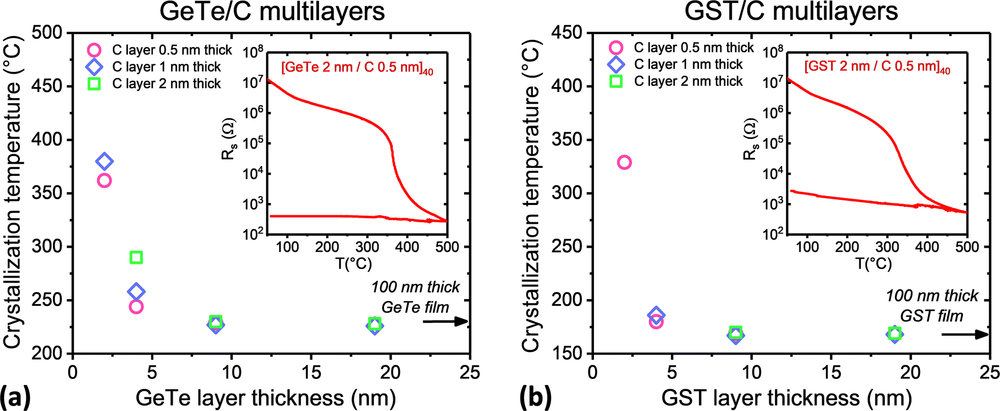 | ||
| Fig. 8 Crystallization temperature Tx of GeTe/C (a) and GST/C (b) MLs, deduced from sheet resistance measured during heating at a rate of 10 °C min−1, as a function of the nominal thickness of the deposited GeTe or GST layers. Tx is defined as the minimum of the derivative of the sheet resistance curve. Insets: Sheet resistance curves of the MLs with the smallest thickness of the PCM layers (2 nm). | ||
In the case of GeTe/C MLs, the effect of the C layer thickness on Tx could be studied. For 4 nm thick GeTe layers, Tx increases from 244 °C to 290 °C when the C layers thickness increases from 0.5 to 2 nm. Much stronger effects are observed when the GeTe layer is equal to 2 nm: Tx reaches 362 °C in a [GeTe 2 nm/C 0.5 nm]40 ML and 380 °C in a [GeTe 2 nm/C 1 nm]33 ML. The changes in Tx in GeTe/C MLs as a function of the thickness of the C and GeTe layers can be explained by scaling effects and by the stress exerted by the C layers onto the GeTe ones, with Tx increasing as the thickness of the C layers increases. In the case of GeTe thin films capped with a 10 nm thick SiN, decreasing the thickness under 20 nm results in an increase of Tx.1Tx reaches ≈300 °C in a 5 nm thick film. This large increase in Tx can be explained by the stress gradient exerted by the SiN capping layer on the GeTe layer. In the case of MLs, the stress exerted by the thin C layers on the GeTe layers is expected to be quite low compared to that induced by thicker and harder SiN layers, leading to a smaller increase in Tx.
5. Conclusion
The results presented show that a GeTe/C or GST/C ML structure allows fine control of the nanostructure of phase-change materials. Amorphous 0.5 nm thick C layers are sufficient to limit the growth of GeTe or GST grains in the direction perpendicular to the C layers. The crystallite size in the direction perpendicular to the layers is only determined by the design of the deposited ML. In GeTe/C MLs, the size of GeTe crystallites in the plane of the layers remains rather large (≈30–45 nm), which is a consequence of the growth-dominated-crystallization of GeTe. A much smaller lateral size (≈11–13 nm) is obtained in the case of GST/C MLs. Thus, the ML structure allows mastering the grain size and gets rid of the unavoidable variability of the nanostructure in C-doped PCMs.The ML nanostructure is retained after annealing at 425 °C, which allows integration of GeTe/C or GST/C MLs in memory devices with a full compatibility with the BEOL process. Such devices should benefit from the expected reduced thermal conductivity of the crystallized ML structure. This opens a promising perspective on the control of thermal confinement in phase-change memory devices, allowing to further limit energy waste upon programming, hence reducing the programming current. Indeed, we have recently succeeded in integrating a [GeTe 4 nm/C 1 nm]10 ML into phase-change memory test devices and have observed a significant improvement in programming performances.37 A reduction in the RESET current of about 55% and in drift coefficient of about 40% in ML devices annealed at 425 °C were observed in comparison with similar devices incorporating the Ge2Sb2Te5 reference PCM. Similar trends have been observed in devices based on GST/C MLs.33
Besides, the optical properties of GeTe are significantly modified in thin films made of crystalline GeTe nanoparticles (of about 5.8 nm in diameter) for which a decrease of the refractive index and extinction coefficient and an increase of the optical band gap are observed compared to the values for polycrystalline GeTe films.63 This beneficial effect for improving the material figure of merit in phase-change nano-photonic devices could be due to the quantum confinement effect or to the impact of the strong geometrical confinement on bonding properties due to the small size of the NPs. However, these types of NPs are not easily compatible with CMOS technology. The use of MLs allow benefitting from these properties in phase-change nano-photonic devices, opening promising perspectives.
Finally, such innovative ML nanostructures are of interest in other application areas. The GeTe phase, either pure or alloyed, with for instance Bi, Sb, or Pb, exhibits remarkable thermoelectric performances, as shown in many recent studies of bulk poly-crystals.10 These performances could be significantly improved in MLs thanks to the expected reduction of the thermal conductivity.
Author contributions
P. N. conceptualized the project on PCM nanocomposites, in close collaboration with V. M. G., and designed the experimental program. M. B. and R. C. prepared the thin film and multilayer samples in LETI clean rooms using industrial magnetron sputtering. P. N. acquired, curated and analysed the FTIR absorbance spectra of C-doped GeTe films. M. T. carried out the Raman spectroscopy of C-doped GeTe films with help from D. R. N. B. acquired, curated and analysed all the electron microscopy images (BF- and HAADF-STEM as well as EELS maps) under supervision of P. N. and with help from R. C. A. J. prepared all the high quality TEM foils. R. C. performed the 4-point probe resistance measurements as a function of temperature. M. T. J. P. and R. C. acquired, curated and analysed the laboratory XRD patterns. P. N., F. H. and C. M. performed the XRD experiments on the DiffABS beamline at SOLEIL synchrotron. F. H. curated and analysed all the XRD data. F. P. controlled the periodicity of the PCM/C ML samples by means of ToF-SIMS experiment and supervised the RBS/PIXE/NRA analysis of sample compositions performed at ARCANE (CENBG Gradignan). The paper was written by F. H. with review and editing from P. N. All authors have given their approval to the final version of the manuscript.Conflicts of interest
There are no conflicts to declare.Acknowledgements
We acknowledge SOLEIL for provision of the synchrotron radiation facilities (proposal 20181377) and we would like to thank all the staff at the DiffABS beamline for their assistance during the experiments. This research was partly funded by ANR under the contract MAPS ANR-20-CE05-0046-03 and from région AURA through “Pack Ambition recherche 2019 – Projet NANOCHARME”.Notes and references
- P. Noé, C. Vallée, F. Hippert, F. Fillot and J.-Y. Raty, Phase-change memories: materials science, technological applications and perspectives, Semicond. Sci. Technol., 2018, 33, 013002 CrossRef.
- Phase Change Memory, Device Physics, Reliability and Applications, ed. A. Redaelli, Springer, Cham, Switzerland, 2018 Search PubMed.
- P. Noé, A. Verdy, F. d’Acapito, J.-B. Dory, M. Bernard, G. Navarro, J.-B. Jager, J. Gaudin and J.-Y. Raty, Toward ultimate nonvolatile resistive memories: the mechanism behind ovonic threshold switching revealed, Sci. Adv., 2020, 6, eaay2830 CrossRef PubMed.
- T. Kim, H. Choi, M. Kim, J. Yi, D. Kim, S. Cho, H. Lee, C. Hwang, E.-R. Hwang, J. Song, S. Chae, Y. Chun and J.-K. Kim, High-performance, cost-effective 2z nm two-deck cross-point memory integrated by self-align scheme for 128 Gb SCM, 2018 IEEE International Electron Devices Meeting (IEDM), 2018, pp. 37.1.1–37.1.4.
- P. Fantini, Phase change memory applications: the history, the present and the future, J. Phys. D: Appl. Phys., 2020, 53, 283002 CrossRef CAS.
- S. R. Nandakumar, M. Le Gallo, I. Boybat, B. Rajendran, A. Sebastian and E. Eleftheriou, A phase-change memory model for neuromorphic computing, J. Appl. Phys., 2018, 124, 152135 CrossRef.
- G. Betti Beneventi, L. Perniola, V. Sousa, E. Gourvest, S. Maitrejean, J.-C. Bastien, A. Bastard, B. Hyot, A. Fargeix, C. Jahan, J.-F. Nodin, A. Persico, A. Fantini, D. Blachier, A. Toffoli, S. Loubriat, A. Roule, S. Lhostis, H. Feldis, G. Reimbold, T. Billon, B. De Salvo, L. Larcher, P. Pavan, D. Bensahel, P. Mazoyer, R. Annunziata, P. Zuliani and F. Boulanger, Carbon-doped GeTe: a promising material for Phase-Change Memories, Solid-State Electron., 2011, 65–66, 197–204 CrossRef CAS.
- P. Noé, C. Sabbione, N. Bernier, N. Castellani, F. Fillot and F. Hippert, Impact of interfaces on scenario of crystallization of phase change materials, Acta Mater., 2016, 110, 142–148 CrossRef.
- R. M. Young, P. Borodulin, N. El-Hinnawy, A. Ezis, M. R. King, V. Luu and D. T. Nichols, Improvements in GeTe-based Phase Change RF Switches, in 2018 IEEE/MTT-S International Microwave Symposium – IMS, 2018, pp. 832–835.
- J. Li, X. Zhang, X. Wang, Z. Bu, L. Zheng, B. Zhou, F. Xiong, Y. Chen and Y. Pei, High-Performance GeTe Thermoelectrics in Both Rhombohedral and Cubic Phases, J. Am. Chem. Soc., 2018, 140, 16190–16197 CrossRef CAS PubMed.
- Q. Tian, W. Zhang, Z. Qin and G. Qin, New Optimization Perspective of Thermoelectric Properties Based on Rashba Spin Splitting: a mini review, Nanoscale, 2021, 13, 18032–18043 RSC.
- P. Martinez, I. Papagiannouli, D. Descamps, S. Petit, J. Marthelot, A. Lévy, B. Fabre, J.-B. Dory, N. Bernier, J.-Y. Raty, P. Noé and J. Gaudin, Laser generation of sub-micron wrinkles in a chalcogenide glass film as physical unclonable functions, Adv. Mater., 2020, 32, 2003032 CrossRef CAS PubMed.
- J. Wang, L. Wang and J. Liu, Overview of Phase-Change Materials Based Photonic Devices, IEEE Access, 2020, 8, 121211 Search PubMed.
- S. Varotto, L. Nessi and S. Cecchi, et al., Room-temperature ferroelectric switching of spin-to-charge conversion in germanium telluride, Nat. Electron., 2021, 4, 740–747 CrossRef CAS.
- S. V. Faleev and F. Léonard, Theory of enhancement of thermoelectric properties of materials with nanoinclusions, Phys. Rev. B: Condens. Matter Mater. Phys., 2008, 77, 214304 CrossRef.
- W. Xu, Y. Liu, B. Chen, D.-B. Liu, Y.-H. Lin and A. Marcelli, Nano-inclusions: a novel approach to tune the thermal conductivity of In2O3, Phys. Chem. Chem. Phys., 2013, 15, 17595–17600 RSC.
- D. G. Cahill, P. V. Braun, G. Chen, D. R. Clarke, S. Fan, K. E. Goodson, P. Keblinski, W. P. King, G. D. Mahan, A. Majumdar, H. J. Maris, S. R. Phillpot, E. Pop and L. Shi, Nanoscale thermal transport. II. 2003–2012, Appl. Phys. Rev., 2014, 1, 011305 Search PubMed.
- A. Tlili, Y.-M. Beltukov, P. Desmarchelier, S. Merabia and A. Tanguy, Enhancement and anticipation of the Ioffe–Regel crossover in amorphous/nanocrystalline composites, Nanoscale, 2019, 11, 21502 RSC.
- H. Luo, A. Gravouil, V. Giordano and A. Tanguy, Thermal Transport in a 2D Nanophononic Solid: Role of bi-Phasic Materials Properties on Acoustic Attenuation and Thermal Diffusivity, Nanomaterials, 2019, 9, 1471 CrossRef CAS PubMed.
- L. Perniola, P. Noé, Q. Hubert, S. Souiki, G. Ghezzi, G. Navarro, A. Cabrini, A. Persico, V. Delaye, D. Blachier, J.-P. Barnes, E. Henaff, M. Tessaire, E. Souchier, A. Roule, F. Fillot, J. Ferrand, A. Fargeix, F. Hippert, J.-Y. Raty, C. Jahan, V. Sousa, G. Torelli, S. Maitrejean, B. De Salvo and G. Reimbold, Ti Impact in C-doped Phase-Change Memories compliant to Pb-free soldering reflow, 2012 International Electron Devices Meeting, 2012, pp. 18.7.1–18.7.4.
- A. Fantini, V. Sousa, L. Perniola, E. Gourvest, J.-C. Bastien, S. Maitrejean, S. Braga, N. Pashkov, A. Bastard, B. Hyot, A. Roule, A. Persico, H. Feldis, C. Jahan, J.-F. Nodin, D. Blachier, A. Toffoli, G. Reimbold, F. Fillot, F. Pierre, R. Annunziata, D. Benshael, P. Mazoyer, C. Vallée, T. Billon, J. Hazart, B. De Salvo and F. Boulanger, N-doped GeTe as Performance Booster for Embedded Phase-Change Memories, 2010 International Electron Devices Meeting, 2010, pp. 29.1.1–29.1.4.
- Q. Hubert, C. Jahan, V. Sousa, L. Perniola, A. Kusiak, J.-L. Battaglia, P. Noé, M. Bernard, C. Sabbione, M. Tessaire, F. Pierre, P. Zuliani, R. Annunziata, G. Pananakakis and B. de Salvo, A new insight on IRESET reduction of carbon-doped GST based PCM, International Conference on Solid State Devices and Materials, 2013, pp. 550–551.
- X. Zhou, M. Xia, F. Rao, L. Wu, X. Li, Z. Song, S. Feng and H. Sun, Understanding Phase-Change Behaviors of Carbon-Doped Ge2Sb2Te5 for Phase-Change Memory Application, ACS Appl. Mater. Interfaces, 2014, 6, 14207–14214 CrossRef CAS PubMed.
- T. Li, J. Shen, L. Wu, Z. Song, S. Lv, D. Cai, S. Zhang, T. Guo, S. Song and M. Zhu, Atomic-Scale Observation of Carbon Distribution in High-Performance Carbon-Doped Ge2Sb2Te5 and Its Influence on Crystallization Behavior, J. Phys. Chem. C, 2019, 123, 13377–13384 CrossRef CAS.
- Y. Cheng, D. Cai, Y. Zheng, S. Yan, L. Wu, C. Li, W. Song, T. Xin, S. Lv, R. Huang, H. Lv, Z. Song and S. Feng, Microscopic Mechanism of Carbon-Dopant Manipulating Device Performance in CGeSbTe-Based Phase Change Random Access Memory, ACS Appl. Mater. Interfaces, 2020, 12, 23051–23059 CrossRef CAS PubMed.
- T. C. Chong, L. P. Shi, X. Q. Wei, R. Zhao, H. K. Lee, P. Yang and A. Y. Du, Crystalline Amorphous Semiconductor Superlattice, Phys. Rev. Lett., 2008, 100, 136101 CrossRef CAS PubMed.
- Y. Hu, T. Lai, C. Di and X. Yan, The coupling effect and phase transition behavior of multiple interfaces in GeTe/Sb superlattice-like films, J. Alloys Compd., 2021, 871, 159467 CrossRef CAS.
- Q. Yin, M. Wang, X. Xu, G. Yu and L. Chen, Electrical and Mechanical Properties Enhancement in Superlattice-Like GaSb/Ge2Sb2Te5 Phase Change Thin Films, Adv. Mater. Interfaces, 2021, 8, 2100405 CrossRef CAS.
- R. Liu, P. Wu, Z. He, J. Zhai, X. Liu and T. Lai, Study of crystallization and thermal stability of superlattice-like SnSb4–GeTe thin films, Thin Solid Films, 2017, 625, 11–16 CrossRef CAS.
- P. Kowalczyk, F. Hippert, N. Bernier, C. Mocuta, C. Sabbione, W. Batista-Pessoa and P. Noé, Impact of Stoichiometry on the Structure of van der Waals Layered GeTe/Sb2Te3 Superlattices used in Interfacial Phase-Change Memory (iPCM) Devices, Small, 2018, 1704514 CrossRef PubMed.
- B. J. Kooi and J. Momand, High Resolution Imaging of Chalcogenide Superlattices for Data Storage Applications: Progress and Prospects, Phys. Status Solidi RRL, 2019, 13, 1800562 CrossRef.
- J. Shen, S. Lv, X. Chen, T. Li, S. Zhang, Z. Song and M. Zhu, Thermal Barrier Phase Change Memory, ACS Appl. Mater. Interfaces, 2019, 11, 5336–5343 CrossRef CAS PubMed.
- L. Zheng, W. Song, S. Zhang, Z. Song, X. Zhu and S. Song, Designing artificial carbon clusters using Ge2Sb2Te5/C superlattice-like structure for phase change applications, J. Alloys Compd., 2021, 882, 160695 CrossRef CAS.
- Phase Change Materials, ed. S. Raoux and M. Wuttig, Springer, New York, 2009 Search PubMed.
- J. Kalb, F. Spaepen and M. Wuttig, Atomic force microscopy measurements of crystal nucleation and growth rates in thin films of amorphous Te alloys, Appl. Phys. Lett., 2004, 84, 5240–5242 CrossRef CAS.
- A. N. D. Kolb, N. Bernier, E. Robin, A. Benayad, J.-L. Rouvière, C. Sabbione and F. Hippert, and Pierre Noé, Understanding the Crystallization Behavior of Surface-Oxidized GeTe Thin Films for Phase-Change Memory Application, ACS Appl. Electron. Mater., 2019, 1, 701–710 CrossRef CAS.
- D. Térébénec, N. Bernier, N. Castellani, M. Bernard, J.-B. Jager, M. Tomelleri, J. Paterson, M.-C. Cyrille, N.-P. Tran, V. M. Giordano, F. Hippert and P. Noé, Innovative Nanocomposites for Low Power Phase-Change Memory: GeTe/C Multilayers, Phys. Status Solidi RRL, 2022, 2200054 CrossRef.
- P. Pangaud, S. Basolo, N. Boudet, J.-F. Bérar, B. Chantepie, P. Delpierre, B. Dinkespiler, S. Hustache, M. Menouni and C. Morel, XPAD3: a new photon counting chip for X-ray CT-scanner, Nucl. Instrum. Methods Phys. Res. A, 2007, 571, 321–324 CrossRef CAS.
- C. Mocuta, S. Stanescu, M. Gallard, A. Barbier, A. Dawiec, B. Kedjar, N. Leclercq and D. Thiaudiere, Fast X-ray reflectivity measurements using an X-ray pixel area detector at the DiffAbs beamline, Synchrotron SOLEIL, J. Synchrotron Rad., 2018, 25, 204–213 CrossRef CAS PubMed.
- G. Ghezzi, J.-Y. Raty, S. Maitrejean, A. Roule, E. Elkaim and F. Hippert, Effect of carbon doping on the structure of amorphous GeTe phase change material, Appl. Phys. Lett., 2011, 99, 151906 CrossRef.
- J.-Y. Raty, P. Noé, G. Ghezzi, S. Maîtrejean, C. Bichara and F. Hippert, Vibrational properties and stabilization mechanism of the amorphous phase of doped GeTe, Phys. Rev. B: Condens. Matter Mater. Phys., 2013, 88, 14203 CrossRef.
- A. Kusiak, J.-L. Battaglia, P. Noé, V. Sousa and F. Fillot, Thermal conductivity of carbon doped GeTe thin films in amorphous and crystalline state measured by modulated photo thermal radiometry, J. Phys.: Conf. Ser., 2016, 745, 032104 CrossRef.
- M. J. Polking, J. J. Urban, D. J. Milliron, H. Zheng, E. Chan, M. A. Caldwell, S. Raoux, C. F. Kisielowski, J. W. Ager, R. Ramesh and A. P. Alivisatos, Size-Dependent Polar Ordering in Colloidal GeTe Nanocrystals, Nano Lett., 2011, 11, 1147–1152 CrossRef CAS PubMed.
- A. H. Edwards, A. C. Pineda, P. A. Schultz, M. G. Martin, A. P. Thompson, H. P. Hjalmarson and C. J. Umrigar, Electronic structure of intrinsic defects in crystalline germanium telluride, Phys. Rev. B: Condens. Matter Mater. Phys., 2006, 73, 045210 CrossRef.
- A. C. Ferrari and J. Robertson, Interpretation of Raman spectra of disordered and amorphous carbon, Phys. Rev. B: Condens. Matter Mater. Phys., 2000, 61, 14095–14107 CrossRef CAS.
- O. L. Krivanek, M. F. Chisholm, V. Nicolosi, T. J. Pennycook, G. J. Corbin, N. Dellby, M. F. Murfitt, C. S. Own, Z. S. Szilagyi, M. P. Oxley, S. T. Pantelides and S. J. Pennycook, Atom-by-atom structural and chemical analysis by annular dark-field electron microscopy, Nature, 2010, 464, 571 CrossRef CAS PubMed.
- C. E. Bottani, C. Mantini, P. Milani, M. Manfredini, A. Stella, P. Tognini, P. Cheyssac and R. Kofman, Raman, optical-absorption, and transmission electron microscopy study of size effects in germanium quantum dots, Appl. Phys. Lett., 1996, 69, 2409–2411 CrossRef CAS.
- D. Bermejo and M. Cardona, Raman scattering in pure and hydrogenated amorphous germanium and silicon, J. Non-Cryst. Solids, 1979, 32, 405–419 CrossRef CAS.
- D. I. Bletskan, Phase equilibrium in the system AIV-BVI Part. II Systems Germanium-Chalcogen, J. Ovonic Res., 2005, 1, 53–60 Search PubMed.
- M. Gallard, M. Salah Amara, M. Putero, N. Burle, C. Guichet, S. Escoubas, M.-I. Richard, C. Mocuta, R. Chahine, M. Bernard, P. Kowalczyk, P. Noé and O. Thomas, New insights into thermomechanical behavior of GeTe thin films during Crystallization, Acta Mater., 2020, 191, 60–69 CrossRef CAS.
- E. M. Levin, M. F. Besser and R. Hanus, Electronic and thermal transport in GeTe: a versatile base for thermoelectric materials, J. Appl. Phys., 2013, 114, 083713 CrossRef.
- T. Chatterji, C. M. N. Kumar and U. D. Wdowik, Anomalous temperature-induced volume contraction in GeTe, Phys. Rev. B: Condens. Matter Mater. Phys., 2015, 91, 054110 CrossRef.
- X. Q. Tran, M. Hong, H. Maeno, Y. Kawami, T. Toriyama, K. Jack, Z. G. Chen, J. Zou, S. Matsumura and M. S. Dargusch, Real-time observation of the thermally-induced phase transformation in GeTe and its thermal expansion properties, Acta Mater., 2019, 165, 327–335 CrossRef CAS.
- A.-K. U. Michel, F. Donat, A. Siegfried, O. Yarema, H. Fang, M. Yarema, V. Wood, C. R. Müller and D. J. Norris, Phase transitions in germanium telluride nanoparticle phase-change materials studied by temperature-resolved x-ray diffraction, J. Appl. Phys., 2021, 129, 095102 CrossRef CAS.
- T. Chattopadhyay, J.-X. Boucherle and H. G. von Schnering, Neutron diffraction study on the structural phase transition in GeTe, J. Phys. C: Solid State Phys., 1987, 20, 1431–1440 CrossRef CAS.
- H. Wiedemeier and P. A. Siemers, The Thermal Expansion of GeS and GeTe, Z. für Anorg. Allg. Chem., 1977, 431, 299–304 CrossRef CAS.
- C. Wei and C. H. Chen, The effect of thermal and plastic mismatch on stress distribution in diamond like carbon film under different interlayer/substrate system, Diamond Relat. Mater., 2008, 17, 1534–1540 CrossRef CAS.
- J. Robertson, Diamond-like amorphous carbon, Mater. Sci. Eng., R, 2002, 37, 129–281 CrossRef.
- W. Zhang, A. Thiess, P. Zalden, R. Zeller, P. H. Dederichs, J.-Y. Raty, M. Wuttig, S. Blügel and R. Mazzarello, Role of vacancies in metal–insulator transitions of crystalline phase-change materials, Nat. Mater., 2012, 11, 952–956 CrossRef CAS PubMed.
- V. Bragaglia, F. Arciprete, W. Zhang, A. M. Mio, E. Zallo, K. Perumal, A. Giussani, S. Cecchi, J. E. Boschker, H. Riechert, S. Privitera, E. Rimini, R. Mazzarello and R. Calarco, Metal – Insulator Transition Driven by Vacancy Ordering in GeSbTe Phase Change Materials, Sci. Rep., 2016, 6, 23843 CrossRef CAS PubMed.
- A. Lotnyk, T. Dankwort, I. Hilmi, L. Kienleb and B. Rauschenbach, In situ observations of the reversible vacancy ordering process in van der Waals-bonded Ge–Sb–Te thin films and GeTe–Sb2Te3 superlattices, Nanoscale, 2019, 11, 10838 RSC.
- T. Matsunaga, N. Yamada and Y. Kubota, Structures of stable and metastable Ge2Sb2Te5, an intermetallic compound in GeTe–Sb2Te3 pseudo-binary systems, Acta Crystallogr., Sect. B: Struct. Sci., 2004, B60, 685–691 CrossRef CAS PubMed.
- A.-K. U. Michel, M. Sousa, M. Yarema, O. Yarema, V. Ovuka, N. Lassaline, V. Wood and D. J. Norris, Optical Properties of Amorphous and Crystalline GeTe Nanoparticle Thin Films: A Phase-Change Material for Tunable Photonics, ACS Appl. Nano Mater., 2020, 3, 4314–4320 CrossRef CAS.
Footnote |
| † Electronic supplementary information (ESI) available. See DOI: https://doi.org/10.1039/d2tc03567g |
| This journal is © The Royal Society of Chemistry 2023 |