 Open Access Article
Creative Commons Attribution 3.0 Unported Licence
AlN interlayer-induced reduction of dislocation density in the AlGaN epilayer†
David Maria
Tobaldi
 *a,
Luc
Lajaunie
 bc,
Arianna
Cretì
d,
Massimo
Cuscunà
a,
Iolena
Tarantini
e,
Marco
Esposito
 a,
Gianluca
Balestra
ae,
Mauro
Lomascolo
d,
Adriana
Passaseo
a and
Vittorianna
Tasco‡
 a
a
aCNR NANOTEC Institute of Nanotechnology, Via Monteroni, Lecce 73100, Italy. E-mail: david.tobaldi@nanotec.cnr.it
bDepartamento de Ciencia de los Materiales e Ingeniería Metalúrgica y Química Inorgánica, Facultad de Ciencias, Universidad de Cádiz, Campus Río San Pedro S/N, Puerto Real, 11510, Cádiz, Spain
cInstituto Universitario de Investigación de Microscopía Electrónica y Materiales (IMEYMAT), Facultad de Ciencias, Universidad de Cádiz, Campus Río San Pedro S/N, Puerto Real, 11510, Cádiz, Spain
dInstitute for Microelectronic and Microsystems, CNR-IMM, Lecce 73100, Italy
eDepartment of Mathematics and Physics “Ennio De Giorgi”, University of Salento, c/o Campus Ecotekne, Via Monteroni, 73100, Lecce, Italy
First published on 16th April 2024
Abstract
The emerging ultrawide-bandgap AlGaN alloy system holds promise for the development of advanced materials in the next generation of power semiconductor and UV optoelectronic devices. Within this context, heterostructures based on III-nitrides are very popular in view of their applications as electronic and optoelectronic components. AlGaN-based deep UV emitters are gaining visibility due to their disinfection capabilities. Likewise, high electron mobility transistors are attracting increasing attention owing to their superior electron transport which yields high-speed and high-power applications. These devices are conventionally made of AlGaN/GaN heterostructures grown on foreign substrates. However, structural defects, including stress induced by a mismatch in unit cell parameters and the presence of dislocations, can not only decrease the efficiency of the light emitters (by facilitating the non-radiative recombination of electron–hole pairs), but also impede electron mobility within the two-dimensional electron gas at the AlGaN/GaN interface. Therefore, the significance of obtaining high-quality AlGaN layers becomes evident. Including a thin AlN interlayer between the GaN buffer layer and AlGaN is a possible answer to address these drawbacks. Not only do we show that a thin AlN layer, approximately ≤3 nm in thickness, between the GaN buffer and AlGaN layers, is effective in decreasing the dislocation densities in the AlGaN layer by around 30%, but also this is responsible for an increase in the electron mobility (approximately 33%) compared to a classical AlGaN/GaN heterostructure. Additionally, the resulting heterostructure exhibits better optical quality, with a 7-fold increase in intensity as well as a 20% reduction in full-width at half-maximum in the AlGaN emission.
1. Introduction
Group III-nitride semiconductor materials have a long-standing history of technological interest, finding applications ranging from optoelectronic to electronic devices.1 Not only the growth of the AlGaN compound has received extensive attention driven by its promising applications in deep-ultraviolet optoelectronic devices,2 as they cover the 200 to 365 nm region,3 but AlGaN/GaN-based devices are also particularly attractive due to their application as high-power/high-frequency high-electron mobility transistors (HEMTs), which hold tremendous potential to contribute to the economic growth of the traditionally silicon-based semiconductor industry.4Deep ultraviolet light emitting diodes (LEDs) and HEMTs are conventionally grown by means of molecular beam epitaxy, or via metal–organic chemical vapour deposition (MOCVD) on foreign substrates. Combining materials with different bandgaps, like AlGaN and GaN, at the heterointerface generates a perpendicular electric field due to strong spontaneous and piezoelectric polarisation. This field enables the parallel flow of electrons along the interface, leading to the formation of a two-dimensional electron gas (2DEG).5 This results in high electron concentration and mobility.6 However, factors like stress in the crystal structure, dislocations, interface roughness, and alloy disorder scattering contribute to a reduction in electron mobility, impeding the electron injection toward the active region in AlGaN/GaN heterostructures.7,8 It has also been shown that barrier-accelerated interface recombination could arise as a significant contributor to carrier loss at the AlGaN/GaN interface, posing a potential limitation to the efficiency of nitride-based UV LEDs.9 To address this issue, incorporating an AlN interlayer between the AlGaN and GaN buffer layers (i.e., AlGaN/AlN/GaN) has been reported as a promising approach, enhancing not only the density of the 2DEG, but also the current injection efficiency into the emitter's active region.10,11
The observed increase in electron mobility can be attributed to the larger conduction band offset introduced by the AlN interlayer and the reduced structural disorder in the AlGaN ternary layer.12 Not only has the utilisation of an AlN interlayer been employed to improve the properties and quality of AlGaN/GaN HEMTs,12–17 but it is widespread too, enhancing the quality of GaN epilayers in GaN-based LED devices.10,18–20
Research about this topic is gaining momentum again.21–24 In recent studies, attention has been directed towards the local structure and ordering of Al atoms in thick AlGaN epilayers.25 However, to our surprise, the majority of this recent literature overlooks the defect state, specifically dislocation densities, in the AlGaN layer,21,22 which might give interesting answers about both the electrical and optical properties of the whole heterostructure.8 Thus, understanding the defect state within the AlGaN epilayer will aim to contribute to the current body of knowledge. In this work, AlGaN/AlN/GaN heterostructures were grown using MOCVD, incorporating extremely thin AlN interlayers (≤3 nm). This simplified heterostructure, related to a LED/HEMT configuration, allows for a focused exploration of the influence of the AlN interlayer on both structural and transport properties. The density of the dislocations in the AlGaN layer has been estimated using a method based on the Fourier analysis of high resolution X-ray diffraction (HR-XRD) data.26 Capacitance–voltage measurements were performed to assess the 2D electron density, while the transmission line model (TLM) technique was employed to estimate mobility and sheet resistance. Experimental results showed that a 3 nm thin AlN layer between the GaN buffer and AlGaN layers is effective in decreasing the dislocation densities in the latter layer. This also yields an increase in the mobility of the resulting heterostructure compared to a classical AlGaN/GaN heterostructure.
2. Experimental
2.1 Growth of GaN/AlGaN heterostructures
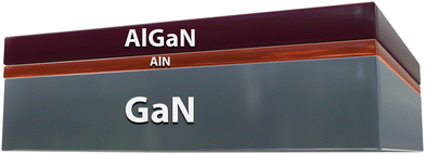
All epitaxial films employed in this study were grown directly on (00.1) c-plane Al2O3 substrates within a horizontal low-pressure MOCVD system (AIXTRON AlX 200-RF). The nitrogen, gallium, and aluminium precursors were NH3, trimethylgallium (TMGa), and trimethylaluminium (TMAl), respectively, with H2 serving as the carrier gas. The growth process commenced with the deposition of a 100 nm thick AlN nucleation layer directly onto an Al2O3 substrate at a temperature of 1180 °C.27 Subsequently, a 2 μm high-quality GaN buffer layer was grown. The following AlN interlayer (when present, with nominal thicknesses of 1.5 and 3 nm) and AlGaN epilayer of the heterostructure were then grown at the same temperature.28 A schematic of the epitaxial film structure is shown in Fig. 1. Specimens were labelled: A (no AlN interlayer), B (AlN interlayer = 1.5 nm), and C (AlN interlayer = 3 nm).2.2 Characterisation
The structural properties of the GaN/AlGaN heterostructures were investigated by means of HR-XRD, assessed on a Malvern PANalytical PW 3050/65 X'pert Pro MRD diffractometer (UK) with CuKα radiation (40 kV and 40 mA). To have information about the structural features of the prepared heterostructures, ω–2θ patterns and rocking curves (RCs) were recorded in a double-axis configuration, in parallel beam mode, using a parabolic mirror and a four bounce Ge (220) monochromator with the detector being kept at an open detector configuration. ω–2θ scan simulations were assessed with the X'Pert Epitaxy software package. To minimise effects due to wafer curvature, the beam height was restricted for symmetric RCs, whereas for skew symmetric ω-scans, the beam width was restricted, as suggested by Moram and Vickers.29 Quantitative information about the density of edge (ρedge), screw (ρscrew), and mixed (ρmixed = ρedge + ρscrew) dislocations in the GaN buffer as well as in the AlGaN layer was attained by collecting RCs along GaN/AlGaN asymmetric and symmetric reflections. To this aim, we employed the accurate method proposed by Kaganer et al.26 While the dislocation densities are commonly estimated via the full width at half maximum (FWHM) of a diffraction peak,29 the method proposed in ref. 26 assumes the line shape of the X-ray diffraction profiles of the epitaxial layers to be Gaussian only in the central most intense part of the reflection; the tails, instead, obey a power law decay, typically proportional to ω−3. Indeed, adopting the FWHM method, the tail regions of a reflection are totally neglected, neglecting thus the strain field in the near vicinity of a dislocation line.30 This latter method has also been shown to underestimate the dislocation densities.31 Besides, given the nanometric thickness of the AlGaN layer, asymmetric RCs were collected around its (12.3) reflection. The incidence angle ω of that reflection is around 0.67°, thus the contribution from the substrate is minimised, and a better resolution from the AlGaN signal can be obtained. Microstructural features were investigated by collecting reciprocal space maps (RSMs) around symmetrical (00.2), and asymmetrical (![[1 with combining macron]](https://www.rsc.org/images/entities/char_0031_0304.gif)
![[1 with combining macron]](https://www.rsc.org/images/entities/char_0031_0304.gif) .4) reflections. The Al content in the AlGaN layers was from HR-XRD RSM analyses.
.4) reflections. The Al content in the AlGaN layers was from HR-XRD RSM analyses.
Cathodoluminescence (CL) analysis was assessed at room temperature and in the 350–400 nm wavelength range, using a Zeiss SEM Merlin microscope equipped with a high-performance CL imaging system (SPARC from Delmic). CL was spectrally resolved with an Andor Kimera 193i spectrometer with a 193 mm focal length and a 150 gr mm−1 grating. The measurements were captured using an Andor Zyla5.5 CMOS camera with a maximum quantum efficiency of 60%, well-suited for visible spectroscopy. The electron beam was operated at an acceleration voltage of 5 kV, an emission current of 1 nA, and an integration time-per-pixel of 800 ms.
3. Results and discussion
3.1 HR-TEM microstructural analysis
The STEM analyses performed on the heterostructures A and C at low magnification are reported in the ESI,† Fig. S1–S3. Fig. 2 and 3 show the high-resolution STEM images and corresponding EDS maps of the AlGaN/GaN interfaces in the cases of samples A and C. Fig. 2a emphasises the well-defined and sharp interface between the AlGaN and GaN layers in heterostructure A. Conversely, a distinct dark and diffuse contrast is observed at the AlGaN/GaN interface (indicated by blue arrows in Fig. 3a), indicating the presence of the thin interlayer. EDS analyses were performed to gain further insight into its composition. The EDS maps and intensity profiles (Fig. 3b and S4,† respectively) reveal the presence of an AlN-rich interlayer, with an average thickness of 3 nm. Examination of these images suggests compositional fluctuations within the AlN interlayer, potentially contributing to the less sharply defined profile and interfaces. This observation suggests consideration of compositional pulling effects and/or Ga segregation within the AlN layer.32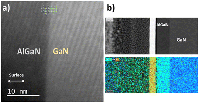 | ||
| Fig. 2 (S)TEM analyses of heterostructure A: a) high-resolution STEM-HAADF image, b) (top) HAADF image of the surface, and (bottom) the corresponding EDS maps. Additionally, a 3D ball-and-stick rendering along the [10.0] direction, created using the VESTA software suite,33 is presented in a). The yellow layer observed in b) represents a protective coating of gold, with Pt/C layers (visible to its left) used during the sample preparation process. | ||
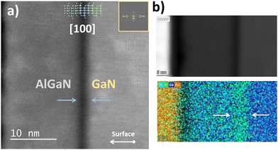 | ||
| Fig. 3 (S)TEM analyses of heterostructure C: a) high-resolution STEM-HAADF image, the blue arrows point to the AlN interlayer. b) (top) HAADF image of the surface and (bottom) the corresponding EDS maps. The white arrows highlight the AlN interfacial layer. In addition, a 3D ball-and-stick rendering along the [10.0] direction, created using the VESTA software suite,33 is shown in a). The inset in a) displays the fast Fourier transform pattern (obtained from the GaN buffer layer) described in the zone axis [10.0]. The yellow layer observed in b) represents a protective coating of gold (and Pt/C) used during the sample preparation process. | ||
3.2 XRR analysis
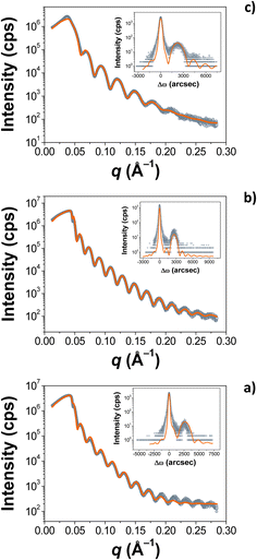
The thicknesses of the AlGaN layers, as well as those of the AlN interlayers, have been extracted by means of XRR. This technique is surface-sensitive: Kiessig fringes are uniquely caused by the interference of waves reflected at the surface of the layers.34 Therefore, deformations in the unit cell parameters do not have any influence on the resulting patterns. The XRR patterns of our heterostructures are displayed in Fig. 4, whilst data about the thicknesses are listed in Table 1. The thicknesses of the AlGaN layers were also estimated by analysing the RCs around the GaN/AlGaN (12.3) reflection (see the insets in Fig. 4, and the last column in Table 1). The fitting of XRR data indicates that the thicknesses of the AlN interlayers are consistent with their nominal values. Likewise, there is nice agreement (within the experimental error) between the thicknesses of the AlGaN layers extracted with XRR and those using RC (12.3) simulations, as shown in Table 1. Additionally, the XRR density of the AlN interlayer, as determined from the modelling, was found to be 3.0 ± 0.2 g cm−3 for heterostructure B and 3.1 ± 0.2 g cm−3 for heterostructure C. These values are slightly higher than the expected density for pure AlN (2.7 g cm−3). This difference suggests the presence of a small Ga mole fraction, estimated to be around 8–10%.| Heterostructure | XRR thickness (nm) | RC (12.3) thickness (nm) | |
|---|---|---|---|
| AlGaN | AlN interlayer | AlGaN | |
| C | 3.0 nm | 19.1 ± 0.1 | 2.9 ± 0.1 | 22 ± 3 |
| B | 1.5 nm | 28.9 ± 0.1 | 1.3 ± 0.1 | 30 ± 4 |
| A | 0 nm | 30.1 ± 0.1 | — | 29 ± 1 |
3.3 HR-XRD structural analysis
Fig. 5 displays the HR-XRD ω–2θ patterns, together with the simulations run considering the nominal thicknesses and compositional values. The GaN (00.4) reflection belonging to the buffer layer (positioned here at zero arcsec) and those belonging to the AlN nucleation layer (at around 6800 arcsec) and AlGaN are well visible. Pendellösung fringes can also be detected, being at the lower-angle side of the AlN reflection. Dislocation densities in the GaN buffer and in the AlGaN layers, as retrieved by the method proposed by Kaganer et al.,26 are listed in Table 2. For comparison, in the ESI† we also report the dislocation densities in the GaN and AlGaN epilayers, calculated using the commonly employed method that relies on the FWHM of ω scans.29 In that latter case, dislocation densities are undervalued of (at least) one order of magnitude compared to the method proposed in ref. 26 – this being consistent with our previous work.31 Nevertheless, similar conclusions can be drawn. One observation is that the quality of the GaN buffer layer is comparable in the three specimens, with the density of mixed dislocations being in the order of 1010 cm−2.27 Additionally, it is interesting to note that the densities of edge and mixed dislocations are quite similar, thus resembling a CVD growth method.35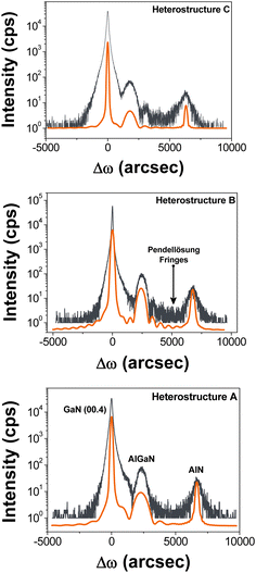 | ||
| Fig. 5 Collected (dark grey line) and simulated (orange line) HR-XRD (00.4) ω–2θ scans of the prepared heterostructures. From bottom to top: heterostructures A, B, and C. | ||
| Heterostructure | GaN | AlGaN | ||||
|---|---|---|---|---|---|---|
| ρ edge | ρ screw | ρ mixed | ρ edge | ρ screw | ρ mixed | |
| a The difference in GaN edge dislocation density across the samples may be due to inherent variations between the samples. However, considering the thickness of the GaN layer (∼2 μm) and the usual trend of decreasing dislocation density with greater thickness, we assume that these variations do not significantly affect the dislocation density in the uppermost layer(s). | ||||||
| C | 3.0 nm | 2.2 ± 0.2 | 0.2 ± 0.1 | 2.4 ± 0.2 | 0.9 | 0.3 | 1.1 |
| B | 1.5 nm | 1.6 ± 0.1 | 0.1 ± 0.1 | 1.7 ± 0.2 | 0.9 | 0.2 | 1.1 |
| A | 0 nm | 2.0 ± 0.2 | 0.1 ± 0.1 | 2.2 ± 0.2 | 1.2 | 0.3 | 1.5 |
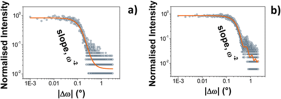
A different scenario can be drawn for the AlGaN epilayers. The dislocation density is higher in the sample without the AlN interlayer. Specifically, the edge dislocation density is reduced by about one-third (from 1.2 × 1010 cm−2 to 9 × 109 cm−2) with the presence of the AlN interlayer. This suggests a screening effect of the AlN interlayer, inhibiting the propagation of threading dislocations from the GaN buffer layer.36 Besides, consistent with a CVD growth method, the densities of edge and mixed dislocations in the AlGaN epilayer are comparable. This could account for the observed minimal change in screw dislocation density.35 It is also interesting to note that, for all of the samples, in the AlGaN layers the intensity distribution follows the ω−2 law (cf.Fig. 6), thus suggesting the finite thickness of the epitaxial layers to be the main source of the line broadening.26
The Al amount in the AlGaN layers has been calculated from the RSM (00.2) (Fig. 7a) by means of the technique proposed by Angerer et al.37 Results of HR-XRD RSM analyses are listed in Table 3. From the data reported in there, it is seen that the presence of the AlN interlayer led to a decrease in the stress status of the AlGaN layer. This effect is particularly noticeable in the heterostructure with a nominal 3 nm AlN interlayer – although it is worth noting that this very specimen contains a lower amount of Al in the AlGaN layer. As the thickness of the AlN interlayer varies, minimal changes are observed in the tilt of mosaic blocks constituting the epilayers (ranging from 3.6 to 7.2 arcsec; i.e., from 0.001° to 0.002°). Similarly, the influence of the AlN interlayer on the expansion of mosaic blocks in the lateral direction is found to be marginal, with no particular trend observed as the thickness of the AlN interlayer varies. The lateral expansion shifts from a minimum of 120 nm (sample A) to a maximum of 170 nm (sample B).
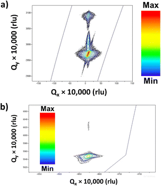 | ||
Fig. 7 a) RSM along the (00.2) reflection, heterostructure C. b) RSM along the (![[1 with combining macron]](https://www.rsc.org/images/entities/char_0031_0304.gif) ![[1 with combining macron]](https://www.rsc.org/images/entities/char_0031_0304.gif) 0.4) reflection, heterostructure C. 0.4) reflection, heterostructure C. | ||
| Heterostructure | Al (%) | ε ‖ (%) | ε ⊥ (%) | σ ‖ (GPa) | LCL (nm) | Mosaic spread (arcsec) |
|---|---|---|---|---|---|---|
| C | 3.0 nm | 24 | 0.36 | −0.06 | 1.66 | 130 | 7.2 |
| B | 1.5 nm | 30 | 0.90 | −0.19 | 4.20 | 170 | 3.6 |
| A | 0 nm | 29 | 0.92 | −0.29 | 4.29 | 120 | 3.6 |
3.4 Spectroscopic analysis: photoluminescence
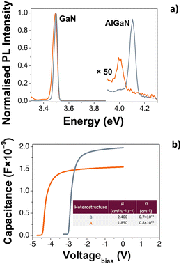
To evaluate the impact of the interlayer on the optical properties of the AlGaN layer, low-temperature PL measurements were recorded on the A and B heterostructures within the UV spectral range (Fig. 8a). In both the heterostructures, GaN PL emission (normalised in the figure) dominates the spectrum at about 3.50 eV, corresponding to free exciton ground and excited states.31 These bands show a typical asymmetric shape, originating from bandgap and excitonic complexes, in the sub-band gap, up to 3.30 eV. Additionally, in both the samples, a well-defined narrow band is also visible, with the maximum at about 4.00 eV and 4.10 eV, respectively, related to the AlGaN emission. The composition of AlGaN from these PL emissions aligns well with the XRD-estimated Al content (refer to Table S2†). In the heterostructure with the AlN layer (B), the intensity of the band gap emission in AlGaN is significantly greater than that in A, showing a seven-fold increase in the non-normalised scale. Additionally, the FWHM is reduced by approximately 20%, measuring 50 meV compared to 60 meV. These results suggest a better optical (structural) quality of the AlGaN material, due to the role of the AlN layer.3.5 Electrical measurement analyses
C–V profiles, measured at 20 kHz and obtained from the same specimens used for the PL analysis, are presented in Fig. 8b. A capacitance plateau, attributed to the 2DEG situated at the AlGaN/GaN interface, is evident in both heterostructures. The 2DEG density, determined through C–V measurements, was found to be 0.8 × 10¹³ and 0.7 × 1013 cm−2 for heterostructures A and B, respectively. These values align with the expected Al content, strain, and relaxation parameters inferred from XRD analysis for the undoped AlGaN barrier layer.39 Additionally, a pinch-off voltage of −3.0 V and −4.5 V is observed for heterostructures B and A (that without an AlN interlayer), respectively. The insertion of the AlN interlayer is likely responsible for the observed shift in the pinch-off voltage, attributable to the high dielectric constant ε0 of AlN.7 Moreover, the distinct defect density resulting from the inclusion of the AlN interlayer is evident in an enhanced 2DEG mobility, measured by TLM. In B, the mobility reaches approximately 2400 cm2 V−1 s−1, compared to the value of around 1850 cm2 V−1 s−1 observed in heterostructure A (inset of Fig. 8b). This confirms the advantageous impact of the AlN interlayer in reducing the dislocation density in the AlGaN epilayer, consequently enhancing the electrical properties of the resulting HEMT.Conclusions
AlGaN-based devices stand as highly promising materials for applications in deep ultraviolet optoelectronics and microelectronics. Nevertheless, achieving high-quality AlGaN poses considerable challenges. To address them, the integration of an AlN interlayer has emerged as a solution to enhance the structural integrity of AlGaN layers. HR-XRD, microstructural, and optical analyses revealed that the incorporation of a (nominal) ≤3 nm thick AlN interlayer between the GaN buffer layer and AlGaN results in halving the dislocation densities in the AlGaN layer. This decrease is attributed to the effective shielding to the threading dislocations provided by the AlN interlayer. The improved structural quality of the AlGaN epilayer not only enhances its overall quality, but also yields substantial improvements in the transport properties of the 2DEG at the GaN/AlGaN heterointerface in HEMT devices, as well as the radiative behaviour of AlGaN layers for UV applications. Results from this work hold promise for advancing the design and performance of high-quality III-nitride semiconductor devices, contributing to the ongoing progress in microelectronic and deep ultraviolet optoelectronic applications.Conflicts of interest
There are no conflicts to declare.Acknowledgements
The authors acknowledge financial support under the National Recovery and Resilience Plan (NRRP), Mission 4, Component 2, Investment 1.1, Call for tender No. 104 published on 2.2.2022 by the Italian Ministry of University and Research (MUR), funded by the European Union – NextGenerationEU – Project Title: Ultra-Thin Nitrides for Ultraviolet Lighting – IRIDE – CUP B53D23002890006 – Grant Assignment Decree No. 960 adopted on 30-06-2023 by the Italian Ministry of University and Research (MUR). This work was also partly supported by the Italian Ministry of Research (MUR) in the framework of the National Recovery and Resilience Plan (NRRP), “NFFA-DI” Grant (CUP B53C22004310006), and “I-PHOQS” Grant (CUP B53C22001750006) and under the complementary actions to the NRRP, “Fit4MedRob” Grant (PNC0000007, CUP B53C22006960001) and “ANTHEM” Grant (PNC0000003, CUP B53C22006710001), funded by NextGenerationEU. The authors also acknowledge the use of TEM instrumentation provided by the National Facility ELECMI ICTS (“Division de Microscopia Electronica”, Universidad de Cadiz, DME-UCA). Luc Lajaunie acknowledges funding from the Spanish Ministerio de Economía y Competitividad (PID2019-107578GA-I00, PID2022-140370NB-I00), the Ministerio de Ciencia e Innovación MCIN/AEI/10.13039/501100011033 and the European Union “NextGenerationEU”/PRTR (RYC2021-033764-I, CPP2021-008986).References
- O. Ambacher, J. Phys. D: Appl. Phys., 1998, 31, 2653–2710 CrossRef CAS.
- B. C. Letson, J. W. Conklin, P. Wass, S. Barke, G. Mueller, M. A. J. Rasel, A. Haque, S. J. Pearton and F. Ren, ECS J. Solid State Sci. Technol., 2023, 12, 066002 CrossRef.
- K. Jiang, X. Sun, J. Ben, Z. Shi, Y. Jia, Y. Wu, C. Kai, Y. Wang and D. Li, CrystEngComm, 2019, 21, 4864–4873 RSC.
- H. Amano, Y. Baines, E. Beam, M. Borga, T. Bouchet, P. R. Chalker, M. Charles, K. J. Chen, N. Chowdhury, R. Chu, C. D. Santi, M. M. D. Souza, S. Decoutere, L. D. Cioccio, B. Eckardt, T. Egawa, P. Fay, J. J. Freedsman, L. Guido, O. Häberlen, G. Haynes, T. Heckel, D. Hemakumara, P. Houston, J. Hu, M. Hua, Q. Huang, A. Huang, S. Jiang, H. Kawai, D. Kinzer, M. Kuball, A. Kumar, K. B. Lee, X. Li, D. Marcon, M. März, R. McCarthy, G. Meneghesso, M. Meneghini, E. Morvan, A. Nakajima, E. M. S. Narayanan, S. Oliver, T. Palacios, D. Piedra, M. Plissonnier, R. Reddy, M. Sun, I. Thayne, A. Torres, N. Trivellin, V. Unni, M. J. Uren, M. V. Hove, D. J. Wallis, J. Wang, J. Xie, S. Yagi, S. Yang, C. Youtsey, R. Yu, E. Zanoni, S. Zeltner and Y. Zhang, J. Phys. D: Appl. Phys., 2018, 51, 163001 CrossRef.
- S. Khandelwal, N. Goyal and T. A. Fjeldly, IEEE Trans. Electron Devices, 2011, 58, 3622–3625 CAS.
- M. J. Manfra, N. G. Weimann, J. W. P. Hsu, L. N. Pfeiffer, K. W. West, S. Syed, H. L. Stormer, W. Pan, D. V. Lang, S. N. G. Chu, G. Kowach, A. M. Sergent, J. Caissie, K. M. Molvar, L. J. Mahoney and R. J. Molnar, J. Appl. Phys., 2002, 92, 338–345 CrossRef CAS.
- O. Ambacher, J. Smart, J. R. Shealy, N. G. Weimann, K. Chu, M. Murphy, W. J. Schaff, L. F. Eastman, R. Dimitrov, L. Wittmer, M. Stutzmann, W. Rieger and J. Hilsenbeck, J. Appl. Phys., 1999, 85, 3222–3233 CrossRef CAS.
- M. Buffolo, A. Caria, F. Piva, N. Roccato, C. Casu, C. De Santi, N. Trivellin, G. Meneghesso, E. Zanoni and M. Meneghini, Phys. Status Solidi A, 2022, 219, 2100727 CrossRef CAS.
- Ž. Podlipskas, J. Jurkevičius, A. Kadys, S. Miasojedovas, T. Malinauskas and R. Aleksiejūnas, Sci. Rep., 2019, 9, 17346 CrossRef PubMed.
- J. Liu, J. Zhang, Q. Mao, X. Wu and F. Jiang, CrystEngComm, 2013, 15, 3372 RSC.
- W. Wang, Y. Li, Y. Zheng, Z. Yang, Z. Lin, X. Chen, Z. Lu and G. Li, CrystEngComm, 2018, 20, 4685–4693 RSC.
- S. Çörekçi, M. K. Öztürk, B. Akaoğlu, M. Çakmak, S. Özçelik and E. Özbay, J. Appl. Phys., 2007, 101, 123502 CrossRef.
- L. Shen, S. Heikman, B. Moran, R. Coffie, N.-Q. Zhang, D. Buttari, I. P. Smorchkova, S. Keller, S. P. DenBaars and U. K. Mishra, IEEE Electron Device Lett., 2001, 22, 457–459 CAS.
- C. Wang, X. Wang, G. Hu, J. Wang, H. Xiao and J. Li, J. Cryst. Growth, 2006, 289, 415–418 CrossRef CAS.
- L. Guo, X. Wang, C. Wang, H. Xiao, J. Ran, W. Luo, X. Wang, B. Wang, C. Fang and G. Hu, Microelectron. J., 2008, 39, 777–781 CrossRef CAS.
- A. Teke, S. Gökden, R. Tülek, J. H. Leach, Q. Fan, J. Xie, Ü. Özgür, H. Morkoç, S. B. Lisesivdin and E. Özbay, New J. Phys., 2009, 11, 063031 CrossRef.
- C. McAleese, M. J. Kappers, F. D. G. Rayment, P. Cherns and C. J. Humphreys, J. Cryst. Growth, 2004, 272, 475–480 CrossRef CAS.
- X.-Q. Shen, T. Takahashi, H. Matsuhata, T. Ide and M. Shimizu, CrystEngComm, 2015, 17, 5014–5018 RSC.
- Y. Lin, M. Yang, W. Wang, Z. Lin and G. Li, CrystEngComm, 2016, 18, 8926–8932 RSC.
- B. Tan, J. Hu, J. Zhang, Y. Zhang, H. Long, J. Chen, S. Du, J. Dai, C. Chen, J. Xu, F. Liu and X. Li, CrystEngComm, 2018, 20, 6557–6564 RSC.
- R. Ramesh, P. Arivazhagan, K. Prabakaran, S. Sanjay and K. Baskar, Mater. Chem. Phys., 2021, 259, 124003 CrossRef CAS.
- R. K. Kaneriya, C. Karmakar, G. Rastogi, M. R. Patel, R. B. Upadhyay, P. Kumar and A. N. Bhattacharya, Microelectron. Eng., 2022, 255, 111724 CrossRef CAS.
- K. Köhler, W. Pletschen, L. Kirste, S. Leone, S. Müller, R. Aidam, W. Bronner, P. Brückner, P. Waltereit, V. Polyakov and O. Ambacher, Semicond. Sci. Technol., 2022, 37, 025016 CrossRef.
- C. Piotrowicz, B. Mohamad, B. Rrustemi, N. Malbert, M. A. Jaud, W. Vandendaele, M. Charles and R. Gwoziecki, Solid-State Electron., 2022, 194, 108322 CrossRef CAS.
- A. Spindlberger, G. Ciatto, R. Adhikari, A.-K. Yadav and A. Bonanni, Appl. Phys. Lett., 2023, 123, 232101 CrossRef CAS.
- V. M. Kaganer, O. Brandt, A. Trampert and K. H. Ploog, Phys. Rev. B: Condens. Matter Mater. Phys., 2005, 72, 045423 CrossRef.
- V. Tasco, A. Campa, I. Tarantini, A. Passaseo, F. González-Posada, A. Redondo-Cubero, K. Lorenz, N. Franco and E. Muñoz, J. Appl. Phys., 2009, 105, 063510 CrossRef.
- A. Cretì, D. M. Tobaldi, M. Lomascolo, I. Tarantini, M. Esposito, A. Passaseo and V. Tasco, J. Phys. Chem. C, 2022, 126, 14727–14734 CrossRef.
- M. A. Moram and M. E. Vickers, Rep. Prog. Phys., 2009, 72, 036502 CrossRef.
- H. V. Stanchu, A. V. Kuchuk, Y. I. Mazur, C. Li, P. M. Lytvyn, M. Schmidbauer, Y. Maidaniuk, M. Benamara, M. E. Ware, Z. M. Wang and G. J. Salamo, Cryst. Growth Des., 2019, 19, 200–210 CrossRef CAS.
- D. M. Tobaldi, V. Triminì, A. Cretì, M. Lomascolo, S. Dicorato, M. Losurdo, A. Passaseo and V. Tasco, ACS Appl. Electron. Mater., 2021, 3, 5451–5458 CrossRef CAS.
- J. Houston Dycus, S. Washiyama, T. B. Eldred, Y. Guan, R. Kirste, S. Mita, Z. Sitar, R. Collazo and J. M. LeBeau, Appl. Phys. Lett., 2019, 114, 031602 CrossRef.
- K. Momma and F. Izumi, J. Appl. Crystallogr., 2008, 41, 653–658 CrossRef CAS.
- B. K. Tanner, in Handbook of Advanced Nondestructive Evaluation, ed. N. Ida and N. Meyendorf, Springer International Publishing, Cham, 2019, pp. 1181–1214 Search PubMed.
- V. M. Kaganer, B. Jenichen, M. Ramsteiner, U. Jahn, C. Hauswald, F. Grosse, S. Fernández-Garrido and O. Brandt, J. Phys. D: Appl. Phys., 2015, 48, 385105 CrossRef.
- Y. Chen, J. Ben, F. Xu, J. Li, Y. Chen, X. Sun and D. Li, Fundam. Res., 2021, 1, 717–734 CrossRef CAS.
- H. Angerer, D. Brunner, F. Freudenberg, O. Ambacher, M. Stutzmann, R. Höpler, T. Metzger, E. Born, G. Dollinger, A. Bergmaier, S. Karsch and H.-J. Körner, Appl. Phys. Lett., 1997, 71, 1504–1506 CrossRef CAS.
- D. J. Wallis, D. Zhu, F. Oehler, S. P. Westwater, A. Pujol and C. J. Humphreys, Semicond. Sci. Technol., 2013, 28, 094006 CrossRef CAS.
- O. Ambacher, B. Foutz, J. Smart, J. R. Shealy, N. G. Weimann, K. Chu, M. Murphy, A. J. Sierakowski, W. J. Schaff, L. F. Eastman, R. Dimitrov, A. Mitchell and M. Stutzmann, J. Appl. Phys., 2000, 87, 334–344 CrossRef CAS.
Footnotes |
| † Electronic supplementary information (ESI) available. See DOI: https://doi.org/10.1039/d4ce00191e |
| ‡ Vittorianna Tasco is currently seconded at the European Research Council Executive Agency of the European Commission. Her views expressed in this paper are purely those of the writer and may not in any circumstance be regarded as stating an official position of the European Commission. |
| This journal is © The Royal Society of Chemistry 2024 |

