
Twist angle and electric gating controllable electronic structure of the two-dimensional stacked BP homo-structure†
Linwei
Yao
a,
Jiangni
Yun
 *a,
Peng
Kang
b,
Hongyuan
Zhao
a,
Siyu
Zhang
a,
Liru
Zeng
a,
Zhisong
Bi
a,
Junfeng
Yan
a,
Wu
Zhao
a and
Zhiyong
Zhang
a
*a,
Peng
Kang
b,
Hongyuan
Zhao
a,
Siyu
Zhang
a,
Liru
Zeng
a,
Zhisong
Bi
a,
Junfeng
Yan
a,
Wu
Zhao
a and
Zhiyong
Zhang
a
aSchool of Information Science and Technology, Northwest University, Xian, 710127, China. E-mail: yjn_calculation@163.com; niniyun@nwu.edu.cn
bDepartment of Physics, McGill University, Montreal, Quebec H3A2T8, Canada
First published on 20th November 2023
Abstract
The boron phosphide (BP) van der Waals (vdW) homostructure is designed to construct high-performance nano-optoelectronic devices due to its distinctive photoelectric properties. Using density functional theory, the electronic properties of twisted and untwisted BP bilayer structures are systematically calculated. We found that the 0° structure is a direct band gap semiconductor with a type II band alignment, the carrier mobility of which is increased to 104, and its photoelectric conversion efficiency is 17.3%. By analyzing the band structure and exciton binding energy calculated at 0° under an electric field, it is further found that 0° is a superior photoelectric material. As for the twist BP bilayer, the band gap changes with torsional structures under the applied electric field, which generates the Stark effect. The twist angles of bilayer BP, specifically 13.17°, 21.79°, 38.21°, and 46.83°, always maintain a direct band gap under the influence of an electric field. While 60° is an indirect band gap, the structure exhibits high resistance to the electric field. Our results reveal that bilayer BP is a potential application prospect in photovoltaic and optoelectronic fields and can provide more insights into optoelectronic devices.
1 Introduction
In 2004, monolayer graphite (graphene) was successfully prepared through mechanical exfoliation, which paved the way for the research of two-dimensional (2D) materials. Until now, the bilayer vertical structure combining which is assembled through van der Waals (vdW) forces has attracted much attention. Bilayer structures with different stacking methods have distinct physical characteristics from monolayer structures,1 which has ignited enthusiasm for research. In the study of bilayer stacking sequences, numerous heterostructures have been discovered to possess favorable electronic structures, which are essential for the development of nanoscale devices in the future. In addition to strain engineering,2 halogenation,3 applied electric field (E⊥)4 and defects,5 moiré supercells are also used to control photoelectric devices in the study of bilayer 2D structures. Moiré supercells due to lattice mismatch usually occur in heterogeneous structures, while moiré supercells in homogeneous junctions occur due to different lattice orientations. In particular, the bilayer twisted vdW homostructure at different torsion angles exhibits remarkable properties, including Fermi velocity renormalization,6 new Van Hove singularities,7 Hofstadter's butterfly pattern,8 and unconventional quantum Hall effects.9 In addition to graphene, researchers also fabricated other 2D materials, such as twisted bilayer MoS2 (tb-MoS2),10 tb-MoSe2,11 tb-WSe2,12 and WSe2/WS2.13 In terms of theory, researchers explored the potential applications of twisted bilayer 2D materials in optoelectronic devices. They investigated the impact of the torsion angle on energy band regulation,14 Kagomé lattice,15 and strong correlations.16Recently, a graphene-like structure of 2D boron phosphorus (BP) has been demonstrated to have good mechanical stability, a moderate direct band gap, high carrier mobility, strong light absorption, and other advantages.17–19 This material is expected to be a candidate for the next generation of nano-electronics and optoelectronic applications. After Padavala et al.20 experimentally synthesized BP films with a wurtzite structure using chemical vapor deposition (CVD), several studies have been conducted on the optoelectronic properties of the BP heterojunction. Manish et al.21 found that the power conversion efficiency (PCE) of MoS2/BP heterojunction solar cells is much higher than that of MoS2/p-Si heterojunction solar cells. In addition, Joseph et al.22 found that changing the rotation angle between layers of the MoS2/BP heterostructure, and thus altering the type of band arrangement, can be not only useful for light-emitting diodes but also important for photovoltaic and photocatalytic applications. Khan et al.23 calculated the electron and optical properties of a BP/GaC heterojunction under specific strains by applying different strains, which is of great importance in the field of photovoltaic applications. In contrast to non-metallic materials, Mogulkoc et al.24 utilized black phosphorus and the BP heterostructure. This material exhibits strong light absorption in the ultraviolet region and low reflectivity in the visible region, making it suitable for transparent optoelectronic devices. It can be observed that the introduction of monolayer BP improves the photoelectric properties of the heterojunction system. However, there is a lattice mismatch between the two materials. Because the bilayer BP structure does not have the aforementioned issues, it presents a superior opportunity for studying bilayer BP. In these studies, E⊥ can change the Fermi energy level and charge redistribution, without chemical doping. Therefore, there have been some studies on bilayer BP, and Chen et al.25 have shown that the most stable bilayer BP stacks have direct band gaps and exhibit a significant Stark effect in the presence of E⊥. Furthermore, Wang et al.26 found that the band gap of bilayer BP is 1.098–1.312 eV, and its effective mass is approximately about times the rest mass of an electron (m0). Therefore, it has promising applications in the field of photoelectricity.
However, some key problems in the bilayer BP structure have not been studied. For example, the formation of moiré superlattices due to the torsion angle in the structure has been shown to greatly influence the electronic structure of the system.27–30 How does the torsion angle affect the interlayer interaction in bilayer BP? Furthermore, how do the torsion angle and E⊥ influence the band structure (BS) of bilayer BP? The in-depth research and exploration of bilayer BP will provide a fundamental understanding of vdW forces in a superimposed 2D structure. This understanding is of great significance for the development of BP devices. In this paper, we systematically study the effect of E⊥ on the photoelectric properties of bilayer BP with various twist angles. The results show that the engineering design of 2D layered materials using torsion angles is a promising and feasible method. This method has the potential to expand the applications of optoelectronics.
2 Computational methods
All calculations for bilayer BP are based on the density functional theory (DFT) first-principles CASTEP package and the plane-wave ultrasoft pseudopotential31 method. The generalized gradient approximation parameterized by the Perdew–Burke–Ernzerho (GGA–PBE) method32 is used to describe the electron exchange and correlation. Additionally, the van der Waals force (vdW) between the layers is corrected for using the Tkatchenko–Scheffler (TS) dispersion.33 The cutoff energy for the plane-wave basis is set to 500 eV. A Monkhorst–Pack special k-point method was used for the structural optimization calculation. The k-point grids used were 7 × 7 × 1, 5 × 5 × 1, and 3 × 3 × 1 for angles of 0° and 60°, 21.79° and 38.21°, and 13.17° and 46.83°, respectively. All geometries are fully relaxed until the convergence criteria for energies and forces are less than 10−5 eV and 0.02 eV Å−1. Dipole corrections were also considered in all calculations. To obtain more accurate electronic structures of various stacking structures, we utilized the Hyde–Scorselia Ernzerhof (HSE06) mixing function.34 However, in order to determine the variation trend of the energy band in the bilayer BP structure under the influence of E⊥, the PBE method is employed for calculation. Considering that the dielectric constant is jointly contributed by electrons and ions, the GW+BSE method of the VASP software package is adopted. The Brillouin zone (BZ) is sampled by 13 × 13 × 1, 9 × 9 × 1, 11 × 11 × 1, 11 × 11 × 1, 9 × 9 × 1, and 13 × 13 × 1 for electronic performance calculation of 0°, 13.17°, 21.79°, 38.21°, 46.83°, and 60°, respectively.To evaluate the stability of the stacking structure, it is determined by calculating Ef using the following formula,
| Ef = (Ebilayer − Etop − Ebottom)/n | (1) |
In addition, for the effect of interlayer vdW forces, we use the following formula,
| Eb = (Ebilayer − Etop+bottom)/S | (2) |
Using the average energy at 0° angle as the criterion, the relative average energy at other torsion angles is defined as,29
For charge transfer between bilayer BP, the in-plane differential charge density along the Z-axis is calculated using the following formula,
 | (3) |
The carrier mobility of bilayer BP is predicted using the transformation theory proposed by Bardeen and Shockley,35 and the formula is as follows:36
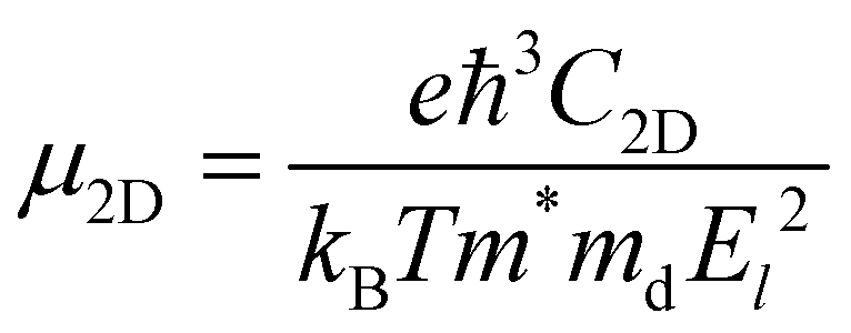 | (4) |
 . C2D is the in-plane elastic modulus, which can be derived from the formula (E − E0)/S0 = (C2D/2)(Δl/l0)2, where E0 and E are the total energies before and after applying uniaxial strain and S0 is the area of the optimized structure at the equilibrium state. E1 is the deformation potential constant, representing the change in band edges (CBM and VBM) after carriers are scattered by phonons, defined as E1= ∂Ed/∂δ, where Ed is the band edge energy.
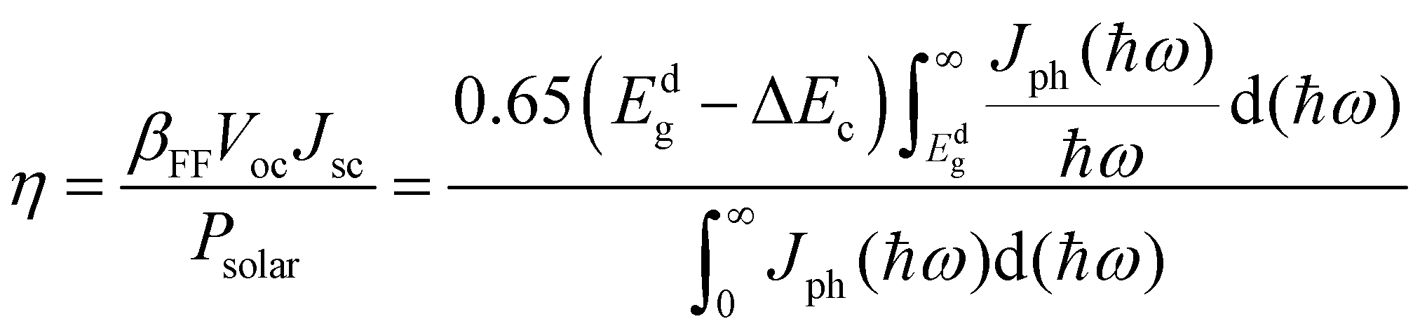
Using the upper power conversion efficiency limit established by Scharber et al.37 to calculate the power conversion efficiency (η) of the bilayer BP stack structure is shown below,
 | (5) |
The exciton binding energy (Eexc) in bilayer BP was calculated using the Wannier–Mott model,40 and the formula is as follows:
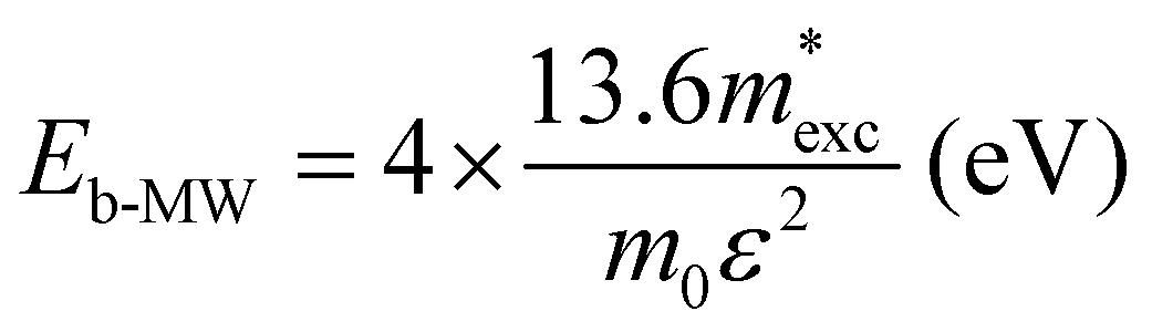 | (6) |
 is the exciton effective mass
 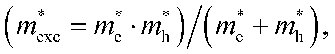 and
and  and
and  are the effective masses of electrons and holes, respectively. Table 3 shows the data of each parameter at the PBE level in detail.
3 Results and discussion
Before studying the bilayer, the accuracy of the structure was verified by examining the lattice constants of the optimized monolayer BP. The values obtained were a = b = 3.21, α = β = 90°, and γ = 120°, and the bond length of the B–P bond was found to be 1.847 Å. These results are consistent with previous theoretical findings (Table S1, ESI†).41 Using a 2 × 2 × 1 supercell monolayer of BP, the BS of the HSE06 method is calculated (Fig. S3(a), ESI†). The monolayer BP is a direct bandgap material with a band gap of 1.299 eV, which is in line with the findings of Wang et al.'s study.42 In addition, as can be seen from the skew wave density (DOS) and wave function distributions shown in Fig. 3(a), the valence band maximum (VBM) of the monolayer BP is contributed by the 3p orbital of the P atom, while the minimum conduction band (CBM) is contributed by the 2p orbitals of the B atom.3.1 Optimized structure and stability of the bilayer BP
The bilayer BP structure is composed of two monolayers stacked vertically. We constructed five highly symmetrical structures, as shown in Fig. S1, with specific stacking instructions given in the ESI.† Table S2 (ESI†) provides the interlayer spacing, formation energy (Ef), binding energy (Eb), and Eg values for the five stacking structures. It can be seen that the calculated distance between the layers is between 3.605 and 3.997 Å, which is significantly greater than the bond length between the atoms. The obtained interlayer forces range from −15.22 to 19.42 meV Å−2, which further confirms that there are only weak vdW forces between the layers.43 Fig. S2(a)–(c) (ESI†) shows the calculated data (Ef, Eb, and Eg) and interlayer distance under different stacking structures. According to the formation energy in Table 2, it can be concluded that the AB_B-P structure is the most stable. This conclusion is further supported by Fig. S2 (ESI†), which demonstrates the stability of the structure.Then, we define the AB_B-P structure as the initial structure with a torsion angle of 0°. The five selected twisted bilayer structures have no lattice mismatch, and their lattice constants are 14.004 Å, 8.500 Å, 14.004 Å, 8.500 Å, and 6.420 Å, corresponding to twist angles of 13.17°, 21.79°, 38.21°, 46.83°, and 60°, respectively, as shown in Fig. 1. Twist angle models were created using the builder interface in Virtual Nanolab (VNL).44Table 1 lists the interlayer spacing, Ef, Eb, ΔE, and Eg values and the number of structural atoms at different torsion angles. The sensitivity of the torsion angle at 60° is higher than that at 0°. The calculated Ef shows that the stability of the system decreases slightly after the introduction of a torsion angle between layers. We can assess the impact of the torsion angle change in the system's energy by calculating ΔE. When the torsion angle is 0°, ΔE is at its lowest, indicating that the system's stability is at its highest. For the interlayer forces of torsional structures, the calculated Eb values indicate that all interlayer forces are all vdW forces.
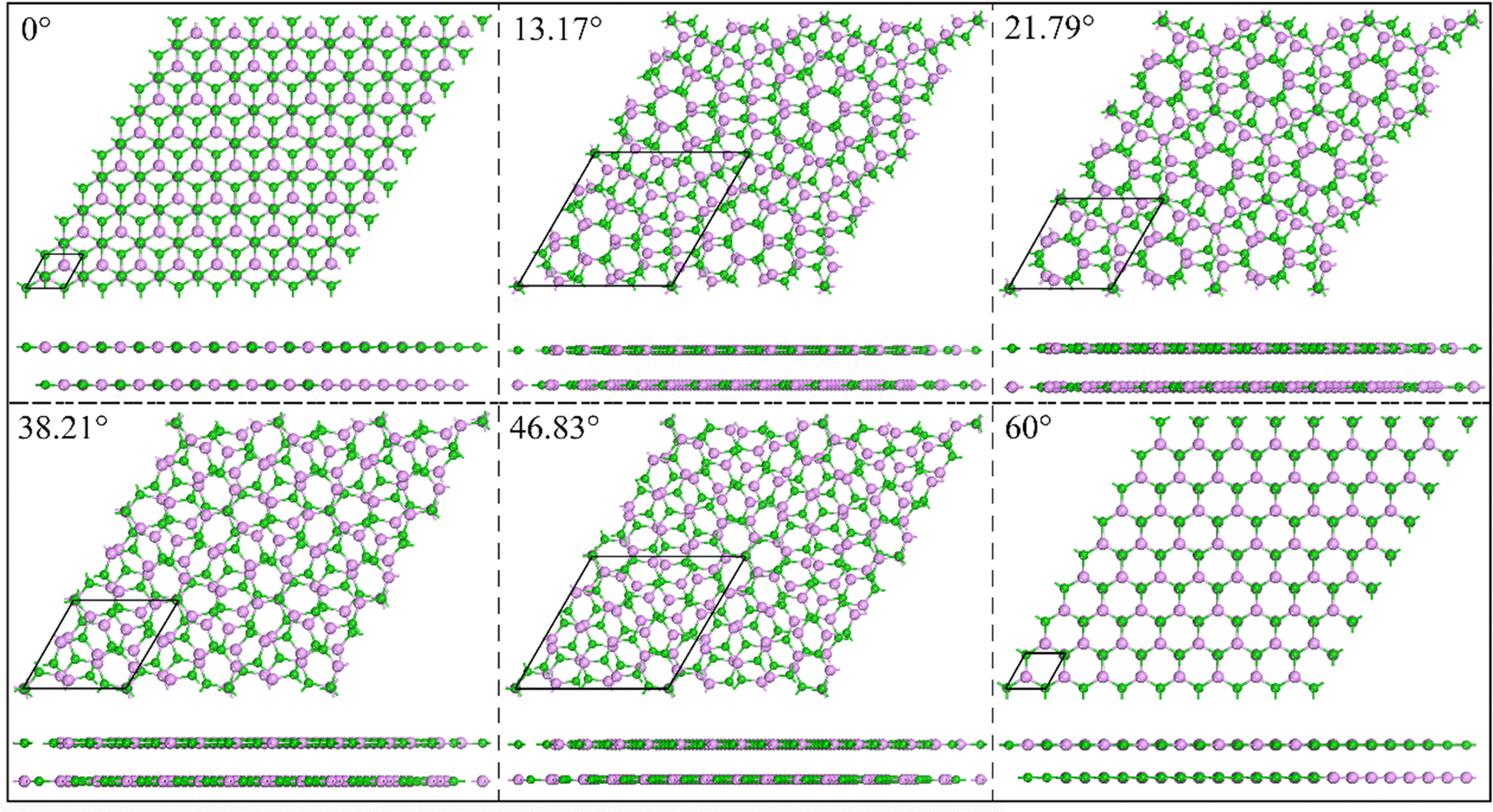 | ||
| Fig. 1 The top view and side view of BP under different torsion angles of 0°, 13.17°, 21.79°, 38.21°, 46.83° and 60°. The black rhombus lines represent basal cells. | ||
| θ | d (Å) | E f (meV per atom) | E b (meV Å−2) | ΔE (meV) | E g (eV) | N | Band type |
|---|---|---|---|---|---|---|---|
| 0° | 3.605 | −47.120 | −19.420 | 0.000 | 1.036(0.579) | 16 | Direct |
| 13.17° | 3.728 | −45.615 | −16.629 | 1.872 | 0.803(0.761) | 76 | Direct |
| 21.79° | 3.777 | −45.467 | −16.655 | 3.076 | 0.829(0.786) | 28 | Direct |
| 38.21° | 3.747 | −45.601 | −16.664 | 3.081 | 0.823(0.782) | 28 | Direct |
| 46.83° | 3.704 | −45.559 | −16.651 | 1.927 | 0.790(0.749) | 76 | Direct |
| 60° | 3.879 | −38.970 | −15.810 | 9.152 | 0.857(0.793) | 16 | Indirect |
3.2 Electronic structure of the bilayer BP
What are the properties of the different twist-angle structures? Then, we will examine their electronic structures. To analyze the electronic properties of the torsional structure in detail, Fig. 2 shows the BS and the partial wave density of states (PDOS) of the bilayer BP. The band gap values calculated using the HSE06 method are presented in Table 1. As depicted in Fig. 2, it can be observed that the band type remains a direct bandgap until the angle reaches 60°, after which it becomes an indirect bandgap due to band folding. Compared to the 0° structure, the band gaps of other twisted-angle structures not only decrease, but also the PDOSs of upper and lower BP layers are not separated. It can be concluded that the presence of a torsion angle alters the charge distribution between the layers, resulting in a different charge distribution in the upper and lower layers (Fig. S4, ESI†). For the 0° structure, we find that the VBM is provided by the top BP, and the CBM is provided by the bottom BP.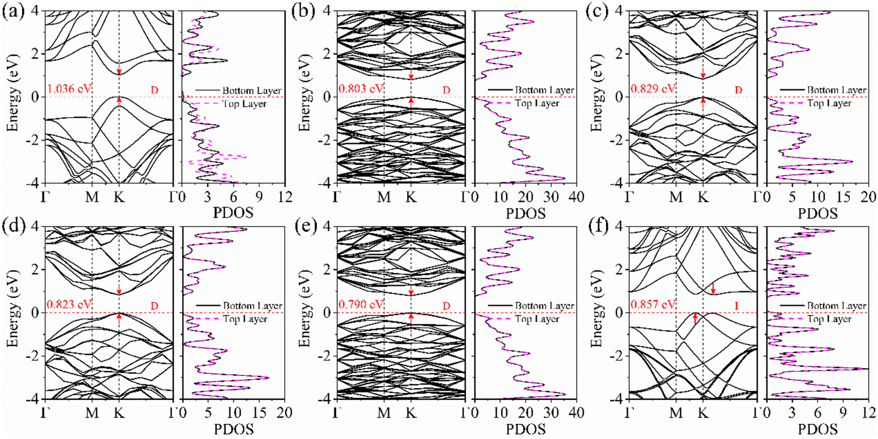 | ||
| Fig. 2 The BS and PDOS evolutions of bilayer BP at different twist angles of (a) 0°, (b) 13.17°, (c) 21.79°, (d) 38.21°, (e) 46.83°, and (f) 60°, respectively. | ||
Why does the most stable stacking structure exhibit different results compared to other structures, with charge separation between layers? Therefore, we further studied the distribution of the interlayer differential charge density and electrostatic potential in the 0° structure. The differential charge density calculated using formula (4) is shown in Fig. 3(a). A positive value of Δρ indicates the accumulation of electrons, while a negative value indicates the depletion of electrons at this position. Through analysis, it is found that the B atoms in the bottom layer transfer 0.04e to the P atoms in the top layer. Additionally, the electrostatic potential of the bottom layer is 0.28 eV higher than that of the top layer. These findings indicate the presence of a built-in electric field (Ein) between the layers, with the field direction being from the bottom layer to the top layer. For the generation of Ein, the symmetry of space inversion is broken because the mirror image of the 0° structure is not symmetric in the Z direction. The difference in electronegativity between the atoms results in the transfer of electrons from the bottom layer to the top layer. This is consistent with our results on the differential charge density and the distribution of the electrostatic potential. From the partial density of states (PDOS) in Fig. S3(d) (ESI†), it can be observed that the conduction band minimum (CBM) primarily originates from the bottom BP, while the valence band maximum (VBM) mainly originates from the top BP. This configuration results in a type II band alignment, which facilitates the efficient separation of photogenerated electron–hole pairs. The wave function distribution in Fig. S3(d) (ESI†) more vividly demonstrates the contribution of the CBM and VBM. In addition, the CB bias (CBO) and VB bias (VBO) of the AB_B-P structure are important indicators for separating electron–hole pairs. Larger VBOs or larger CBOs or both, help with separation. Fig. 3(b) shows that light can enhance the transfer process of photogenerated carriers. The CBO and VBO of the AB_B-P structure are 0.54 eV and 0.41 eV, respectively. These values are significantly higher than the thermal energy (0.026 eV) at room temperature. This indicates that the AB_B-P structure is capable of efficiently separating photogenerated carriers, which is crucial for 2D optoelectronic materials.
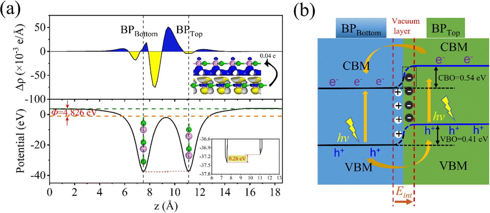 | ||
| Fig. 3 AB_B-P stacking structure: (a) differential charge integration and electrostatic potential distribution, and (b) band offset diagrams. | ||
For photovoltaic cells, the light absorption coefficient and carrier mobility of the material have a significant impact on photoelectric conversion. Therefore, we first calculated the optical absorption spectrum of monolayer BP, and the results were consistent with those of previous research.45 Then, the light absorption at 0° is calculated as shown in Fig. 4(a). It can be observed that the absorption at 0° is higher than that of the monolayer BP structure in the energy range of 1.63 to 4.00 eV. This is significant for improving the efficiency of solar cells. Carrier mobility is a crucial factor in facilitating high-performance electronics. Next, for a more intuitive description of the carrier transfer calculation, we construct a rectangular monolayer of BP with a structured unit cell at 0°, where the vectors x and y are aligned along the armchair and zigzag directions, respectively. The data calculated according to formula (5) are listed in Table 2 and Fig. S5, S6 (ESI†). The electron mobility of monolayer BP is as high as 104 cm2 V−1 s−1, which is more than twice the hole mobility. This finding is consistent with previous calculations.17 In the 0° structure, the electron mobility in the x- and y-directions reaches a high value of 23.12 × 103 cm2 V−1 s−1, while the hole mobility remains relatively unchanged compared to the monolayer. Significant differences in electron mobility and hole mobility hinder the recombination of photogenerated carriers, thus extending the lifetime of the carriers. Due to its strong deformation resistance and ability to suppress lattice vibrations in the bilayer stacking structure, the crystal exhibits a reduced number of phonons and electron–phonon scattering probability. This, in turn, enhances the performance of carrier transport. Fig. 4(b) shows a comparison of the mobility of the 0° structure with other 2D structures. It is found that the mobility of electrons and holes in the 0° structure is generally higher than that of other structures. Finally, we calculated the photoelectric conversion efficiency to be 17.3% using formula (6), as depicted in Fig. 4(c).
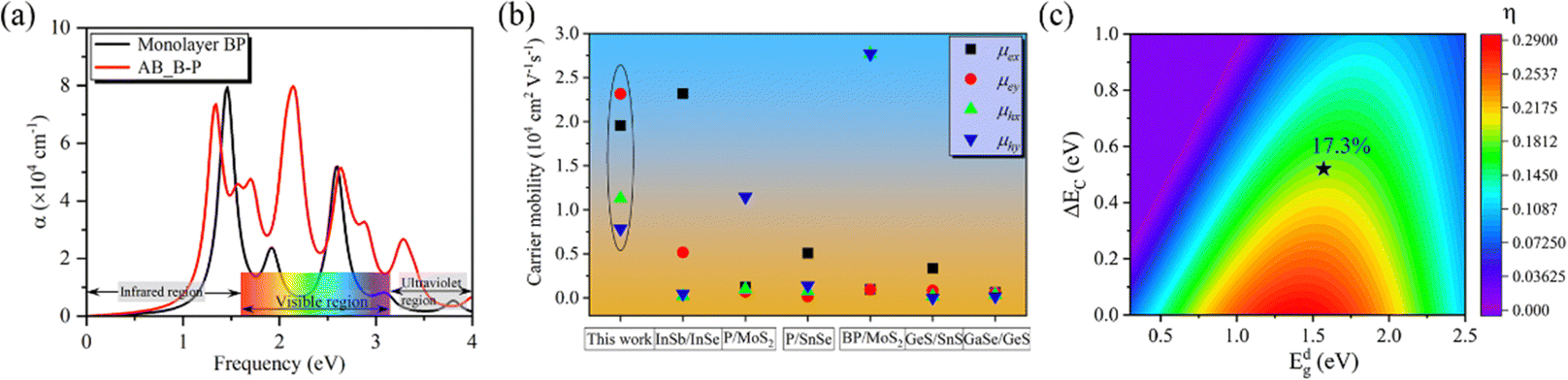 | ||
| Fig. 4 (a) The calculated optical absorption coefficient α of the monolayer and 0° structure, (b) carrier mobility for the 0° structure and other reported 2D heterostructures, and (c) solar energy conversion efficiency of 0° structure. | ||
| System | Carrier type | Direction | m* (m0) | E 1 (eV) | C 2D (J m−2) | μ (103 cm2 V−1 s−1) |
|---|---|---|---|---|---|---|
| Monolayer BP | Electron | Armchair | 0.300 | 1.78 | 185.54 | 17.93 |
| Zigzag | 0.172 | 1.77 | 189.61 | 18.53 | ||
| Hole | Armchair | 0.180 | 3.05 | 185.54 | 7.25 | |
| Zigzag | 0.187 | 3.14 | 189.61 | 6.99 | ||
| 0° structure | Eectron | Armchair | 0.526 | 1.48 | 370.55 | 19.56 |
| Zigzag | 0.248 | 1.36 | 371.31 | 23.12 | ||
| Hole | Armchair | 0.580 | 1.42 | 370.55 | 11.30 | |
| Zigzag | 0.434 | 1.69 | 371.31 | 7.86 | ||
3.3 Electric field control of bilayer BP electronic structure
Through previous studies, we have found that the 0° structure exhibits interlayer charge properties that differ from those of other torsional structures. The results also show that the structure performs well in photoelectric devices. The results show that E⊥ is of great value in adjusting the Eg of the 2D structure.46,47 Compared with the HSE06 method, the PBE method can conveniently obtain almost the same theoretical band trend (refer to Table 1 and Table S1, ESI†). Therefore, we use the PBE method to explore the electronic properties of the twisted BP structure under E⊥, which plays a significant role in guiding future experimental research. The direction of the electric field is shown in Fig. 5, where the positive direction of the vertical applied electric field is defined as the same as the direction of the Ein electric field from bottom to top. Otherwise, it is called the negative direction of the E⊥. The change in the Eg of the torsional structure with E⊥ is shown in Fig. 5. This clearly demonstrates that the Eg of the bilayer BP can be modified by E⊥. With the increase of E⊥ from −1.0 to 1.0 V Å−1, the Eg of the 0° structure gradually increases. The Eg evolution of other torsion angles is related to the strength of E⊥ and is inversely proportional to E⊥. This situation is mainly caused by the difference between E⊥ and the charge distribution across the layers. To provide a more detailed explanation of how E⊥ affects the electronic structure of the system, we have selected three specific angles −0°, 13.17°, and 60°, based on the varying coefficients of the giant Stark effect.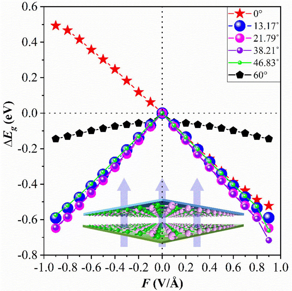 | ||
| Fig. 5 The bandgap variations of bilayer BP with different twist angles under the approach of E⊥. | ||
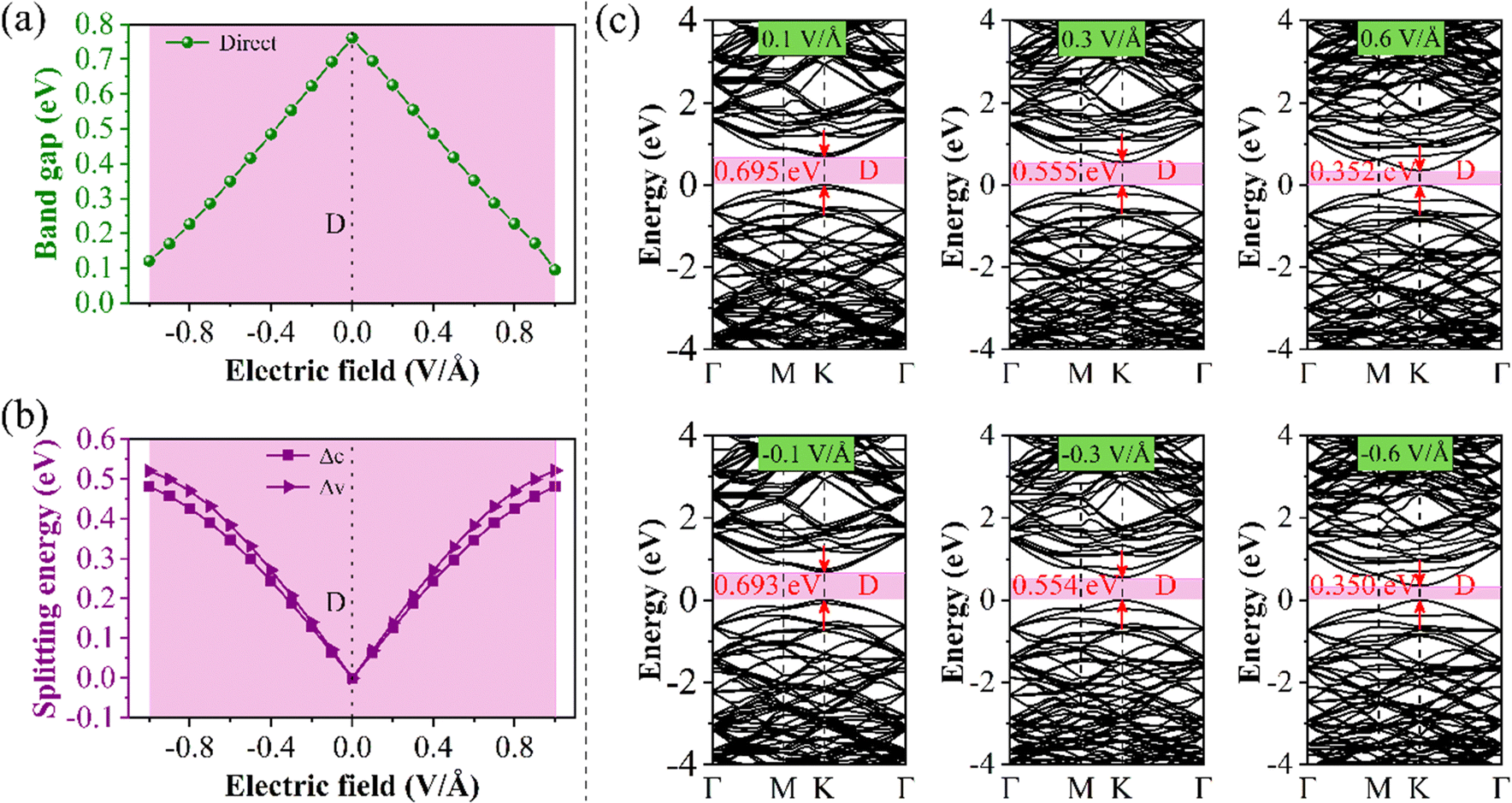
First, the evolution of the Eg of the 0° structure with E⊥ is shown in Fig. 6. From the BS, it can be seen that both the CBM and VBM have energy level splitting. We denote the splitting values at the CBM and the VBM as Δc and Δv, respectively. This clearly shows that Eg varies linearly with the electric field perpendicular to the material (E⊥). This indicates that the modulated electronic structure is primarily due to the Stark effect under E⊥. This effect can be observed in materials such as MoS2, WSe2, and graphene.48–50
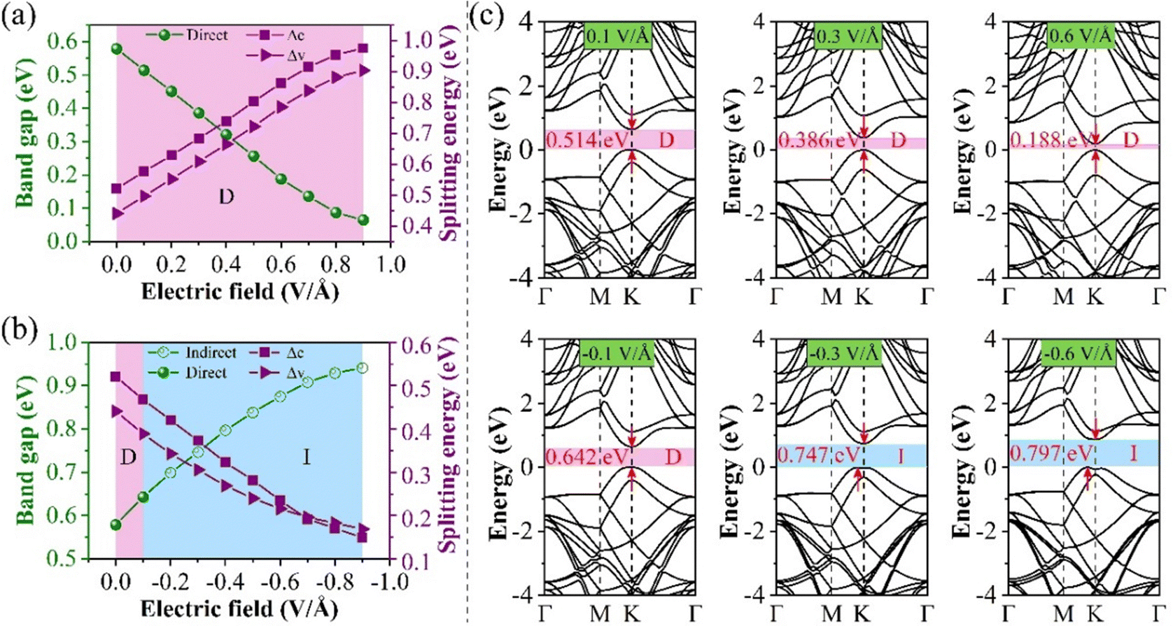 | ||
| Fig. 6 Schematic diagrams of Eg and splitting energy for 0° structure (a) positive E⊥, (b) negative E⊥, and (c) the BS at different E⊥. | ||
It can be seen from Fig. 6(a) that as the forward E⊥ strength increases, the enhanced Ein leads to a gradual decrease in its Eg, and Δc and Δv gradually increase. However, the characteristic of the direct bandgap is still maintained. When a negative E⊥ is applied, as shown in Fig. 6(b), Eg is proportional to the strength of E⊥, while Δc and Δv are inversely proportional to the strength of E⊥. When the E⊥ strength is from 0.0 to −0.1 V Å−1, it is considered a direct bandgap, but when the strength is between −0.1 and −0.9 V Å−1, the system is classified as an indirect bandgap. Fig. 6(c) shows the BS at a specific E⊥ intensity. Fig. 6(c) shows the band structure at a specific E⊥ intensity. When the system is an indirect bandgap, the VBM of the CBM is located at the K point. When the system is an indirect bandgap semiconductor, the VBM is located near the K point, while the CBM is also located at the K point. In addition, by comparing the curvature of the VBM and the CBM in Fig. 6(c), we observe that the curvature increases while the effective mass decreases with an increase in the forward E⊥, so the mobility is larger.
For the influence of E⊥ on the BS, we further calculate the electrostatic potential and the relative band edge position at field strengths of −0.3, 0.0, and 0.3 V Å−1, as shown in Fig. 7. When E⊥ is −0.3 V Å−1, since the direction of E⊥ is opposite to that of Ein, the potential barrier will be weakened and Eg will increase. The potential barrier increases, and Eg decreases. Fig. 7 illustrates this trend more graphically, showing that the system has maintained the type-II band alignment. In addition, we also demonstrated the distribution of the wave function for the CBM and the VBM (Fig. S7, ESI†). The CBM is mainly contributed by the 2p of the B atom located in the bottom BP, while the VBM is mainly contributed by the 3p of the P atom in the top BP. When an external electricity field is applied to the surface of the 2D material, the vacuum layer is used as the dielectric layer. The gradient of electrostatic potential under an external electric field indicates the strength of the external electric field, which has nothing to do with the convergence of the electrostatic potential. For details, please refer to Table S7 and Fig. S8 in the ESI.†
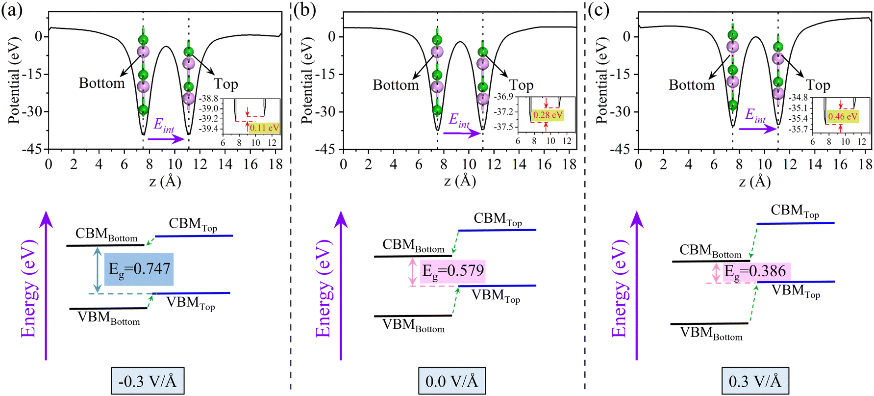 | ||
| Fig. 7 The electrostatic potential and band arrangement of the 0° is arranged under the approach of E⊥ intensity of (a) −0.3 V Å−1, (b) 0.0 V Å−1, and (c) 0.3 V Å−1, respectively. | ||
Under the action of E⊥ on the band arrangement, the possibility of exciton dissociation into an electron and a hole is very high. Therefore, the study of exciton binding energy (Eexc) is crucial for optoelectronic devices. The Eexc was calculated using formula (7), and Table 3 provides a detailed overview of the data for each parameter under the PBE method. The results show that when no E⊥ is applied, the Eexc of monolayer BP is 816.51 meV, while that of the bilayer 0° structure is 573.67 meV, indicating that bilayer BP is more likely to promote the separation of excitons. When we apply an E⊥ at –1.0 V to 1.0 V Å−1, Eexc shows a trend of initially increasing and then decreasing, which is primarily related to the change in permittivity. In addition, we found that Eexc is not the largest at 0.0 V Å−1, which may be caused by the Ein between the layers. Studies have shown that the 0° structure with a direct band gap and low Eexc under forward E⊥ has better optoelectronic performance.
 and dielectric constant (εPBE) of 0° at the PBE level. Exciton binding energies (Eexc, meV) are based on the MW method. Units of effective mass and energy are m0 and eV, respectively
| Monolayer | −0.9 V Å−1 | −0.6 V Å−1 | −0.3 V Å−1 | 0.0 V Å−1 | 0.3 V Å−1 | 0.6 V Å−1 | 0.9 V Å−1 | |
|---|---|---|---|---|---|---|---|---|

|
0.179 | 0.432 | 0.412 | 0.311 | 0.266 | 0.249 | 0.234 | 0.229 |

|
0.270 | 0.240 | 0.376 | 0.670 | 0.543 | 0.378 | 0.334 | 0.297 |

|
0.107 | 0.154 | 0.196 | 0.215 | 0.179 | 0.150 | 0.137 | 0.130 |
| ε PBE | 2.67 | 5.71 | 4.73 | 4.09 | 4.12 | 4.11 | 4.20 | 4.34 |
| E exc | 816.51 | 256.95 | 476.58 | 699.18 | 573.67 | 483.07 | 422.50 | 375.46 |
Fig. 8(a) shows the Eg values of the 13.17° structure as a function of E⊥. The results show that Eg decreases linearly with the increase of the E⊥ intensity, and Eg becomes an indirect bandgap until the E⊥ intensity exceeds 0.9 V Å−1. To study the mechanism of band change in the torsional structure, we first examine the stark splitting of the base and the CBM. Through Fig. 8(b) we observed that both Δc and Δv at 13.17° increased as positive and negative E⊥ values increased, reaching maximum values of 0.483 and 0.522 eV at −0.9 V Å−1, respectively. Then, the BS in Fig. 8(c) provides a more direct view of the changes in Δc and Δv at K point. In order to determine the band-edge contribution near the Fermi level at the K point, we analyze the distribution of the wave function at the K point (Fig. S9, ESI†). The CBM and the VBM in the forward E⊥ are contributed by the B atoms in the bottom layer and the P atoms in the top layer, respectively. The CBM and the VBM in the negative E⊥ are contributed by the B atoms in the top layer and the P atoms in the bottom layer, respectively. The 13.17° structure shows an obvious type-II band arrangement under E⊥.
 | ||
| Fig. 8 13.17° structure under different E⊥ of (a) Eg variations, (b) the splitting energy of Δc and Δc, and (c) the BS under the approach of the E⊥ intensities of 0.1, 0.3, 0.6, −0.1, −0.3, and −0.6 V Å−1. | ||
Finally, we will discuss the change in the electronic structure of the 60° structure under E⊥. First, we demonstrate that interlayer charge separation also takes place in the 60° structure when subjected to a low E⊥ intensity (Fig. S10, ESI†). From Fig. 9(a), we can see that Eg initially increases and then decreases with the change in E⊥ strength within the range of −1.3 to 1.3 V Å−1. Under positive and negative E⊥, Eg is isotropic. When the E⊥ intensity is between −1.0 and 1.0 V Å−1, the Eg changes minimally. However, when the E⊥ intensity exceeds 1.0 V Å−1, the Eg changes significantly. Therefore, the 60° structure exhibits a higher tolerance to E⊥. Since the band structure (BS) remains relatively unchanged within the range of positive and negative 1.0 V Å−1, we only present the BS for E⊥ values of 1.0, 1.1, and 1.2 V Å−1 in Fig. 9(b). It can be observed that when the E⊥ strength exceeds 1.1 V Å−1, the position of the conduction band minimum (CBM) shifts to the Γ point, which is the reason for the sudden decrease in Eg.
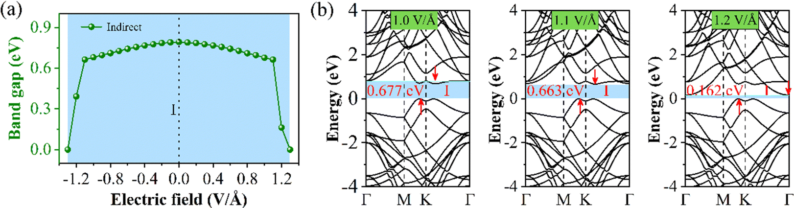 | ||
| Fig. 9 Schematic diagram of the 60° structure under E⊥, (a) Eg change, and (b) the BS under the approach of the E⊥ intensities of 1.0, 1.1, and 1.2 V Å−1. | ||
4. Conclusion
In summary, the formation energy of density functional theory calculations is used to screen the most stable stacking structure in the bilayer BP structure. Based on this structure, various torsional angle configurations are established, and the electronic properties of the torsional bilayer BP structure under E⊥ are studied. We find that the presence of a torsion angle can alter the interlayer interaction, the BS, and charge distribution. The results show that the 0° structure is different from other twisted angle structures. It exhibits a direct bandgap with intrinsic type-II energy band alignment. When E⊥ is not applied, the calculated carrier mobility is up to 104 cm2 V−1 s−1, and the photoelectric conversion efficiency is 17.3%. Then, the Eg variation under E⊥ is studied, and three types of giant Stark effects appear. It is found that due to Ein between the layers of the 0° structure when E⊥ is applied to adjust the BS, the strong Stark effect will cause the band and the valence band to split. Therefore, the Eg variation is related to the direction of E⊥, and it exhibits a linear change. By analyzing the BS and Eexc of the 0° calculated using E⊥, we conclude that the 0° structure is a promising material for photoelectric applications. However, for the structure with a torsion angle, Eg is independent of the E⊥ direction, and only depends on the E⊥ strength. Interestingly, 13.17° (21.79°, 38.21°, and 46.83°) always maintained a direct bandgap under E⊥, whereas the 60° structure consistently exhibited the characteristics of an indirect bandgap, and the other 60° had a high tolerance to E⊥. Our findings show that bilayer BP has potential applications in the fields of photovoltaics and optoelectronics, and can provide further insights into optoelectronic devices.Author contributions
Linwei Yao: conceptualization and writing – review & editing, and funding acquisition. Jiangni Yun: supervision, project administration, and funding acquisition. Peng Kang: funding acquisition. Hongyuan Zhao: methodology, investigation. Siyu Zhang: data curation, and writing – original draft. Liru Zeng: data curation and formal analysis. Zhisong Bi: writing – review & editing and visualization. Junfeng Yan: validation. Wu Zhao: validation. Zhiyong Zhang: validation.Data availability
The authors confirm that the data supporting the findings of this study are available within the article (and/or its supplementary materials).Conflicts of interest
The authors declare that they have no known competing financial interests or personal relationships that could have appeared to influence the work reported in this paper.Acknowledgements
This work was financially supported by the National Natural Science Foundation of China (51974215 and 51774223), the National Key Research and Development Program (2022YFC2904803) and Northwestern University Graduate Innovation Program (CX2023117).References
- Y. Cao, V. Fatemi and A. Demir, et al., Correlated insulator behaviour at half-filling in magic-angle graphene superlattices, Nature, 2018, 556, 80 CrossRef CAS PubMed.
- J. N. Su, J. J. Chen and M. Pan, et al., Tuning the electronic properties of HfSe2/PtSe2 heterostructure using electric field and biaxial strain, Sci. Sin. Phys., Mech. Astronomica, 2021, 51(8), 087312 CrossRef.
- H. B. Shu and X. M. Liu, Tuning electronic and optical properties of graphene/h-BN heterobilayer via surface modification, Appl. Surf. Sci., 2022, 605, 154591 CrossRef CAS.
- B. Zhou, S. J. Gong and K. Jiang, et al., A type-II GaSe/GeS heterobilayer with strain enhanced photovoltaic properties and external electric field effects, J. Mater. Chem. C, 2020, 8, 89 RSC.
- W. He, H. W. Li and H. Q. Zhou, et al., Effect of defects on the electronic structure of a PbI2/MoS2 van der Waals heterostructure: A first-principles study, Sci. China: Phys., Mech. Astronomy, 2020, 63(3), 234611 CAS.
- D. Trambly, D. Mayou and L. Magaud, Localization of Dirac Electrons in Rotated Graphene Bilayers, Nano Lett., 2010, 10(3), 804–808 CrossRef PubMed.
- G. Li, A. Luican and J. M. Lopes, et al., Observation of Van Hove singularities in twisted graphene layers, Nat. Phys., 2010, 6, 109–113 Search PubMed.
- P. Herrero and R. C. Ashoori, Massive Dirac fermions and Hofstadter butterfly in a van der Waals heterostructure, Science, 2013, 340, 1427–1430 CrossRef PubMed.
- K. S. Novoselov, E. McCann and S. V. Morozov, et al., Unconventional quantum Hall effect and Berry's phase of 2π in bilayer graphene, Nat. Phys., 2006, 2, 177–180 Search PubMed.
- S. Huang, X. Ling and L. Liang, et al., Probing the interlayer coupling of twisted bilayer MoS2 using photoluminescence spectroscopy, Nano Lett., 2014, 14(10), 5500–5508 CrossRef CAS PubMed.
- A. P. Alexander, L. B. Liang and X. F. Li, et al., Twisted MoSe2 Bilayers with Variable Local Stacking and Interlayer Coupling Revealed by Low-Frequency Raman Spectroscopy, ACS Nano, 2016, 10, 2736–2744 CrossRef PubMed.
- E. Li, J. X. Hu and X. Feng, et al., Lattice reconstruction induced multiple ultra-flat bands in twisted bilayer WSe2, Nat. Commun., 2021, 12, 5601 CrossRef CAS PubMed.
- C. Jin, E. C. Regan and A. Yan, et al., Observation of moiré excitons in WSe2/WS2 heterostructure superlattices, Nature, 2019, 567(7746), 76–80 CrossRef CAS PubMed.
- J. Kang, J. S. Li and S. Li, et al., Electronic structural Moiré pattern effects on MoS2/MoSe2 2D heterostructures, Nano Lett., 2013, 13, 5485 CrossRef CAS PubMed.
- D. Hao, Y. Xiao and C. Zi, et al., Spin-gapless and-gapped band structures of noncompensated bonding BN/Graphene bilayer, J. Phys. D: Appl. Phys., 2020, 53, 505101 CrossRef CAS.
- L. Xian, D. M. Kennes and N. Tancogne, et al., Multiat Bands and Strong Correlations in Twisted Bilayer Boron Nitride: Doping-Induced Correlated Insulator and Superconductor, Nano Lett., 2019, 19, 4934 CrossRef CAS PubMed.
- B. Zeng, M. Li and X. Zhang, et al., First-principles prediction of the electronic structure and carrier mobility in hexagonal boron phosphide sheet and nanoribbons, J. Phys. Chem. C, 2016, 120(43), 25037–25042 CrossRef CAS.
- Y. Mogulkoc, M. Modarresi and A. Mogulkoc, et al., Boron Phosphide van der Waals p-n Junction via Molecular Adsorption, Phys. Rev. Appl., 2019, 12(5), 054036 CrossRef CAS.
- H. Shu, J. Guo and X. Niu, Electronic, photocatalytic, and optical properties of two-dimensional boron pnictides, J. Mater. Sci., 2019, 54(3), 2278–2288 CrossRef CAS.
- B. Padavala, C. D. Frye and X. Wang, et al., Epitaxy of boron phosphide on aluminum nitride (0001)/sapphire substrate, Cryst. Growth Des., 2016, 16(2), 981–987 CrossRef CAS.
- M. K. Mohanta, A. Rawat and N. Jena, et al., Interfacing boron monophosphide with molybdenum disulfide for an ultrahigh performance in thermoelectrics, two-dimensional excitonic solar cells, and nanopiezotronics, ACS Appl. Mater. Interfaces, 2019, 12(2), 3114–3126 CrossRef PubMed.
- I. Joseph, K. Wan and S. Hussain, et al., Interlayer angle-dependent electronic structure and optoelectronic properties of BP-MoS2 heterostructure: a first principle study, Comput. Mater. Sci., 2021, 186, 110056 CrossRef CAS.
- M. S. Hasan Khan, M. R. Islam and M. T. Hasan, Strain-dependent electronic and optical properties of boron-phosphide and germanium-carbide hetero-bilayer: a first-principles study, AIP Adv., 2020, 10(8), 085128 CrossRef CAS.
- Y. Mogulkoc, M. Modarresi and A. Mogulkoc, et al., Electronic and optical properties of boron phosphide/blue phosphorus heterostructures, Phys. Chem. Chem. Phys., 2018, 20(17), 12053–12060 RSC.
- X. Chen, C. Tan and Q. Yang, et al., Effect of multilayer structure, stacking order and external electric field on the electrical properties of few-layer boron-phosphide, Phys. Chem. Chem. Phys., 2016, 18(24), 16229–16236 RSC.
- Y. Wang, C. Huang and D. Li, et al., Stress-and electric-field-induced band gap tuning in hexagonal boron phosphide layers, J. Phys.: Condens. Matter, 2019, 31(46), 465502 CrossRef CAS PubMed.
- J. R. Wallbank, D. Ghazaryan and A. Misra, et al., Tuning the valley and chiral quantum state of Dirac electrons in van der Waals heterostructures, Science, 2016, 353, 575–579 CrossRef CAS PubMed.
- M. Le Ster, T. Maerk and P. J. Kowalczyk, et al., Moiré patterns in van der Waals heterostructures, Phys. Rev. B: Condens. Matter Mater. Phys., 2019, 99(7), 075422 CrossRef.
- Z. Zhang, J. Li and G. Yang, et al., Interface Engineering of Band Evolution and Transport Properties of Bilayer WSe2 under Different Electric Fields, J. Phys. Chem. C, 2019, 123(32), 19812–19819 CrossRef CAS.
- C. F. Li, W. J. Zhai and Y. Q. Li, et al., Extremely flat band in antiferroelectric bilayer α-In2Se3 with large twist-angle, New J. Phys., 2021, 23(8), 083019 CrossRef CAS.
- H. Gao, J. Wang and M. Jia, et al., Two-phase interface-facilitated synthesis of graphene-like carbon nanosheets and their interfacial assembly behaviors, Chem. Phys., 2019, 516, 132–138 CrossRef CAS.
- J. P. Perdew, K. Burke and M. Ernzerhof, Generalized gradient approximation made simple, Phys. Rev. Lett., 1996, 77(18), 3865 CrossRef CAS PubMed.
- A. Tkatchenko and M. Scheffler, Accurate molecular van der Waals interactions from ground-state electron density and free-atom reference data, Phys. Rev. Lett., 2009, 102(7), 073005 CrossRef PubMed.
- J. Heyd, G. E. Scuseria and M. Ernzerhof, Hybrid functionals based on a screened Coulomb potential, J. Chem. Phys., 2003, 118(18), 8207–8215 CrossRef CAS.
- J. Bardeen and W. Shockley, Deformation potentials and mobilities in non-polar crystals, Phys. Rev., 1950, 80(1), 72 CrossRef CAS.
- J. Qiao, X. Kong and Z. X. Hu, et al., High-mobility transport anisotropy and linear dichroism in few-layer black phosphorus, Nat. Commun., 2014, 5(1), 1–7 Search PubMed.
- M. C. Scharber, D. Mühlbacher and M. Koppe, et al., Design rules for donors in bulk-heterojunction solar cells-Towards 10% energy-conversion efficiency, Adv. Mater., 2006, 18(6), 789–794 CrossRef CAS.
- J. Dai and X. C. Zeng, Bilayer phosphorene: effect of stacking order on bandgap and its potential applications in thin-film solar cells, J. Phys. Chem. Lett., 2014, 5(7), 1289–1293 CrossRef CAS PubMed.
- M. Xie, S. Zhang and B. Cai,
et al., A promising two-dimensional solar cell donor: black arsenic-phosphorus monolayer with 1.54 eV direct bandgap and mobility exceeding 14
![[thin space (1/6-em)]](https://www.rsc.org/images/entities/char_2009.gif) 000 cm2 V−1 s−1, Nano Energy, 2016, 28, 433–439 CrossRef CAS.
000 cm2 V−1 s−1, Nano Energy, 2016, 28, 433–439 CrossRef CAS. - X. Lv, W. Wei and Q. Sun, et al., Two-dimensional germanium monochalcogenides for photocatalytic water splitting with high carrier mobility, Appl. Catal., B, 2017, 217, 275–284 CrossRef CAS.
- J. M. Galicia-Hernandez, J. Guerrero-Sanchez and R. Ponce-Perez, et al., Self-energy corrected band-gap tuning induced by strain in the hexagonal boron phosphide monolayer, Comput. Mater. Sci., 2022, 203, 111144 CrossRef.
- Y. Wang, C. Huang and D. Li, et al., Tight-binding model for electronic structure of hexagonal boron phosphide monolayer and bilayer, J. Phys.: Condens. Matter, 2019, 31(28), 285501 CrossRef CAS PubMed.
- Q. Peng, K. Hu and B. Sa, et al., Unexpected elastic isotropy in a black phosphorene/TiC2 van der Waals heterostructure with flexible Li-ion battery anode applications, Nano Res., 2017, 10(9), 3136–3150 CrossRef CAS.
- Virtual NanoLab version 2015.1, QuantumWise A/S (https://www.quantumwise).
- L. Du, K. Zheng and H. Cui, et al., Novel electronic structures and enhanced optical properties of boron phosphide/blue phosphorene and F4TCNQ/blue phosphorene heterostructures: a DFT+NEGF study, Phys. Chem. Chem. Phys., 2018, 20(45), 28777–28785 RSC.
- A. Ramasubramaniam, D. Naveh and E. Towe, Tunable Band Gaps in Bilayer Transition-Metal Dichalcogenides, Phys. Rev. B: Condens. Matter Mater. Phys., 2011, 84, 205325 CrossRef.
- R. Zhang, G. Hao and X. Ye, et al., Tunable electronic properties and Schottky barrier in a graphene/WSe2 heterostructure under out-of-plane strain and an electric field, Phys. Chem. Chem. Phys., 2020, 41, 23699–23706 RSC.
- Z. Xie, F. Sun and R. Yao, et al., Tuning electronic properties of InSe/arsenene heterostructure by external electric field and uniaxial strain, Appl. Surf. Sci., 2019, 475, 839–846 CrossRef CAS.
- S. Sahoo, M. C. Sahu and S. K. Mallik, et al., Electric field-modulated charge transfer in geometrically tailored MoX2/WX2 (X = S, Se) heterostructures, J. Phys. Chem. C, 2021, 125(40), 22360–22369 CrossRef CAS.
- Y. Li, J. K. Qin and C. Y. Xu, et al., Electric field tunable interlayer relaxation process and interlayer coupling in WSe2/graphene heterostructures, Adv. Funct. Mater., 2016, 26(24), 4319–4328 CrossRef CAS.
Footnote |
| † Electronic supplementary information (ESI) available. See DOI: https://doi.org/10.1039/d3cp03591c |
| This journal is © the Owner Societies 2024 |