
Effects of gamma radiation on the electrical properties of InAs/InGaAs quantum dot-based laser structures grown on GaAs and Si substrates by molecular beam epitaxy
M. Al
Huwayz
ab,
D. A.
Jameel
 *c,
Walter M.
de Azevedo
d,
Jorlandio F.
Felix
e,
N. Al
Saqri
f,
O. M.
Lemine
g,
S. Abu
Alrub
g and
M.
Henini
b
*c,
Walter M.
de Azevedo
d,
Jorlandio F.
Felix
e,
N. Al
Saqri
f,
O. M.
Lemine
g,
S. Abu
Alrub
g and
M.
Henini
b
aDepartment of Physics, College of Sciences, Princess Nourah bint Abdulrahman University (PNU), Riyadh, 11671, Saudi Arabia
bSchool of Physics and Astronomy, University of Nottingham, Nottingham, NG7 2RD, UK
cDepartment of General Sciences, College of Basic Education, University of Zakho, Zakho, Kurdistan Region Iraq, Iraq. E-mail: dler.jameel@uoz.edu.krd
dDepartamento de Química Fundamental, Universidade Federal de Pernambuco (UFPE), 50740-560, Recife/PE, Brazil
eInstitute of Physics, NFA, University of Brasília (UnB), Brasília, DF 70910-900, Brazil
fDepartment of Physics, College of Science, Sultan Qaboos University, Box 36, Al Khoud 123, Oman
gDepartment of Physics, College of Sciences, Imam Mohammad Ibn Saud Islamic University (IMISU), Riyadh 11623, Saudi Arabia
First published on 25th November 2023
Abstract
This study investigates the impact of gamma radiation on the electrical properties of InAs/InGaAs quantum dot-based laser structures grown on both GaAs (Sample A) and Si (Sample B) substrates using molecular beam epitaxy. The research explores the electrical characteristics of the lasers before and after being exposed to gamma radiation employing current–voltage (I–V), capacitance–voltage (C–V), deep level transient spectroscopy (DLTS) and Laplace DLTS techniques. The results show that the electrical properties of the lasers change due to gamma radiation exposure, and the extent of the change depends on the substrate used for growth. The I–V results revealed that the ideality factor (n) and built-in voltage were increased in Sample A and Sample B after radiation. Nonetheless, the series resistance (Rs) at room temperature decreased in both samples after radiation. Overall, this study provides valuable insights into the effects of gamma radiation on the electrical properties of InAs/InGaAs quantum dot lasers and highlights the importance of considering substrate materials in the design of radiation-hardened electronic devices.
1 Introduction
Within the field of QD systems, the area of InAs QDs has attracted much research activity, which is due to the possibility of achieving light emission covering the optical communication wavelength bands.1–3 The study of the electrical properties of any semiconductor material is important in order to understand the possibility of using them in different electronic and optoelectronic applications. Electrical properties of PN junctions and Schottky diodes are affected by a multitude of factors. These include interface chemistry, processing methodology, the existence of native defects referred to as interface states and doping concentration of the semiconductor.4 In addition, modifying the atomic configuration and inducing other defects into the lattice has been found to take place through exposure of semiconductor materials to radiation, which consequently changes their electrical and optical properties.4,5 It is therefore important to investigate the effect of radiation on the performance of semiconductor-based devices such as Schottky diodes, solar cells, lasers, heterostructures and metal-insulator/oxide-semiconductors due to the fact that they are used in satellites. A significant number of lattice defects are produced in semiconductors as a result of radiation in space, which reduce the devices’ performance.6,7 Moreover, the study of the defects induced by radiation led to better devices used in space, which are more radiation-resistant.To investigate the effect of electron irradiation and proton hydrogenation on the electrical properties of GaAsN devices grown by chemical beam epitaxy (CBE) on the main nitrogen-related nonradiative recombination center E1, which has an activation energy of 0.33 eV below the bottom edge of the conduction band, B. Bouzazi et al.8 employed the deep level transient spectroscopy (DLTS) technique. Their study proposed that the origin of this defect is related to the compensation of the tensile strain in the film produced by the small atomic size of N atom compared to that of As. In addition, the density of E1 increased with increasing the fluency doses of electron irradiation.8
Furthermore, the effect of gamma irradiation on the electron traps present in as-grown liquid encapsulated Czochralski GaAs was described by T. Hashizume and H. Hasegawa.5 They discovered that following irradiation, the concentration of EL6 (0.35 eV) trap was reduced by a factor of 3–5, whereas the density of EL3 (0.56 eV) increased by a factor of one order of magnitude.5,9
The effect of gamma irradiation on dilute GaAsN layers with different nitrogen concentrations ranging from 0.2 to 1.2% grown on n+ GaAs substrates by molecular beam epitaxy (MBE) was investigated by N. Al Saqri et al.10 by using the DLTS and Laplace DLTS (LDLTS) techniques. According to their study, the number of traps either decreased, remained the same or new traps were created after irradiation depending on the nitrogen content.
This paper presents an experimental investigation on the effect of gamma irradiation on InAs/InGaAs QD lasers grown on GaAs and Si substrates using current–voltage (I–V), capacitance–voltage (C–V), deep level transient spectroscopy (DLTS) and Laplace DLTS measurement techniques. The experimental results showed that gamma irradiation improves the electrical properties of the devices, due to the reduction of the concentration of the defects and/or their transformation.
2 Sample details
In this work, the samples investigated are p–i–n laser diodes with InAs self-assembled quantum dots (QDs) incorporated in the i-region. The samples were fabricated using the same technique as reported in ref. 11 and 12. In summary, the InAs QD lasers are deposited on (100) n-type GaAs (Sample A: control sample) and (100) n-type Si substrates (Sample B). The Sample A consists of the following layers: a 50 nm n-GaAs buffer, a thin film of 1500 nm n-Al0.42Ga0.58As covering layer, a 108 nm undoped GaAs spacer layer, 4 × [2.5 monolayers (MLs) InAs QDs/10 nm In0.15Ga0.85As (strain reducing layer, SRL)/40 nm GaAs/10 nm In0.15Ga0.85As (SRL)], a 64 nm undoped GaAs spacer layer, a 1500 nm p-Al0.42Ga0.58As cladding layer, and a thin film of 300 nm p-GaAs. The InAs QDs were deposited at a temperature of 500 °C and a growth rate of 0.03 monolayer ML/s. Before the growth of the 6 nm In0.15Ga0.85As SRL followed by 10 nm thick GaAs layers, a short deposition interruption under As2 flux was introduced. Subsequently, the growth temperature was increased to 570 °C to deposit the remaining GaAs cap layer. The covering, contact, and spacer layers were deposited at 570 °C.The layers of Sample B, grown on n-type Si substrate, were grown utilizing the same technique and growth conditions as used for Sample A except for the buffer layer, which is designed and utilized to reduce the defects produced from the lattice mismatch between Si and GaAs substrates. Finally, the Ohmic contacts were obtained by thermal evaporation of 99.99% Au on the p+ GaAs films with the area of 2.83 × 10⁻³ cm2 for Sample A: as-grown, Sample A: irradiated and Sample B: as-grown; and area of 5.02 × 10⁻³ cm2 for Sample B: irradiated. The I–V measurements were performed utilizing a current–voltage (I–V) source-meter unit (model Keithley 236) and a closed-loop helium cryostat model CCS-450 (Janis Research Company). The capacitance–voltage (C–V) measurements were done employing an LCR meter (Agilent E4980A). Finally, the temperature-dependent DLTS and LDLTS measurements have been carried out on all the samples using a temperature controller (Lake Shore 331), capacitance meter (Boonton 7200) and pulse generator (Agilent 33220A). To investigate the impact of radiation on the InAs QD laser structures grown on n-type GaAs and Si substrates, the samples were irradiated with a gamma cell Cobalt Irradiator (dose rate of 5.143 kGys hour−1) at a high dose of 50 kGy.
3 Results and discussion
3.1 Current–voltage (I–V) measurements
In order to investigate the effect of gamma irradiation on the electrical properties of the InAs/InGaAs QD laser structures grown on GaAs (Sample A) and Si (Sample B) substrates, I–V measurements at different temperatures were performed. Fig. 1(a) and 2(a) illustrate the current–voltage (I–V) characteristics at room temperature of Sample A and Sample B, respectively, before and after irradiation. However, due to the different areas of the samples and for comparison purposes, the current density (J) versus reverse bias is plotted for both samples, as shown in Fig. 1(b) and 2(b).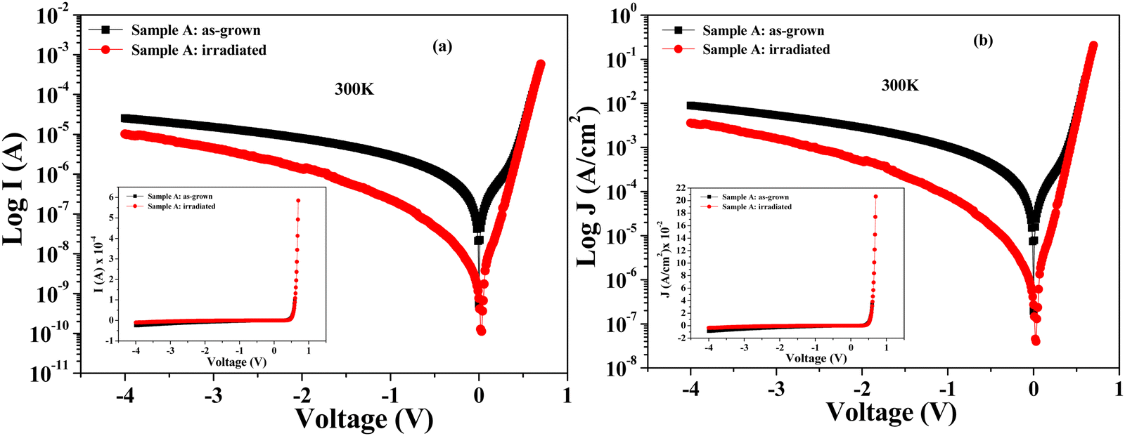 | ||
| Fig. 1 (a) Room temperature semi-log plot (I–V) characteristics of Sample A: as-grown and irradiated. (b) Semi-log plot (J–V) characteristics of Sample A: as-grown and irradiated with the same area of A = 2.83 × 10⁻³ cm2. The insets in (a) and (b) show a linear I–V plot and a linear J–V plot, respectively. | ||
 | ||
| Fig. 2 (a) Room temperature semi-log plot (I–V) characteristics for Sample B: as-grown and irradiated. (b) Room temperature semi-log plots of dark J–V characteristics for Sample B: as-grown (A = 2.83 × 10⁻³ cm2) and irradiated (A = 5.02 × 10⁻³ cm2). The insets in (a) and (b) show a linear I–V plot and a linear J–V plot, respectively. | ||
As shown in Fig. 1(b), the J–V characteristics of Sample A improved after irradiation. The reverse current of the irradiated Sample A is lower than that of the as-grown Sample A. On the other hand, since the contact areas of as-grown Sample B (effective diode area A = 2.83 × 10⁻³ cm2) and the irradiated sample (A = 5.02 × 10⁻³ cm2) are different, the current density (J) is plotted in Fig. 2 instead of current (I). As clearly seen in Fig. 2, Sample B grown on Si substrates also exhibited lower reverse currents after irradiation. However, the decrease in reverse current density after irradiation is larger for Sample A. For example, at VR = −1 V, the current density in Sample A decreased from 1.04 × 10⁻³ A to 8.04 × 10⁻⁵ A after irradiation, while at the same reverse voltage, the current density of Sample B decreased from 1.28 × 10⁻⁴ A cm−2 to 1.57 × 10⁻⁵ A cm−2. This decrease in reverse current after irradiation in both Sample A and Sample B may indicate that the density of the defects in the as-grown samples decreased and/or the number of defects changed by annihilation or generation. In addition, the deep level defects can act as generation recombination centers and most likely they will play a role in carrier recombination in the reverse current characteristics.13,14
In order to study the electrical parameters of the diodes, such as ideality factor (n), built-in potential (Vbi), and series resistance (Rs), the thermionic emission equation15 was used, which is represented by:
 | (1) |
 | (2) |
In the above equations, q is the electronic charge, V is the applied voltage, T is the absolute temperature in Kelvin, kB is the Boltzmann constant, A** is the effective Richardson's constant for a semiconductor material and A is the diode area.
The enhanced Werner's approach was used to increase the precision of the characteristic parameters (n, Vbi, and Rs) of the devices.16 The values of n, Vbi, and Rs over the temperature of 160–420 K were obtained. The J–V characteristics for all samples were analysed further to understand their properties by calculating the local ideality factor, n(V), using the following approximation equation.17,18
 | (3) |
The local ideality factors for all samples are calculated at room temperature and their values change with voltage, as shown in Fig. 3. As can be seen from Fig. 3, for each device there are two noticeable behaviours observed at low voltage (∼0.08 V) and high voltage (0.3 V) regions. In particular, at high voltages, Sample A exhibits a clear peak before and after irradiation. In addition, irradiated Sample A shows a pronounced peak at low voltages. However, for Sample B these peaks are less significant at low voltages and absent at high voltages for both as-grown and irradiated devices. This behaviour of the local ideality factor could indicate that there are different conduction mechanisms occurring in the investigated devices.17,18 Moreover, in all samples the values of the ideality factor (n) are greater than unity for voltages greater than ∼0.05 V, indicating carrier recombination mechanisms such as band-to-band radiative recombination, Shockley–Read–Hall recombination (also called trap-assisted recombination) through defects, and defect-assisted tunnelling or surface recombination.19,20 These processes could possibly explain the large ideality factors observed in these samples, which incorporate QDs in the intrinsic region and which create an additional current component that contributes to the total current of the devices. It is worth pointing out that Sample B (as-grown and irradiated) has a different trend at high voltage ranges (i.e., no peak is observed), which suggests that some mechanisms are presumably suppressed or enhanced by growing on Si substrates, and some of the mechanisms are possibly unique to the devices grown on Si.
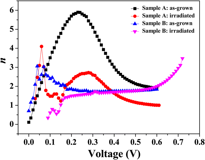 | ||
| Fig. 3 Voltage dependence of the local ideality factor for as-grown and irradiated Sample A and Sample B at 300 K. | ||
Table 1 summarises the electrical parameters of the diodes at room temperature. As-grown Sample A has a lower ideality factor (n = 1.54), a slightly lower built-in potential energy (Vbi = 0.63 eV) and a higher series resistance (Rs = ∼221 kΩ) when compared to irradiated Sample A (n = 1.86; Vbi = 0.74 eV; Rs = ∼20 × 10−3 kΩ). Likewise, as-grown Sample B has a slightly lower value of ideality factor (n = 1.70), lower built-in potential energy (Vbi = 0.63 eV) and slightly larger series resistance (Rs = ∼2.31 × 10⁻³ kΩ) when compared to irradiated Sample B (n = 1.73; Vbi = 0.67 eV; Rs = ∼3.5 × 10⁻⁴ kΩ). At room temperature, both as-grown samples have ideality factors close to unity, whereas a deviation of n from unity can indicate that the conduction mechanism can be dominated by the diffusion mechanism (thermionic emission) and other factors such as series resistance, interface states, generation-recombination mechanism.21–24
| Sample ID | n | V bi (eV) | R s (kΩ) |
|---|---|---|---|
| Sample A: as-grown | 1.54 | 0.63 | 221.58 |
| Sample A: irradiated | 1.86 | 0.74 | 20 × 10−3 |
| Sample B: as-grown | 1.70 | 0.63 | 2.31 × 10⁻³ |
| Sample B: irradiated | 1.73 | 0.67 | 3.5 × 10⁻⁴ |
Fig. 4–6 show the behaviours of built-in potential energy (Vbi), series resistance (Rs) and ideality factor (n) as a function of temperature, respectively, for Sample A and Sample B before and after irradiation. As shown in Fig. 4, the built-in potential energy increases with increasing temperature before and after radiation for Sample A. This temperature dependence of the built-in potential energy is due to the effect of potential in-homogeneities at the p–i–n interface.25 The built-in potential energy of Sample A after irradiation increased for all temperatures as compared to the as-grown sample. A similar trend was observed for irradiated Sample B for temperatures up to ∼280 K, but for temperatures >∼280 K, the Vbi values of the as-grown and irradiated Sample B were similar.
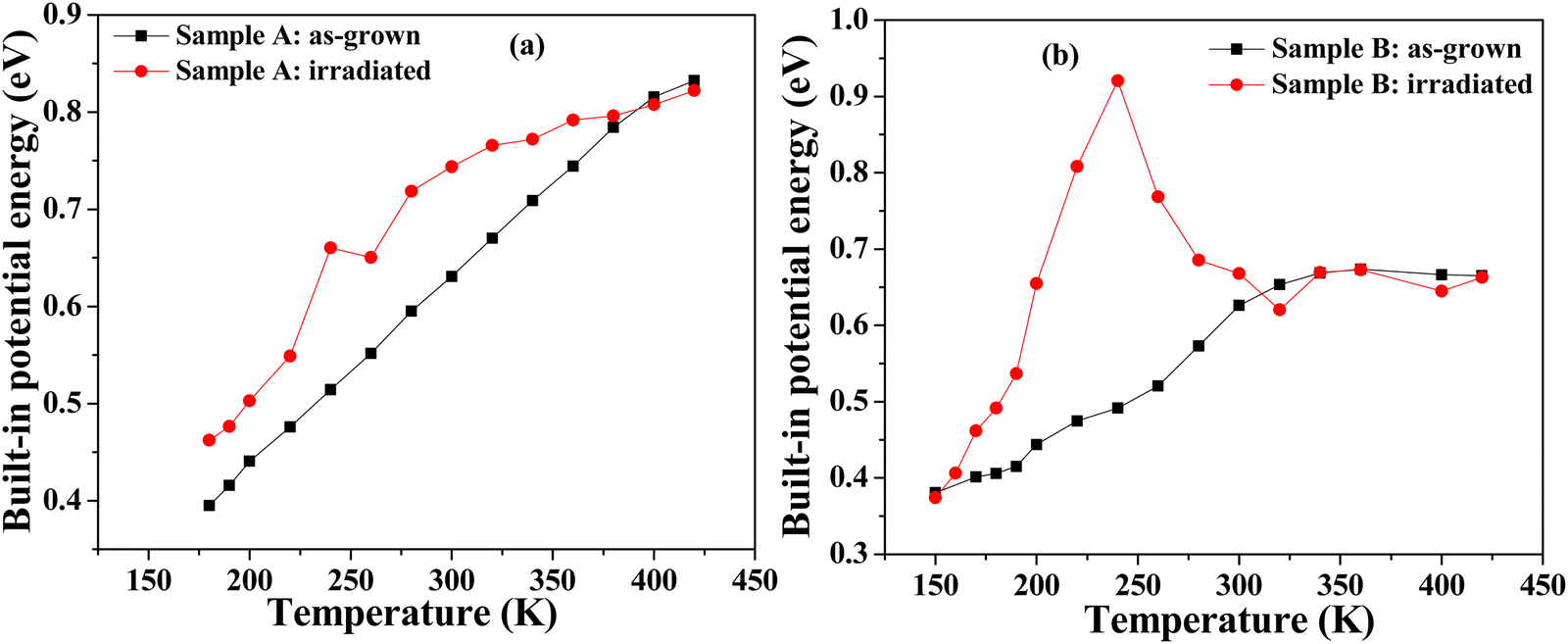 | ||
| Fig. 4 Temperature dependence of the experimental built-in potential energy of as-grown and gamma irradiated: (a) Sample A; (b) Sample B. | ||
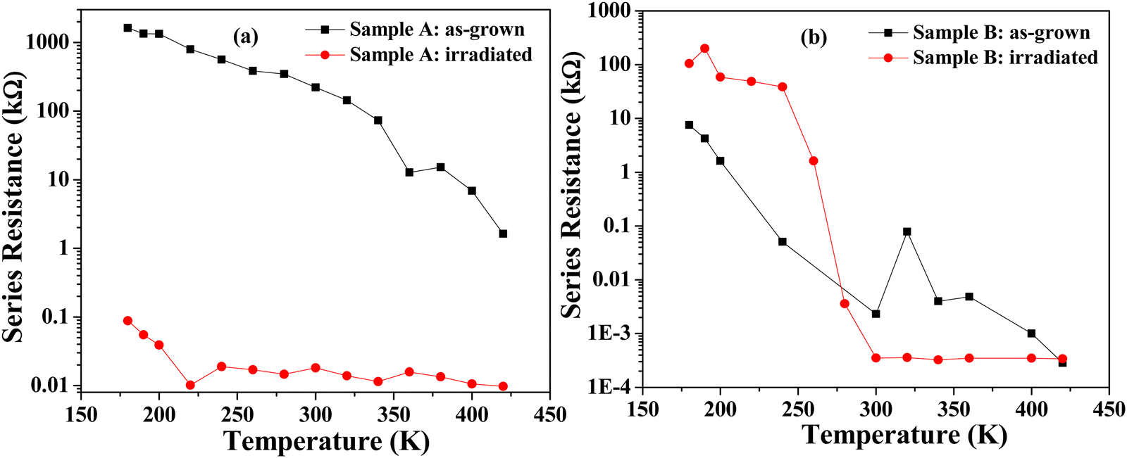 | ||
| Fig. 5 Temperature dependence of the experimental series resistance determined from I–V characteristics of as-grown and gamma irradiated: (a) Sample A; (b) Sample B. It is important to note that the as-grown sample has a smaller area than the irradiated sample. | ||
 | ||
| Fig. 6 Temperature dependence of the experimental ideality factor of as-grown and gamma irradiated: (a) Sample A; (b) Sample B. | ||
Fig. 5 shows the dependence of the series resistance as a function of temperature of Sample A and Sample B before and after irradiation. As shown in Fig. 5, this behaviour is different for both samples. The series resistance of as-grown Sample A, which decreased with increasing temperature, became very small and practically independent of temperature. However, for Sample B, the low and temperature insensitive series resistance of the as-grown structure showed a decaying behaviour with increasing temperature after irradiation. In addition, it can be seen from Fig. 5 that the resistance of Sample A and Sample B changed rapidly with temperature. These results are associated with gamma radiation which has the capability to cause an increase in temperature, thereby inducing structural alterations in the multilayer materials. In this scenario, gamma radiation may initiate a form of thermal annealing, inducing a process of activation of dopants, which in turn contributes to the improvement of the electrical properties of the devices.
The ideality factor of the irradiated samples A and B became more uniform and did not change very much for temperatures greater than ∼225 K and ∼275 K, respectively, as shown in Fig. 6. However, the ideality factors of samples A and B were smaller after irradiation for temperatures lower than 200 K and 250 K, respectively.
3.2 Capacitance–voltage (C–V) measurements
C–V measurements were recorded at room temperature utilizing a BOONTON 7200 capacitance meter to determine the free carrier concentration (Nd) of both samples. Fig. 7(a) and 8(a) illustrate the capacitance–voltage (C–V) characteristics at room temperature of Sample A and Sample B, respectively, before and after irradiation. On the other hand, due to the difference in the area of the samples, the change of capacitance per area at room temperature as a function of reverse bias of all samples is plotted as shown in Fig. 7(b) and 8(b) for comparison purposes. Fig. 7(a) and (b) show that the change of capacitance is similar for Sample A before and after irradiation. The capacitance of the as-grown and irradiated Sample B also follows a similar trend, as shown in Fig. 8(a) and (b), respectively. As clearly seen in Fig. 7 and 8 the capacitance of both Sample A and Sample B decreases after irradiation. However, the decrease in capacitance/area is more pronounced in the irradiated Sample A than in the irradiated Sample B.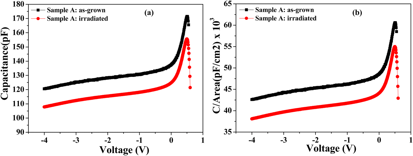 | ||
| Fig. 7 (a) Variation of capacitance C versus reverse bias V at room temperature for Sample A: as-grown and irradiated. (b) C/area–V characteristics for Sample A: as-grown (A = 2.83 × 10⁻³ cm2) and irradiated (A = 2.83 × 10⁻³ cm2). | ||
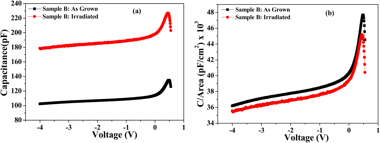 | ||
| Fig. 8 (a) Variation of capacitance C versus reverse bias V at room temperature for Sample B: as-grown and irradiated. (b) C/area–V characteristics for Sample B: as-grown (A = 2.83 × 10⁻³ cm2) and irradiated (A = 5.02 × 10⁻³ cm2). | ||
It is important to note from Fig. 7 and 8 that after irradiation, the capacitance values decreased in all samples. This decrease can be attributed to the dielectric constant change at the p–i–n interface and/or the reduction of net ionized dopant concentration due to the capture of charge carriers by defects.26–28
On the other hand, as can be noticed in Fig. 9, the plots of 1/C2versus reverse bias V for all samples at room temperature are nonlinear revealing that the junction doping profiles (concentration of carriers as a function of depletion width) are neither uniform nor linearly graded,29i.e. they are not abrupt. These results for all samples infer non-uniformity in the carrier distribution at the interface and away from the interface. These effects could cause a non-homogeneous or a spatially distributed barrier potential at the interface. As a result, the gamma radiation dose does not impact on the junction doping profiles.
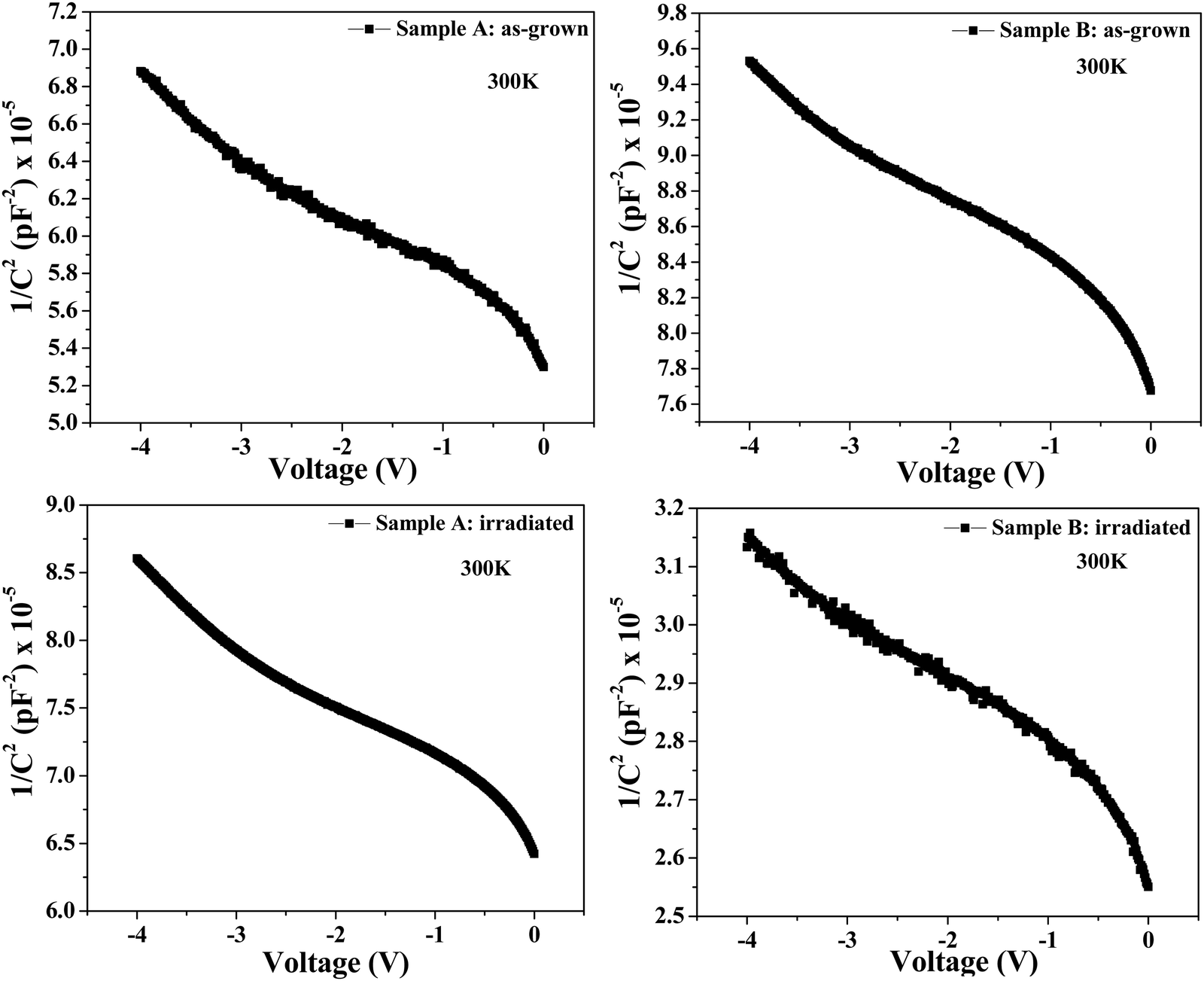 | ||
| Fig. 9 Plots of 1/C2versus V for both as-grown and irradiated samples at room temperature. The solid lines represent the best fit to the data points. | ||
3.3 DLTS and LDLTS measurements
DLTS and LDLTS measurements30,31 were performed in the temperature range of 20–440 K in both Samples A and B before and after irradiation in order to investigate the effect of gamma irradiation on deep-level defects at a filling pulse height VP = 0 V, pulse width of tP = 1 ms, rate window of 200 s−1 and reverse bias of VR = −4 V.Fig. 10(a) and (b) presents the DLTS spectra, before and after irradiation for both Sample A and Sample B with reverse bias of −4 V. It can be seen that the DLTS signal of Sample A did not change after irradiation. Whereas the DLTS signal of Sample B increased by approximately half after irradiation.
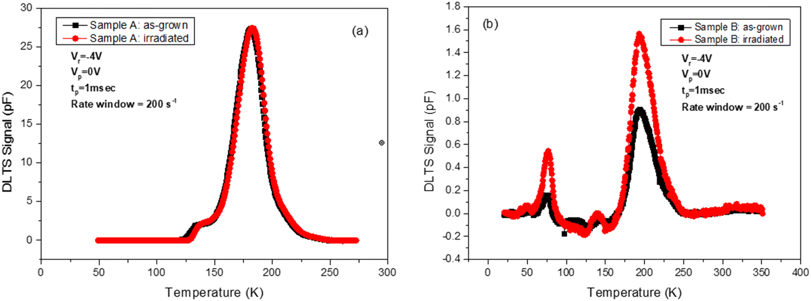 | ||
| Fig. 10 DLTS spectra of as-grown and irradiated: (a) Sample A and (b) Sample B at VR = −4 V. | ||
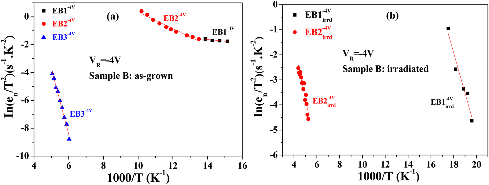
Laplace DLTS was used to resolve the broader peaks observed in conventional DLTS. Fig. 11 and 12(a) and (b) show Arrhenius plots of ln(en/T2) vs. (1000/T) for reverse bias of −4 V for Sample A and Sample B before and after radiation.
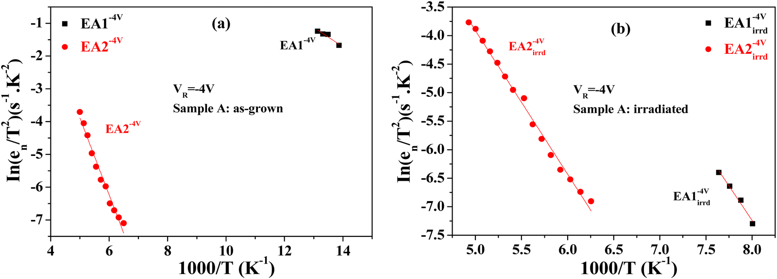 | ||
| Fig. 11 Arrhenius plots obtained from Laplace DLTS spectra with reverse biases VR = −4 V, filling pulse height VP = 0 V, and filling pulse time tP = 1 ms. For Sample A (a) as-grown and (b) after irradiation. The labelling A and E refer to Sample A (before and after irradiation) and electron traps, respectively. The solid lines represent the best fit to the data points. | ||
 | ||
| Fig. 12 Arrhenius plots obtained from Laplace DLTS spectra with reverse biases VR = −4 V, filling pulse height VP = 0 V, and filling pulse time tP = 1 ms. For Sample B (a) as-grown and (b) after irradiation. The labelling B and E refer to Sample B (before and after irradiation) and electron traps, respectively. The solid lines represent the best fit to the data points. | ||
The activation energy (ET), trap concentration (NT), and captured cross-section (σ∞) of all defects detected were extracted from these plots and the DLTS/LDLTS spectra. Tables 2 and 3 summarise these parameters.
| Sample ID | Reverse bias (V) | Trap | Activation energy (eV) | Trap concentration (cm−3) | Capture cross-section σ∞ (cm2) |
|---|---|---|---|---|---|
| Sample A as-grown | −4 | EA1−4V | 0.05 ± 0.01 | 7.58 × 10¹⁴ | 3.02 × 10⁻¹⁸ |
| EA2−4V (EL5)31 | 0.45 ± 0.08 | 2.7 × 10¹⁶ | 2.87 × 10⁻¹⁷ | ||
| Sample A irradiated | −4 | EA1Irrd−4V (EL10)32 | 0.21 ± 0.02 | 7.60 × 10¹⁵ | 8.10 × 10⁻¹⁶ |
| EA2Irrd−4V (EL10)32 | 0.22 ± 0.01 | 1.52 × 10¹⁷ | 3.23 × 10⁻¹⁷ |
| Sample ID | Reverse bias (V) | Trap | Activation energy (eV) | Trap concentration (cm−3) | Capture cross-section σ∞ (cm2) |
|---|---|---|---|---|---|
| Sample B as-grown | −4 | EB1−4V | 0.0030 ± 0.0002 | 4.96 × 10¹⁵ | 2.12 × 10⁻¹⁷ |
| EB2−4V | 0.067 ± 0.003 | 8.54 × 10¹⁵ | 1.8 × 10⁻¹⁷ | ||
| EB3−4V (EL5)31 | 0.41 ± 0.01 | 3.3 × 10¹⁵ | 3.9 × 10⁻²⁰ | ||
| Sample B irradiated | −4 | EB1Irrd−4V (EL10)32 | 0.14 ± 0.02 | 6.94 × 10¹⁴ | 2.73 × 10⁻²⁰ |
| EB2Irrd−4V (EL10)32 | 0.22 ± 0.02 | 6.58 × 10¹⁵ | 3.24 × 10⁻¹⁸ |
Tables 2 and 3 show that the number of defects is larger in the samples grown on Si substrates. It is also important to note that in general, the defects detected in both samples (A and B) after irradiation have different parameters than those observed in as-grown samples (A and B).
At VR = −4 V, the number of defects (i.e., number of trap energy levels) increased to two for both as-grown and irradiated Sample A. As-grown Sample A displayed two electron traps, namely EA1−4V (0.05 ± 0.01 eV) and EA2−4V (0.45 ± 0.08 eV). Likewise, irradiated Sample A presented two electron traps, namely EA1Irrd−4V (0.21 ± 0.02 eV) and EA2Irrd−4V (0.22 ± 0.01 eV). However, as-grown Sample B has three electron traps EB1−4V (0.0030 ± 0.0002 eV), EB2−4V (0.067 ± 0.003 eV) and EB3−4V (0.41 ± 0.01 eV), while the number of defect traps (i.e., number of trap energy levels) in irradiated Sample B decreased to two, namely EB1Irrd−4V (0.14 ± 0.02 eV) and EB2Irrd−4V (0.22 ± 0.02 eV).
In addition, at reverse bias voltage VR = −4 V, the traps EA2−4V (0.45 ± 0.08 eV) and EB3−4V (0.41 ± 0.01 eV) with similar activation energies and present in both as-grown samples (Sample A and Sample B) could also be of the same origin and attributed to EL5 (∼0.43 eV), which was assigned to complexes involving As interstitials-Ga vacancies (AsiVGa).32 After irradiation this trap was annihilated in both samples, and new deep defects were created, namely EA2Irrd−4V and EB2Irrd−4V, with similar activation energies of ∼0.22 eV. These traps could be of the same origin, and could be related to EL10 (∼0.18 eV)33 which was ascribed to an arsenic vacancy (VAs) complex defect involving an impurity.34–36
It is important to note that the shallow traps EA1−4V (0.05 eV), EB1−4V (0.0030 eV) and EB2−4V (0.067 eV) detected only in as-grown samples have not been reported previously in the literature, and therefore their origins could not be identified in this work, but these could be related to shallow impurities introduced either intentionally or unintentionally. It important to mention that no shallow defects were observed in the irradiated samples.
In summary, the gamma radiation has an effect on the electrically active defects present in as-grown InAs/InGaAs QDs lasers grown on GaAs and Si substrates. This effect led to the number of traps either decreasing, remaining the same or new traps being created after irradiation.
4 Conclusion
I–V, C–V, DLTS and Laplace DLTS were used to investigate the effect of gamma irradiation on the electrical properties of InAs/InGaAs QD lasers grown on GaAs and Si substrates by MBE. From I–V measurements, the ideality factor (n) and built-in voltage were increased in both samples after radiation. However, the series resistance (Rs) at room temperature decreased in Sample A and Sample B after radiation.In terms of the gamma radiation effect on the electrically active defects, the number of traps for Sample A was unchanged but the activation energies and trap concentrations changed after irradiation. However, gamma radiation affected the electrically active defects of Sample B, in which the number of traps decreased from three to two traps. Moreover, the DLTS and Laplace DLTS have been able to reveal a close connection between the grown-in defects and those induced by radiation.
Data access statement
Data sets generated during the current study are available from the corresponding author on reasonable request.Ethics statement
We, the authors of this paper, affirm our commitment to ethical research practices and have taken all necessary steps to ensure the credibility and validity of the results presented. This ethics statement serves as a testament to our dedication to upholding the highest ethical standards in scientific inquiry.Conflicts of interest
The authors declare that they have no known competing financial interests or personal relationships that could have appeared to influence the work reported in this paper.Acknowledgements
This work was supported and funded by the Deanship of Scientific Research at Imam Mohammad Ibn Saud Islamic University (IMSIU) (grant number IMSIU-RP23089). We thank Dr A. Salhi from Hamad Bin Khalifa University, Qatar, for providing the samples investigated in this work.References
- A. Creti, et al., Role of charge separation on two-step two photon absorption in InAs/GaAs quantum dot intermediate band solar cells, Appl. Phys. Lett., 2016, 108(6) DOI:10.1063/1.4941793.
- M. V. Maksimov, et al., High-power 1.5 μm InAs–InGaAs quantum dot lasers on GaAs substrates, Semiconductors, 2004, 38(6), 732–735, DOI:10.1134/1.1766381.
- A. Salhi, S. Alshaibani, Y. Alaskar, A. Albadri and A. Alyamani, Achieving wavelength emission beyond the C-band from Type-II InAs–GaAsSb quantum dots grown monolithically on silicon substrate, J. Alloys Compd., 2019, 771, 382–386, DOI:10.1016/j.jallcom.2018.08.276.
- I. P. Vali, et al., Gamma irradiation effects on Al/n-Si Schottky junction properties, Nucl. Instrum. Methods Phys. Res., Sect. B, 2018, 436, 191–197, DOI:10.1016/j.nimb.2018.09.035.
- T. Hashizume and H. Hasegawa, Variation of deep electron traps created by γ irradiation of GaAs, J. Appl. Phys., 1990, 68(9), 4598–4603, DOI:10.1063/1.346168.
- G. A. Umana-Membreno, J. M. Dell, G. Parish, B. D. Nener, L. Faraone and U. K. Mishra, 60Co gamma irradiation effects on n-GaN Schottky diodes, IEEE Trans. Electron Devices, 2003, 50(12), 2326–2334, DOI:10.1109/TED.2003.820122.
- J. F. Felix, et al., Effect of gamma radiation on the electrical properties of Polyaniline/silicon carbide heterojunctions, Radiat. Meas., 2014, 71, 402–406, DOI:10.1016/j.radmeas.2014.05.014.
- B. Bouzazi, N. Kojima, Y. Ohshita and M. Yamaguchi, Effect of electron and proton irradiation on recombination centers in GaAsN grown by chemical beam epitaxy, Curr. Appl. Phys., 2013, 13(7), 1269–1274, DOI:10.1016/j.cap.2013.03.017.
- T. Richter, G. Kühnel, W. Siegel and J. R. Niklas, Activation energies of the EL6 trap and of the 0.15 eV donor and their correlation in GaAs, Semicond. Sci. Technol., 2000, 15(11), 1039–1044, DOI:10.1088/0268-1242/15/11/305.
- N. Al Saqri, et al., Investigation of the effects of gamma radiation on the electrical properties of dilute GaAs1−xNx layers grown by Molecular Beam Epitaxy, Curr. Appl. Phys., 2015, 15(10), 1230–1237, DOI:10.1016/j.cap.2015.07.010.
- M. Al Huwayz, et al., Effects of substrate material on the electrical properties of self-assembled InAs quantum dots-based laser structures, Appl. Phys. A: Mater. Sci. Process., 2023, 129(6), 405, DOI:10.1007/s00339-023-06626-w.
- M. Al Huwayz, et al., Optical properties of self-assembled InAs quantum dots based P–I–N structures grown on GaAs and Si substrates by Molecular Beam Epitaxy, J. Lumin., 2022, 251 DOI:10.1016/j.jlumin.2022.119155.
- S. Alhassan, et al., Investigation of the effect of substrate orientation on the structural, electrical and optical properties of n-type GaAs1−xBix layers grown by Molecular Beam Epitaxy, J. Alloys Compd., 2021, 885 DOI:10.1016/j.jallcom.2021.161019.
- Ö. Güllü, F. Demir, F. E. Cimilli and M. Biber, γ-Irradiation-induced changes at the electrical characteristics of Sn/p-Si Schottky contacts, Vacuum, 2008, 82(8), 789–793, DOI:10.1016/j.vacuum.2007.11.006.
- S. F. Chung, T. C. Wen and A. Gopalan, Influence of dopant size on the junction properties of polyaniline, Mater. Sci. Eng., B, 2005, 116(2), 125–130, DOI:10.1016/j.mseb.2004.09.023.
- J. H. Werner, Schottky barrier and pn-junction I/V plots – Small signal evaluation, Appl. Phys. A Solids Surfaces, 1988, 47(3), 291–300, DOI:10.1007/BF00615935.
- T. Gu, M. A. El-Emawy, K. Yang, A. Stintz and L. F. Lester, Resistance to edge recombination in GaAs-based dots-in-a-well solar cells, Appl. Phys. Lett., 2009, 95(26) DOI:10.1063/1.3277149.
- H. F. Lu, L. Fu, G. Jolley, H. H. Tan, S. R. Tatavarti and C. Jagadish, Temperature dependence of dark current properties of InGaAs/GaAs quantum dot solar cells, Appl. Phys. Lett., 2011, 98(18) DOI:10.1063/1.3586251.
- A. B. M. H. Islam, D. S. Shim and J. I. Shim, Enhanced radiative recombination rate by local potential fluctuation in InGaN/AlGaN near-ultraviolet light-emitting diodes, Appl. Sci., 2019, 9(5) DOI:10.3390/app9050871.
- N. I. Bochkareva, et al., Defect-related tunneling mechanism of efficiency droop in III-nitride light-emitting diodes, Appl. Phys. Lett., 2010, 96(13) DOI:10.1063/1.3367897.
- B. Şahin, H. Çetin and E. Ayyildiz, The effect of series resistance on capacitance-voltage characteristics of Schottky barrier diodes, Solid State Commun., 2005, 135(8), 490–495, DOI:10.1016/j.ssc.2005.05.050.
- M. A. Ebeoǧlu, F. Temurtas and Z. Z. Öztürk, Ag/n-GaAs Schottky mis diodes with surface insulating layers prepared using (NH4)2S solutions without water, Solid. State. Electron., 1998, 42(1), 23–27 CrossRef.
- R. T. Tung, J. P. Sullivan and F. Schrey, On the inhomogeneity of Schottky barriers, Mater. Sci. Eng., B, 1992, 14(3), 266–280, DOI:10.1016/0921-5107(92)90309-W.
- E. Rhoderick and R. Williams, Metal-Semiconductor Contacts. 1988, Clarendon, Clarendon Press, Oxford, 2nd edn, 1988 Search PubMed.
- A. Chitnis, et al., High-quality p-n junctions with quaternary AllnGaN/InGaN quantum wells, Appl. Phys. Lett., 2000, 77(23), 3800–3802, DOI:10.1063/1.1331084.
- P. Zukowski, J. Partyka and P. Wegierek, Effect of ion implantation and annealing on the dielectric properties of silicon, Phys. Status Solidi Appl. Res., 1997, 159(2), 509–515, DOI:10.1002/1521-396X(199702)159:2
![[double bond splayed right]](https://www.rsc.org/images/entities/char_e00a.gif) 509::AID-PSSA5093.0.CO;2-K.
509::AID-PSSA5093.0.CO;2-K. - M. Nishiguchi, et al., Radiation tolerant GaAs MESFET with a highly-doped thin active layer grown by OMVPE, IEEE Trans. Nucl. Sci., 1990, 37(6), 2071–2075, DOI:10.1109/23.101231.
- Ş. Karataş, A. Türüt and Ş. Altindal, Effects of 60Co γ-ray irradiation on the electrical characteristics of Au/n-GaAs (MS) structures, Nucl. Instrum. Methods Phys. Res., Sect. A, 2005, 555(1–2), 260–265, DOI:10.1016/j.nima.2005.09.017.
- D. A. Jameel, Electrical performance of organic/inorganic hybrid solar cell devices based on n-type GaAs substrate orientations and a conjugated polymer (PANI), Appl. Phys. A: Mater. Sci. Process., 2021, 127(7) DOI:10.1007/s00339-021-04718-z.
- D. V. Lang, Deep-level transient spectroscopy: a new method to characterize traps in semiconductors, J. Appl. Phys., 1974, 45, 3023 CrossRef CAS.
- L. Dobaczewski, A. R. Peaker and K. Bonde Nielsen, Laplace-transform deep-level spectroscopy: the technique and its applications to the study of point defects in semiconductors, J. Appl. Phys., 2004, 96(9), 4689–4728, DOI:10.1063/1.1794897.
- K. Yokota, H. Kuchii, K. Nakamura, M. Sakaguchi, H. Takano and Y. Ando, EL2, EL3, and EL6 defects in GaAs highly implanted with sulfur, J. Appl. Phys., 2000, 88(9), 5017, DOI:10.1063/1.1315331.
- N. P. Khuchua, L. V. Khvedelidze, M. G. Tigishvili, N. B. Gorev, E. N. Privalov and I. F. Kodzhespirova, Deep-level effects in GaAs microelectronics: a review, Russ. Microelectron, 2003, 32(5), 257–274, DOI:10.1023/A:1025528416032.
- R. Yakimova, T. Paskova and C. Hardalov, Behavior of an EL5-like defect in metalorganic vapor-phase epitaxial GaAs:Sb, J. Appl. Phys., 1993, 74(10), 6170–6173, DOI:10.1063/1.355184.
- D. V. Lang, A. Y. Cho, A. C. Gossard, M. Ilegems and W. Wiegmann, Study of electron traps in n-GaAs grown by molecular beam epitaxy, J. Appl. Phys., 1976, 47(6), 2558–2564, DOI:10.1063/1.322974.
- P. Blood and J. J. Harris, Deep states in GaAs grown by molecular beam epitaxy, J. Appl. Phys., 1984, 56(4), 993–1007, DOI:10.1063/1.334040.
| This journal is © the Owner Societies 2024 |