
First principles predictions of structural, electronic and topological properties of two-dimensional Janus Ti2N2XI (X = Br, Cl) structures†
Shiladitya
Karmakar
 ,
Soumendu
Datta
and
Tanusri
Saha-Dasgupta
*
,
Soumendu
Datta
and
Tanusri
Saha-Dasgupta
*
S.N. Bose National Centre for Basic Sciences. JD Block, Sector III, Salt Lake, Kolkata 700106, India. E-mail: tanusri@bose.res.in
First published on 18th March 2024
Abstract
Motivated by the report of the giant Rashba effect in ternary layered compounds BiTeX, we consider two Janus structured compounds Ti2N2XI (X = Br, Cl) of the same ternary family exhibiting a 1![[thin space (1/6-em)]](https://www.rsc.org/images/entities/char_2009.gif) :1:1 stoichiometric ratio. Broken inversion symmetry in the Janus structure, together with its unique electronic structure exhibiting anti-crossing states formed between Ti-d states and strong spin–orbit coupled I-p states, generates large Rashba cofficients of 2–3 eV Å for these compounds, classifying them as strong Rashba compounds. The anti-crossing features of the first-principles calculated electronic structure also result in non-trivial topology, combining two quantum phenomena – Rashba effect and non-trivial topology – in the same materials. This makes Janus TiNI compounds candidate materials for two-dimensional composite quantum materials. The situation becomes further promising by the fact that the properties are found to exhibit extreme sensitivity and tunability upon application of uniaxial strain.
:1:1 stoichiometric ratio. Broken inversion symmetry in the Janus structure, together with its unique electronic structure exhibiting anti-crossing states formed between Ti-d states and strong spin–orbit coupled I-p states, generates large Rashba cofficients of 2–3 eV Å for these compounds, classifying them as strong Rashba compounds. The anti-crossing features of the first-principles calculated electronic structure also result in non-trivial topology, combining two quantum phenomena – Rashba effect and non-trivial topology – in the same materials. This makes Janus TiNI compounds candidate materials for two-dimensional composite quantum materials. The situation becomes further promising by the fact that the properties are found to exhibit extreme sensitivity and tunability upon application of uniaxial strain.
1 Introduction
Since the discovery of the monolayer structure of carbon atoms by exfoliating graphite into graphene with unprecedented properties,1,2 there has been a surge of activity in the field of two-dimensional (2D) materials, opening up a 2-dimensional era.3–7 Following this exciting discovery, several elemental and binary 2D materials have been synthesized and studied, e.g. graphane,8 h-BN,9 transition metal dichalcogenides,10 silicene,11,12 and phosphorene.13 It becomes necessary to expand the 2D materials library further by adding new compositional combinations and layer arrangement types.Following this, in recent times, ternary layered materials have generated considerable interest. While they can be of different stoichiometric ratios, there are a large class of layered materials exhibiting a stoichiometric ratio of 1:1:1, containing one metallic element and two nonmetallic elements, one of which is a halogen. They are layered structures, where each monolayer consists of a fluorite-type [M2O2] or [M2N2] or [M2C2] layer (here M is the metallic element) sandwiched between two layers of halogen. In particular, the Group IVB transition metal nitride halides (MNX; M = Ti, Zr, Hf; X = Cl, Br, I) have attracted considerable attention with reports on their properties like superconductivity,14–16 hydrogen storage capability17,18 and novel electronic properties.19 The Group IVB transition metals are non-toxic and the MNX materials are, therefore, environment friendly. The non-metallic elements are the p-block elements, and the structure–property relationship of these materials is expected to be influenced by the inherent orbital-hybridization of the partially filled valence p-orbitals of the non-metallic elements with the less than half-filled valence d-orbital of the transition metal element M.
Given that each layer of 111-type compounds is stacked together by the van der Waals (vdW) force, they can be mechanically exfoliated into atomic-thick 2D nanosheets. For example, bulk titanium nitride halides have an orthorhombic α phase under the ambient conditions, belonging to a class of layered materials with the space group Pmmn.20 Due to their layered structures and the weak van der Waals interaction between the consecutive slabs through the non-metallic halogen atoms, much efforts have been devoted to studying the properties of the TiNX 2D structures by the ab initio density functional theory (DFT) calculations. All these studies indicate that exfoliation of a single slab of TiNX from the bulk TiNX crystal structure is energetically possible,21–25 making the situation hopeful. These first-principles studies further indicate that upon increasing the atomic number of the halogen species, moving from F to Cl to Br to I, the systems show a wide band gap semiconducting to moderate band-gap semiconducting to semi-metallic behaviour due to tuning of Ti–X hybridization.26 The semi-metallic behaviour of TiNI with strong spin–orbit coupled I-dominated states close to the Fermi level opens up the possibility of realizing TiNI-based 2D topological materials. Indeed, first-principles calculations performed by Wang et al. predicted that the TiNI 2D band structure would possess a topologically non-trivial bandgap at the Dirac point.22 The hybrid functional based calculation27 predicted the non-trivial topological character of strained 2D TiNI structures.
In this context, it is crucial to determine whether further functionalities can be introduced in this exciting class of materials. Designing Janus monolayers by breaking the inversion and/or out-of-plane mirror symmetry in a pristine monolayer is a promising approach for tailoring and improving the properties of the pristine monolayer. In this context, it is worth mentioning that BiTeX compounds (X = halogen), belonging to the same family of 1:1:1 ternary 2D materials, are reported to exhibit a giant Rashba effect28,29 due to the broken mirror and inversion symmetries in the alternate stacking of Bi, Te and X layers within the monolayer structure of BiTeX.30,31 Following a similar idea, in the present study, we focus on two Janus monolayers, Ti2N2ClI and Ti2N2BrI, derived from the pristine TiNI monolayer by replacing one of the two terminating I-layers with a Cl layer for the Janus Ti2N2ClI monolayer and with a Br-layer for the Janus Ti2N2BrI monolayer.32 Since the successful synthesis of the Janus MoSSe monolayer through a controlled change of the stoichiometric ratio by the chemical vapour deposition (CVD) growth technique,33,34 many stable Janus monolayers have been predicted theoretically.35–37 Due to the broken out-of-plane inversion symmetry and the presence of an intrinsic finite out-of-plane dipole moment arising from the electronegativity difference between the two different terminating halogen species, Janus Ti2N2XI (X = Cl, Br) monolayers are expected to provide a finite Rashba effect.38 This along with non-trivial topological properties of parent TiNI, if retained in the Janus structure, can open up the possibility of realizing yet another example of a two-dimensional composite quantum material, which exhibits more than one apparently distinct quantum phenomenon fulfilling the common requirement of different symmetries in a single material.
Using first principles DFT calculations, we analyze the structural, electronic, and topological properties. Our calculations reveal a large Rashba coefficient of 2.67 eV Å for the Janus Ti2N2BrI monolayer and 3.28 eV Å for the Janus Ti2N2ClI monolayer, arising from band anticrossing, classifying these 2D compounds as strong Rashba compounds. The two-dimensionality of the proposed systems with giant values of Rashba coefficients makes them ideally suited for the fabrication of spintronic devices. Interestingly, while the inclusion of Cl or Br helps to break the symmetries, the Cl/Br dominated states appear far from the Fermi level, keeping the band structure close to the Fermi level nearly intact, thereby retaining the non-trivial topological properties. This makes the Janus Ti2N2ClI and Ti2N2BrI monolayers examples of unique 2D composite quantum materials connecting topological non-triviality and strong Rashba effects. Furthermore, the application of uniaxial strain is found to affect the above properties in a non-trivial manner. Due to distinctly different bonding properties along the crystallographic a and b directions, the uniaxial strain applied along the a or b-axis is found to result in highly anisotropic changes. The strain property phase diagram is found to consist of a number of distinct diverse phases – (i) large Rashba, topologically non-trivial, semi-metallic; (ii) large Rashba, topologically trivial, semi-metallic; and (iii) small Rashba, topologically trivial, semi-conducting. Thus strain-induced phase transitions are observed between topologically non-trivial to trivial, large to small Rashba, and semi-metallic to semi-conducting, making TiNI-based 2D Janus structures a rich platform for future investigation.
2 Computational details
DFT based first-principles electronic structure calculations were carried out using plane-wave basis and projector augmented-wave (PAW) pseudopotentials in combination with Perdew–Burke–Ernzerhof (PBE) generalized gradient approximation (GGA) as the exchange–correlation functional39 as implemented in the plane-wave based Vienna ab initio simulation package (VASP).40In the valence electronic configuration within the PAW basis set, we considered 4 electrons for Ti (3d34s1), 5 electrons for N (2s22p3) and 7 electrons for halogen X (ns2np5) atoms with n = 3, 4 and 5 respectively for Cl, Br and I. The cutoff energy of the plane-wave basis was chosen to be 600 eV, which was found to be sufficient to achieve convergence in self-consistent field (SCF) calculations. Dispersion correction at the D3 level41 was included in all calculations. To minimize artificial interaction between a 2D material and its images along the out-of-plane direction within the periodic set-up of calculation, a converged vacuum space of ∼24 Å was used.
Relaxation of Ti2N2XI structures was carried out with respect to internal atomic coordinates and unit cell volume using a convergence threshold of 10−5 eV for total energy and 10−3 eV Å−1 for the maximum force component on an atom. A converged Monkhorst–Pack42k-mesh of 9 × 9 × 1 was used for SCF calculations with a tight energy convergence threshold of 10−8 eV. The relativistic spin–orbit coupling (SOC) was included. The electronic band structure along high symmetry points of the first Brillouin zone (BZ) of the optimized orthorhombic lattice was computed within both PBE + D3 and PBE + D3 + SOC formalisms. The dynamical and thermal stabilities of the constructed structures were checked using phonon spectra and molecular dynamics simulation, the details of which are given in the ESI† Sections SI and SII.
To calculate the topological properties, maximally localized Wannier functions (MLWFs) for each structure were computed to derive a tight-binding model from the first principle calculations using the WANNIER90 code.43 The initial guess orbital basis sets were 3d orbitals on Ti, 5p orbitals on I, and 4p(3p) orbitals on Br(Cl). To find out the topological nature, we calculated the Z2 topological invariant following the procedure by Soluyanov et al.,44 which uses the notion of Wannier charge centers (WCCs). The Wannier functions (WF) associated with any unit cell are given by
 | (1) |
3 Results and discussion
3.1 Optimized structures of the monolayers
Fig. 1(A) shows the structure of the pristine TiNI monolayer, obtained by extracting a monolayer from the α-phase crystal structure of the bulk TiNI, followed by structural optimization. The structure contains two Ti atoms, two N atoms and two I atoms in the orthorhombic unit cell. The primary feature of the structure is buckled double M–N layers of width d, sandwiched between top and bottom halogen layers, resulting in a single-layer TiNI structure of total width W. Within the orthorhombic crystal structure of the α-form, Ti atoms are six-coordinated by four nitrogen atoms and two terminating halogen atoms forming an octahedron around each Ti atom, as shown in the right panel of Fig. 1(A). While the Ti–N–Ti bond-angle is nearly 180° along the crystallographic a direction, the Ti–N–Ti bond-angle along the crystallographic b direction and the Ti–I–Ti bond-angle deviate strongly from 180° resulting in a highly distorted octahedral environment around the Ti atom. The optimized structure of the pristine TiNI monolayer belonging to the centrosymmetric space group Pmmn contains 8 symmetry operations – identity (E), inversion centre (i) at the (0,1/4) site, three 2-fold rotation axes (C2) along [1,0,0], [0,1,0], [0,0,1] directions (the former two C2 axes are combined with screw components along [1/2,0,0] and [0,1/2,0] directions respectively), two mirror planes perpendicular to [1,0,0] and [0,1,0], one glide-plane perpendicular to [0,0,1] with the glide component along [1/2,1/2,0]. The right panel illustration of Fig. 1(A) shows the inversion centers and the C2 rotation axes. | ||
| Fig. 1 Crystal structures of a pristine TiNI monolayer (A) and a Janus Ti2N2XI monolayer (B). Titanium (Ti), nitrogen (N), iodine (I), and X atoms are shown as sky-blue, grey, magenta, and red-coloured balls, respectively. Terminating I, X-layers, and middle Ti-layers are indicated by magenta, red, and sky blue coloured atomic planes. The width of the monolayers, W, and the inner (Ti2N2)2+ laminar width, d, are marked by double-headed arrows. The distorted octahedral environment of Ti atoms along with the two-fold rotation axes (C2) and inversion centres in the pristine TiNI monolayer and Janus Ti2N2XI monolayer is also shown. Creation of a Janus structure breaks the inversion symmetry and generates two inequivalent Ti atoms, shown as light blue and red shaded octahedra in the Janus structure. | ||
Two Janus Ti2N2XI (X = Cl/Br) monolayers are constructured by considering the optimized structure of the pristine TiNI monolayer and replacing its top iodine layer by the atoms of the X halogen species, followed by further optimization of the resultant structures. The construction of the Janus structure, as shown in Fig. 1(B), makes the chemical environment of the two Ti atoms in the unit cell different, with two inequivalent Ti sites. Similar to the structure of the pristine TiNI monolayer, both Ti atoms are at distorted octahedral coordination in the structure of the Janus monolayer, but along the c-axis, one Ti-octahedron is coordinated by the I atom while the other by the X (= Br, Cl) atom, shown with different colours in the right panel of Fig. 1(B). Upon creation of a Janus Ti2N2XI monolayer, the symmetry gets lowered compared to the pristine TiNI monolayer. In particular, the structure loses the inversion centres as shown in Fig. 1 along with two screw axes, and therefore also the glide plane. This results in a noncentrosymmetric space group Pmm2 (no. 25) containing 4 symmetry operations for each Janus monolayer.
While the dynamic and thermal stability of the pristine TiNI monolayer has been ascertained before, we repeated the same exercise for the two Janus structures. In particular, to confirm the dynamical stability of these structures, vibrational phonon calculations were performed as presented in the ESI† Section S1 for all three monolayers. We found that TiNI and Ti2N2XI (X = Cl, Br) monolayers have similar phonon dispersions, with the absence of imaginary phonon modes over the entire Brillouin zone, signalling their dynamical stability. Additionally, ab initio MD simulation at 300 K for 20 ps confirms the thermal stability of the structures (cf. Section S2 of the ESI†). We also calculated the formation energy46 defined through Eform = Eslab − [2 × (μTi + μN) + μI + μX]. Eslab is the total energy corresponding to the optimized structure of the respective monolayer and μ's are the chemical potentials. The formation energy is estimated with respect to the chemical potential of bulk hexagonal Ti (μTi = −7.75 eV per atom) and the nitrogen molecule (μN = 1/2μN2 = −8.31 eV per atom) and dimer molecule of the associated halogen species (i.e. μCl = 1/2μCl2 = −1.78 eV per atom; μBr = 1/2μBr2 = −1.52 eV per atom; μI = 1/2μI2 = −1.48 eV per atom). Our estimated values of the formation energies for the studied monolayers are given in Table 1. It is seen that the creation of Janus structures makes the formation energy further negative, indicating the energetic stability. Furthermore, the bonding strength of these monolayers can be estimated from the elastic constants, Cij, which are listed in Table 1. The calculated Cij values are found to be larger compared to those found for other 2D materials like MoS2,47 GeS,48 and GaS,49 indicating that TiNI and the derived Janus structures possess a stronger bonding than the majority of other 2D materials. The proposed Janus structures are thus mechanically, dynamically and thermally stable.
| System | a (Å) | b (Å) | d (Å) | W (Å) | E form (eV f.u.−1) | Elastic constants (N m−1) | |||
|---|---|---|---|---|---|---|---|---|---|
| C 11 | C 12 | C 22 | C 66 | ||||||
| Ti2N2ClI | 3.963 | 3.368 | 1.442 | 5.522 | −4.474 | 184.90 | 40.75 | 153.32 | 69.76 |
| Ti2N2BrI | 3.938 | 3.426 | 1.410 | 5.639 | −4.335 | 179.27 | 32.73 | 147.83 | 66.58 |
| TiNI | 3.941 | 3.515 | 1.400 | 5.812 | −4.062 | 159.26 | 44.06 | 154.41 | 64.51 |
The fully optimized lattice parameters, a and b, of the Janus Ti2N2XI monolayers along with the width of the Ti2N2 lamina and the total width of the monolayer are listed in Table 1, in comparison to that of the pristine TiNI monolayer. We find that while the lattice parameter a exhibits minimal variation upon Janusian construction, the lattice parameter b shows a marked deviation from that of pristine TiNI, highlighting the inherent anisotropy of these 2D materials. The same is reflected in the difference between C11 and C22. A compression in the total width W is noticed due to a change in the atomic size of halogens, while the width d of the [Ti2N2]2+ lamina slightly increases for the Janus monolayers compared to that of the pristine TiNI monolayer caused by the potential difference between two inequivalent Ti atoms in the two layers.
3.2 Electronic properties and Rashba effect
The evolution of orbital-projected electronic band structure between the pristine TiNI and the two Janus structures Ti2N2XI (X = Br/Cl) is shown in Fig. 2. The upper panels (Fig. 2A–C) show the results obtained in the absence of the SOC effect, while the bottom panels (Fig. 2D–F) show the results obtained by turning on the SOC effect. The basic nature of the band structure remains nearly the same between the pristine and Janus structures, with the states above the Fermi level (EF) being dominated by Ti-3d character and the states below EF being dominated by N-p and halogen-p characters. Bands with the projection of Br-4p and Cl-3p orbitals appear at −1.5 eV and −2 eV below the EF respectively, thereby unaltering the basic band structure close to EF, which is dominated by Ti-3d and I-5p character. The introduction of Cl/Br in the structure, however, causes subtle changes in the band structure, as discussed in the following. The atom projected density of states is also given in the ESI† Section S3 to visualize the contribution from important orbitals of the constituent atomic species.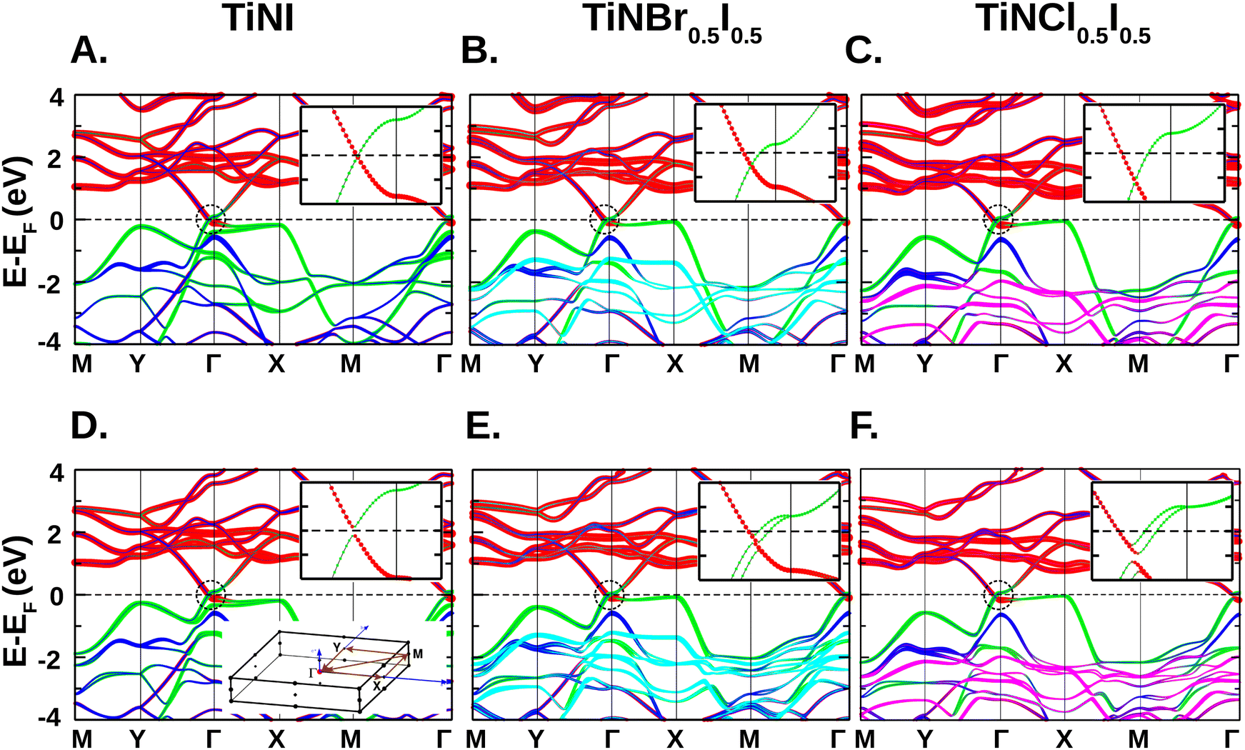 | ||
| Fig. 2 Band structure of TiNI and Janus Ti2N2XI (X = Br, Cl; the chemical formula in the figure represents one formula unit of the corresponding Janus structure) monolayers plotted along the high symmetry path M(0.5, 0.5, 0)–Y(0, 0.5, 0)–Γ–X(0.5, 0, 0)–(0.5, 0.5, 0)–Γ of the BZ (cf. bottom inset of D). The zero of the energy is set at the Fermi level. The energy bands are projected onto Ti-3d (red), N-2p (blue), I-5p (green), Br-4p (cyan) and Cl-3p (magenta) orbital characters. The top (A)–(C) and bottom (D)–(F) panels show the band structure obtained in the absence and in the presence of SOC, respectively. The insets in each panel show the orbital characters of the bands zoomed around the Fermi level highlighted by a black, dotted circle. | ||
In the absence of the SOC effect, we find from Fig. 2 that the pristine TiNI monolayer shows a semi-metallic nature as the valence band (VB) and conduction band (CB) touches at EF forming a linearly dispersing Dirac crossing along the Y–Γ k-path. The linearly touching bands are found to be formed by the intersection of Ti-3d and I-5p states, as seen in the zoomed plot in the inset of Fig. 2A. The VB top along the Γ–X k-path becomes almost flat, which is mainly contributed by the non-bonding I-5p orbitals. Upon formation of the Janus structures, the position of the Dirac crossing shifts below EF as seen in the insets of Fig. 2B and C. Thus introduction of Cl/Br in the structure results in partial occupancy of the conduction band, forming electron pockets. The electronegativity difference between the constituting halogen species in the Janus structures allows more charge transfer in comparison to that of the pristine TiNI structure. As a result, bands dominated by Ti-3d orbitals around EF get pulled downshifting the Dirac point 30 meV and 62 meV below the EF for the Janus Ti2N2BrI and Ti2N2ClI monolayers, respectively.
Upon application of the SOC effect, a small gap of 42 meV opens up, transforming the semimetallic TiNI monolayer into a narrow gap semiconductor with a direct band gap (cf. inset in Fig. 2D). Observations made for the pristine TiNI monolayer are consistent with the results of the previous literature.22,25 For the Janus Ti2N2XI monolayers, the band structures reveal the splitting of the Kramers degeneracy of the non-magnetic bands into two branches around the Dirac point due to the broken inversion symmetry. The spin degeneracy is lifted except for the Dirac point of two branches. The splitting becomes more prominent around the region dominated by I-5p orbitals due to the strong SOC effect of iodine as shown in the insets of Fig. 2E and F. We notice that the orbital character changes drastically from Ti-3d to I-5p orbitals at the Dirac point (kD) as the k-vector changes from k ≤ kD to k ≥ kD in the partially filled CB. A similar trend is observed for the next fully occupied VB as well while the k-vector changes from k ≥ kD to k ≤ kD. This signals the band anti-crossings of Rashba split Dirac bands located between the Y and Γ k-path. This leads to two consequences: (a) band inversion and (b) gap opening at the Dirac point between Rashba split bands of the Janus structures. While the former hints at non-trivial topological properties, the latter indicates a sizable Rashba parameter. Along with band anti-crossing, we also identify band-crossing between the Kramer pairs at the Γ point around which the orbital character is essentially the same (I-5p) unlike band-anticrossing. Fig. 3 shows the band-anticrossing and band-crossing points in the representative band structure of the Janus Ti2N2BrI monolayer. The effect of Coulomb interaction through PBE + D3 + U and PBE + D3 + U + SOC calculations has been checked. The primary features of the band structure including the semimetallic nature are found to remain intact as found in the previous literature.27
 | ||
| Fig. 3 Band structure of the Janus Ti2N2BrI monolayer, exhibiting band anti-crossing (encircled in blue) and band crossing (encircled in magenta). The parameters, ΔER and ΔkR, governing the Rashba parameter at the band anti-crossing and band crossing are shown in the side image. | ||
The Rashba parameter, αR, quantifying the Rashba spin splitting within the nearly free electron approximation is defined as  , where ΔER represents the energy difference between the extrema of the split bands, while ΔkR represents the distance between the same points in momentum space. First, we compute the αR due to band-anticrossing taking two Kramer pairs around the Dirac point, one representing the partially occupied CB where we consider the Rashba splitting in the I-5p orbital dominated region while the other representing the fully occupied VB where we consider the Ti-3d orbital dominated region. From the enlarged view of the encircled areas, we find that ΔER and ΔkR calculated for two Kramer pairs around the Dirac point do not vary much. ΔER and ΔkR calculated for one pair turn out to be 0.0637 eV and 0.0458 Å−1 and for the other pair 0.0651 eV and 0.0509 Å−1. Hence αR due to band-anticrossing is reported by taking an average of the αR values due to the corresponding two Kramer pairs. However, we note that the ΔER shows an order of magnitude increase in the band-anticrossing in comparison to the band-crossing case (ΔER = 0.0014 eV). Two Kramer pairs at the Dirac point exhibit significant bowing of their split branches with small momentum offset for the band-anticrossing case, whereas the Kramer pair at the Γ point exhibits weakly dispersive branches. This leads to αR (∼2.67 eV Å) for band-anticrossing an order of magnitude larger than the αR (∼0.46 eV Å) for band-crossing of the Janus Ti2N2BrI monolayer. Similarly, the αR of Janus Ti2N2ClI turns out to be 3.28 eV Å for the band-anticrossing and 0.42 eV Å for the band-crossing. The Rashba scale defined by Acosta et al.50 distinguishes the compounds with αR above the range 1.6 eV Å or so as strong Rashba compounds and compounds with αR below that range as weak Rashba compounds. Moreover, the appearance of energy band anti-crossing has been proposed to be the hallmark of strong Rashba compounds. Following that, αR computed for the band-anticrossing case makes the Janus Ti2N2XI, with X = Br, Cl monolayer to fall under the category of strong Rashba compound.
3.3 Topological properties
The band inversion observed upon inclusion of the SOC effect for the pristine TiNI monolayer hints at the non-trivial topology of the linearly dispersing bands. Indeed, previous calculation of topological invariant of Z2 for the pristine TiNI monolayer reported a non-trivial value of 1.22,25 It is to be noted that semimetallic Janus Ti2N2XI monolayers with X = Br and Cl also show band inversion just below the EF near the Γ point although Kramers degeneracy got lifted due to broken inversion symmetry. This strongly suggests non-trivial topological aspects of these Janus monolayer structures too.To understand the topological nature of the band-structure of the Janus structures, we computed the Z2 topological invariant, by employing the method proposed by Soluyanov et al.,44 which uses the notion of WCC. As described in the computational details section, WCC is the expectation value of the position operator in the state corresponding to the Wannier functions of the unit cell. The evolution of the WCCs of the maximally localized Wannier functions, along the time-reversal invariant plane kz = 0, is used to characterize the topological nature. A Kramers pair is topologically non-trivial if the corresponding WCC curves at k = 0 and k = π belong to a different branch. However, following the WCC is not so easy since they have been calculated only at discrete k points. Soluyanov and Vanderbilt44 instead came up with the suggestion to follow the maximum interspace between the WCCs instead of the curves themselves. The Z2 invariant can then be determined via the discontinuities of the maximum interspace function ζ(k) between k = 0 and k = π. Hence, Z2 is given by the number of discontinuities of ζ(k) in [0, π] modulo 2. If ζ(k) intersects the WCCs an odd number of times, it can be classified as topologically non-trivial and if it crosses the WCCs an even number of times, including zero crossings, the material is trivial.
Fig. 4 shows the evolution of the WCCs along the ky direction at kz = 0 plane plotted for TiNI as well as Janus Ti2N2XI (X = Br, Cl) monolayers. For TiNI, Wannier bands are occupied up to the EF, and 12 occupied wannier bands are considered resulting in a total of 12 WCCs for each band. We notice that the ζ(k) function (blue line) drawn parallel to ky axis intersects WCCs (red line) an odd number of times not only for centrosymmetric TiNI monolayers but for the Janus monolayers as well. This corresponds to a Z2 invariant of 1 for all cases. The TiNI monolayer turned out to be a 2D topological insulator making our calculation consistent with the previous literature.22,25 Moreover, our calculation suggests that such a non-trivial nature persists even in the semimetallic Janus structures as well if the topology between the fully occupied VB and partially occupied CB is considered in the calculation.
 | ||
| Fig. 4 The WCCs tracked along the kz = 0 plane for the pristine TiNI (A), Janus Ti2N2BrI (B) and Janus Ti2N2ClI (C) monolayers. The blue solid line indicates the maximum interspace function, ζ(k), which intersects the WCCs (red dotted) even/odd number of times in the case of topologically trivial/non-trivial materials. | ||
3.4 Strain effects
As extensively discussed in the literature, the properties of the 2D monolayer can be greatly influenced by strain engineering.51 In particular, the effect of uniaxial strain on the parent TiNI monolayer has been investigated in the previous literature.22 The effect of uniaxial strain is found to be highly anisotropic, as already expected from the anisotropic nature of elastic constants and lattice parameter variation under Janus construction. The band inversion was found to be robust to stretching along the a-direction and compression along the b-direction but was found to be gradually diminished for compression along the a-direction and stretching along the b-direction.Similarly, we consider the effect of in-plane uniaxial strain εi, (i = a, b). This is expected to tune simultaneously the Rashba, topological, and electronic properties in general. εi is defined as the difference between unstrained and strained lattice parameters, εi = (i − i0)/i0 × 100%, where i0 and i are the unstrained and strained lattice parameters, respectively. The uniaxial strain along lattice vector a- and b-directions is denoted by the symbols εa and εb respectively. We note that as the Janus structures are in the orthorhombic space group (a ≠ b), crystal symmetry remains unaltered upon application of uniaxial strain. The electronic band structures in the presence of SOC effect for each Janus monolayer as a function of uniaxial strain along both a and b directions (−6% ≤ εi ≤ 6%) are calculated and analyzed, which allow us to study the variation of Rashba splitting and topological nature with uniaxial strain.
The variation in the electronic band structure of Janus monolayers with uniaxial strain is found to be similar to that of the parent TiNI monolayer. We find that the band-anticrossing tends to diminish for compression along the a-direction and stretching along the b-direction. As a result, Rashba split bands around the Dirac point tend to lose their mixed orbital character and show quadratic dispersion around the EF. For the partially occupied Kramer pair, the contribution from the I-5p orbital tends to decrease around the Dirac point, and the corresponding region gets pushed up towards the EF gradually reducing the size of the electron pocket. Under the same conditions, the contribution from the Ti-3d orbital in the fully occupied Kramer pair tends to decrease around the Dirac point and the corresponding region gets pulled down. At certain critical values of εa and εb, semimetallic Janus monolayers convert into a direct gap semiconductor with CB and VB extrema contributed mainly by Ti-3d and I-5p orbitals respectively. Semimetal to semiconductor transition occurs at εa = −3% and εb = +3% for the Janus Ti2N2BrI monolayer, whereas for the Janus Ti2N2ClI monolayer, it takes place at εa = −5% but remain semimetallic up to εb = +6%. Band-anticrossing turns out to be robust to stretching along the a-direction and compression along the b-direction. The Janus monolayers retained the semimetallic character as εa is increased and εb is decreased up to +6% and −6% respectively. These outcomes have direct consequences in the Rashba parameter αR value and the corresponding topological nature.
Fig. 5 shows the variation of αR as a function of εa and εb for Janus Ti2N2BrI (Fig. 5A and B) and Ti2N2ClI (Fig. 5C and D) monolayers. Electronic band structures zoomed around the Dirac point corresponding to the semimetallic and the semiconducting Janus monolayers are shown in the insets of different panels of Fig. 5. αR values corresponding to semimetallic structures are calculated for band-anticrossing of Rashba split pairs and the same for semiconducting structures are calculated for band-crossing of the Rashba split VB. Clearly, αR shows a non-monotonic variation with εa and εb. Moreover, the variation of αR with εa and εb follows two distinct patterns observed for both Janus monolayers, which are directly related to the appearance of band-anticrossing. We notice that the αR decreases for compression along the a-direction and stretching along the b-direction. On the other hand, αR increases for compression along the b-direction, whereas it becomes saturated for stretching along the a-direction. Clearly, αR shows an order of magnitude decrease as the Janus monolayers tend to show semimetallic to semiconducting nature as band-anticrossing vanishes for the latter case. For the Janus Ti2N2BrI monolayer, αR decreases from 2.67 to 0.19 and 0.23 eV Å as εa and εb become −5% and +4% respectively. Similarly, αR decreases from 3.28 to 0.27 and 0.30 eV Å as εa and εb change to −5% and +5% respectively for the Janus Ti2N2ClI monolayer. On the other hand, αR values of Janus Ti2N2BrI and Ti2N2ClI can increase up to 3.93 and 4.15 eV Å as εb changes to −6% and −5% respectively.
 | ||
| Fig. 5 Effect of uniaxial strain along the a-axis (A) and (C) and b-axis (B) and (D) on the electronic, topological, and Rashba properties of Ti2N2BrI (A) and (B) and Ti2N2ClI (C) and (D) monolayers. Plotted is the variation of αR as a function of εa or εb, distinguishing between large and small αR phases. The calculation of topological properties of the electronic structure associated with each data point also reveals distinct phases with topologically non-trivial semi-metallic (marked as solid symbols) band structure with a linearly dispersing anti-crossing point (cf. inset) and topologically trivial semiconducting band structure (marked as open symbols) with parabolic dispersion (cf. inset). This leads to three distinct phases in the strain-property phase diagram, phase I (shaded in light yellow) – small αR and trivial topology, phase II (shaded in cyan) – large αR and non-trivial topology, and phase III (shaded in green) – large αR and trivial topology. | ||
The Z2 invariants of the strained Janus monolayers are determined to evaluate their topological nature. Non-trivial to trivial topological transition occurs for compression along the a-direction and stretching along the b-direction as the Janus monolayers tend to show semimetallic to semiconducting character. The critical strain for the Janus Ti2N2BrI monolayer is εa = −2% and εb = +2%, while for Janus Ti2N2ClI, εa = −4% and εb = +4%. The phase space shaded by the cyan color in each panel marks the region with Z2 = 1 in εa and εb domains, indicating the non-trivial nature of the strained Janus monolayers. Interestingly, non-trivial topology is found to be robust for compression along the b-direction and stretching along the a-direction for the Janus Ti2N2BrI and Ti2N2ClI respectively.
Analysis of the Rashba parameter and topological properties of the strained Janus monolayers reveals that three distinct phases emerge upon varying εa and εb within a range [−6%, +6%]. These phases are characterized as follows: phase I - small αR and trivial topology, phase II - large αR and non-trivial topology, and phase III - large αR and trivial topology as indicated by light yellow, cyan, and green color shaded regions. Different αR regions are decided according to the Rashba scale50 indicated by the black dashed line in each panel of Fig. 5. αR ≥ 1.6 eV Å is considered as large αR and otherwise taken as small αR. We notice that phase II spans over most of the region in both εa and εb space, which is crucial for application purposes. For the Janus Ti2N2BrI monolayer, the region lies in the limits −2% ≤ εa ≤ +4% and −6% ≤ εb ≤ +2% and for the Janus Ti2N2ClI monolayer, the corresponding limit is −4% ≤ εa ≤ +6% and −6% ≤ εb ≤ +4%. The phase II is found to be more pronounced in the Janus Ti2N2ClI than the Janus Ti2N2BrI monolayer. Strained structures that reside in the phase II region have semimetallic character. The gradual decrease in αR for compression along the a-direction and stretching along the b-direction leads to phase I. In phase I, strained structures can be semimetals and semiconductors. The transition from phase II to phase I occurs while band-anticrossing around the Dirac point diminishes and bands near EF show quadratic dispersion instead of linear dispersion as evident from the zoomed-in bandstructure around the Γ point within the narrow energy window shown in the insets of each panel of Fig. 5. We note that the stretching along the b-direction can lead to the other phase III for Janus Ti2N2BrI, whereas it does not appear for the Janus Ti2N2ClI within our studied range of ε. We have also checked the influence of biaxial strain. However, as opposed to the uniaxial strain, the effect of biaxial strain was not found to be spectacular, due to the complementary effect of strain along the a- and b-axes. In particular, a reasonable value of biaxial strain failed to open the gap and failed to affect the Rashba splitting significantly.
4 Summary and discussion
In summary, considering two Janus structures created from the pristine TiNI monolayer by replacing a layer of I by Cl and Br, we show that the presence of strong SOC effect at the I site coupled with broken inversion symmetry of the structures drives the constructed 2D systems with strong Rashba compounds, adding the Janus Group IVB transition metal nitride halides to the same list as BiTeX compounds. The delicate anti-crossings with linear dispersion formed between Ti-d and I-p states are responsible for the large Rashba effect. The same anti-crossing results in the non-trivial topology of the bands, thereby deomonstrating the promise of the Janus Ti2N2XI (X = Br, Cl) structures as two-dimensional composite quantum materials exhibiting two quantum phenomena of Rashba properties together with non-trivial topology. Application of uniaxial strain is found to be highly anisotropic and found to tune both Rasbha and topological properties, driving large to small Rashba, non-trivial to trivial topology and semi-metallic to semi-conducting electronic structures, demonstrating the extreme sensitivity and tunability of the properties.Finally, it is worth mentioning that along with the sensitivity to uniaxial strain, both the computed Rashba and topological properties also show sensitivity to the approximation used for the exchange–correlation functional. The results presented above are based on first-principles calculations carried out within the framework of PBE exchange–correlation. A recent hybrid calculation (HSE06) study27 in which a portion of the exact nonlocal Hartree–Fock exchange is mixed with the complementary DFT in local (LDA) or semilocal (GGA) approximated exchange showed semi-conducting rather than semi-metallic character of the TiNI monolayer, along with trivial topology. Consideration of uniaxial strain treated within the hybrid functional, however, was found to drive TiNI semi-metallic and topologically non-trivial,27 implying the interplay and sensitivity of computed properties to strain and exchange–correlation. It is to be noted that the application of hybrid functionals, originally designed for improving large gapped systems, to semi-metallic systems is also not beyond doubt. As discussed in the literature52 although hybrid functionals have been unbiasedly applied to the study of various materials and, in some cases, improved or similar results compared with the LDA or GGA functionals have been obtained,53–55 for near metallic systems they have to be used with caution. In particular, for metallic properties that are sensitive to the electronic structure near the Fermi energy, as in the present case, hybrid functionals may give rise to significantly worse results compared with the LDA or GGA, in terms of inaccurate results of vanishing or greatly suppressed density of states at the Fermi level and false predictions of lattice instability for systems with a strong electron-phonon coupling. Furthermore, the results of HSE06 are found to depend strongly on the parameters of the theory, namely the mixing parameter and the parameter controlling the short-rangeness of the interaction, and depending on the application may differ from the default values, which are ideally chosen to describe large-gap semiconductors.
Keeping the above discussion in mind, the conclusions drawn in the present study are expected to be qualitatively correct, while the exact location of phase boundaries drawn in Fig. 5 may depend on details of the exchange–correlation approximation used in the calculation. The electronic structure calculated within HSE06 of the two strained Janus structures, shown in Section S4 of the ESI,† demonstrates this. This makes the experimental investigation furthermore necessary to shed light on this interesting class of compounds, which appear to be a potential platform for developing competing phases.
Data availability
The data that support the findings of this study are available from the corresponding author upon reasonable request.Author contributions
T. S.-D. conceived the idea and supervised the project. S. K. and S. D. carried out the calculations and analysis of the results. The manuscript was prepated by S. K. and S. D. under the guidance of T. S.-D.Conflicts of interest
The authors declare no conflict of interest.Acknowledgements
S. K. and T. S.-D. acknowledge the Technical Research Centre funded by DST, India for computational support in this work. T. S.-D. acknowledges the J. C. Bose National Fellowship (grant no. JCB/2020/000004) for funding.References
- K. S. Novoselov, D. Jiang, F. Schedin, T. J. Booth, V. V. Khotkevich, S. V. Morozov and A. K. Geim, Two-dimensional atomic crystals, Proc. Natl. Acad. Sci. U. S. A., 2007, 102, 10451 CrossRef PubMed.
- K. Novoselov, A. Geim and S. Morozov, et al., Two-dimensional gas of massless Dirac fermions in graphene, Nature, 2005, 438, 197–200 CrossRef CAS PubMed; A. Geim and K. Novoselov, The rise of graphene, Nat. Mater., 2007, 6, 183–191 CrossRef PubMed.
- J. Peng, Z. J. Chen, B. Ding and H. M. Cheng, Recent Advances for the Synthesis and Applications of 2-Dimensional Ternary Layered Materials, Research, 2023, 6, 0040 CrossRef CAS PubMed.
- J. Chen, C. Wang, H. Li, X. Xu, J. Yang, Z. Huo, L. Wang, W. Zhang, X. Xiao and Y. Ma, Recent Advances in Surface Modifications of Elemental Two-Dimensional Materials: Structures, Properties, and Applications, Molecules, 2022, 28(1), 200 CrossRef PubMed.
- G. Chakraborty, I. H. Park, R. Medishetty and J. J. Vittal, Two-Dimensional Metal-Organic Framework Materials: Synthesis, Structures, Properties and Applications, Chem. Rev., 2021, 121(7), 3751–3891 CrossRef CAS PubMed.
- S. Zhang, S. Guo, Z. Chen, Y. Wang, H. Gao, J. Gomez-Herrero, P. Ares, F. Zamora, Z. Zhu and H. Zeng, Chem. Soc. Rev., 2018, 47, 982–1021 RSC.
- Q. H. Wang, K. Kalantar-Zadeh, A. Kis, J. N. Coleman and M. S. Strano, Electronics and optoelectronics of two-dimensional transition metal dichalcogenides, Nat. Nanotechnol., 2012, 7(11), 699–712 CrossRef CAS PubMed.
- D. C. Elias, R. R. Nair, T. M. Mohiuddin, S. V. Morozov, P. Blake, M. P. Halsall, A. C. Ferrari, D. W. Boukhvalov, M. I. Katsnelson, A. K. Geim and K. S. Novoselov, Control of graphene's properties by reversible hydrogenation: evidence for graphane, Science, 2009, 323(5914), 610–613 CrossRef CAS PubMed.
- L. Song, L. Ci, H. Lu, P. B. Sorokin, C. Jin, J. Ni and P. M. Ajayan, Large scale growth and characterization of atomic hexagonal boron nitride layers, Nano Lett., 2010, 10, 3209–3215 CrossRef CAS PubMed; I. Jo, M. T. Pettes, J. Kim, K. Watanabe, T. Taniguchi, Z. Yao and L. Shi, Thermal conductivity and phonon transport in suspended few-layer hexagonal boron nitride, Nano Lett., 2013, 13, 550–554 CrossRef PubMed; W. Auwärter, Hexagonal boron nitride monolayers on metal supports: Versatile templates for atoms, molecules and nanostructures, Surf. Sci. Rep., 2019, 74(1), 1–9 CrossRef.
- J. H. Han, M. Kwak, Y. Kim and J. Cheon, Recent Advances in the Solution-Based Preparation of Two-Dimensional Layered Transition Metal Chalcogenide Nanostructures, Chem. Rev., 2018, 118(13), 6151–6188 CrossRef CAS PubMed.
- M. Ezawa, Valley-polarized metals and quantum anomalous Hall effect in silicene, Phys. Rev. Lett., 2012, 109(5), 055502 CrossRef PubMed.
- L. Tao, E. Cinquanta and D. Chiappe, et al., Silicene field-effect transistors operating at room temperature, Nat. Nanotechnol., 2015, 10, 227–231 CrossRef CAS PubMed.
- F. Xia, H. Wang and Y. Jia, Rediscovering black phosphorus as an anisotropic layered material for optoelectronics and electronics, Nat. Commun., 2014, 5, 1–6 Search PubMed; L. Kou, C. Chen and S. C. Smith, Phosphorene: fabrication, properties, and applications, J. Phys. Chem. Lett., 2015, 6, 2794–2805 CrossRef CAS PubMed.
- A. M. Fogg, V. M. Green and D. O'Hare, Superconducting Metallocene Intercalation Compounds of β-ZrNCl, Chem. Mater., 1999, 11(2), 216–217 CrossRef CAS.
- A. Sugimoto, K. Shohara, T. Ekino, Z. Zheng and S. Yamanaka, Nanoscale electronic structure of the layered nitride superconductors α-Kx TiNCl and β-HfNCly observed by scanning tunneling microscopy and spectroscopy, Phys. Rev. B: Condens. Matter Mater. Phys., 2012, 85, 144517 CrossRef.
- S. Yamanaka, Intercalation and superconductivity in ternary layer structured metal nitride halides (MNX: M = Ti, Zr, Hf; X = Cl, Br, I), J. Mater. Chem., 2010, 20, 2922–2933 RSC.
- M. Ohashi, H. Nakano and M. Hattori, Hydrogen uptake by layer structured β-ZrNCl, Solid State Ionics, 1989, 32–33, 97–103 CrossRef.
- S. Samoto, K. Iizawa, T. Kato, M. Yamada, S. Yamanaka, K. Ohoyama, M. Ohashi, Y. Yamaguchi and T. Kajitani, Hydrogen in β-ZrNCl, J. Phys. Chem. Solids, 1999, 60, 1511–1513 CrossRef.
- X. Liu, X. An, B. Xu, Q. Xia, G. Lu, G. Yu, J. Zhang, S. Ma, Y. Wang, J. Li, H. Dong and L. Yi, Ab initio prediction of thermoelectric properties of monolayer ZrNCl and HfNCl, J. Solid State Chem., 2020, 290, 121500 CrossRef CAS; P. M. Woodward and T. Vogt, Electronic Band Structure Calculations of the MNX (M = Zr, Ti; X = Cl, Br, I) System and Its Superconducting Member, Li-Doped β-ZrNCl, J. Solid State Chem., 1998, 138(2), 207–219 CrossRef.
- S. Yamanaka, K. Itoh, H. Fukuoka and M. Yasukawa, High-Pressure Systhesis of the Polymorph of Layer Structured Compounds MNX (M = Zr, Hf; X = Cl, Br, I), Inorg. Chem., 2000, 39(4), 806–809 CrossRef CAS PubMed.
- J. Liu, X.-B. Li, D. Wang, H. Liu, P. Peng and L.-M. Liu, Single-layer Group-IVB nitride halides as promising photocatalysts, J. Mater. Chem. A, 2014, 2, 6755 RSC.
- A. Wang, Z. Wang and M. Zhao, Band inversion and topological aspects in a TiNI monolayer, Phys. Chem. Chem. Phys., 2016, 18, 22154 RSC.
- Y. Liang, Y. Dai, Y. Ma, L. Ju, W. Wei and B. Huang, Novel titanium nitride halide TiNX (X = F, Cl, Br) monolayers: potential materials for highly efficient excitonic solar cells, J. Mater. Chem. A, 2018, 6, 2073–2080 RSC.
- W. Cong and G. Gao, Titanium nitride halides monolayers: promising 2D anistropic thermoelectric materials, J. Phys.: Condens. Matter, 2020, 32, 205503 CrossRef PubMed.
- W. Lei, R. Hu, S. Han, H. Yuan, W. Jiao and H. Liu, The TiNI monolayer: a two-dimensional system with promising ferroelastic, topological, and thermoelectric properties, Phys. Chem. Chem. Phys., 2022, 24, 28134 RSC.
- M. M. Hossain and S. H. Naqib, Structural, elastic, electronic, and optical properties of layered TiNX (X = F, Cl, Br, I) compounds: a density functional theorey study, Mol. Phys., 2020, 118(3), e1609706 CrossRef.
- S. Yalameha, Z. Nourbakhsh, M. S. Bahramy and D. Vashaee, New insights into band inversion and topological phase of TiNI monolayer, Phys. Chem. Chem. Phys., 2023, 25, 12182–12191 RSC.
- Y. A. Bychkov and E. Rashba, Properties of a 2D electron gas with lifted spectral degeneracy, Pis'ma Zh. Eksp. Teor. Fiz., 1984, 39, 66–69 CAS.
- A. Manchon, H. Koo and J. Nitta, et al., New perspectives for Rashba spin-orbit coupling, Nat. Mater., 2015, 14, 871–882 CrossRef CAS PubMed.
- K. Ishizaka, M. S. Bahramy, H. Murakawa, M. Sakano, T. Shimojima, T. Sonobe, K. Koizumi, S. Shin, H. Miyahara and A. Kimura, et al., Giant Rashba-type spin splitting in bulk BiTeI, Nat. Mater., 2011, 10(7), 521–526 CrossRef CAS PubMed.
- C. J. Butler, H. H. Yang, J. Y. Hong, S. H. Hsu, R. Sankar, C. I. Lu, H. Y. Lu, K. H. O. Yang, H. W. Shiu and C. H. Chen, et al., Mapping polarization induced surface band bending on the Rashba semiconductor BiTeI, Nat. Commun., 2014, 5(1), 4066 CrossRef CAS PubMed.
- The chemical formula of the pristine titanium nitride iodide monolayer is denoted as TiNI due to the stoichiometric ratio of 1:1:1 for the three constituent atomic species. Following that convention the chemical formulas of the Janus structures in one formula unit are TiNCl0.5I0.5 and TiNBr0.5I0.5. However, since the considered Janus structures are ordered structures, it may be more appropriate to represent them as Ti2N2ClI and Ti2N2BrI. While we have consistently used the convention of Ti2N2ClI and Ti2N2BrI, in some of the figure legends the one formula unit is used.
- A.-Y. Lu, H. Zhu, J. Xiao, C.-P. Chuu, Y. Han, M.-H. Chiu, C.-C. Cheng, C.-W. Yang, K.-H. Wei, Y. Yang, Y. Wang, D. Sokaras, N. Dennis, P. Yang, D. A. Muller, M.-Y. Chou, X. Zhang and L.-J. Li, Janus monolayers of transition metal dichalcogenides, Nat. Nanotechnol., 2017, 12, 744–749 CrossRef CAS PubMed.
- J. Zhang, S. Jia, I. Kholmanov, L. Dong, D. Er, W. Chen, H. Guo, Z. Jin, V. B. Shenov, L. Shi and J. Lou, Janus Monolayer Transition-Metal Dichalcogenides, ACS Nano, 2017, 11, 8192 CrossRef CAS PubMed.
- A. C. Riis-Jensen, T. Deilmann, T. Olsen and K. S. Thygesen, Classifying the Electronic and Optical Properties of Janus Monolayers, ACS Nano, 2019, 13, 13354–13364 CrossRef CAS PubMed.
- J. Jiang and W. Mi, Two-dimensional magnetic Janus monolayers and their van der Waals heterostructures: a review on recent progess, Mater. Horiz., 2023, 10, 788–807 RSC.
- L. Zhang, Z. Yang, T. Gong, R. Pan, H. Wang, Z. Guo, H. Zhang and X. Fu, Recent advances in emerging Janus two-dimensional materials: from fundamental physics to device applications, J. Mater. Chem. A, 2020, 8(18), 8813–8830 RSC.
- G. Bihlmayer, P. Noël, D. V. Vyalikh, E. V. Chulkov and A. Manchon, Rashba-like physics in condensed matter, Nat. Rev. Phys., 2022, 4(10), 642–659 CrossRef.
- J. P. Perdew, K. Burke and M. Ernzerhof, Generalized Gradient Approximation Made Simple, Phys. Rev. Lett., 1996, 77, 3865 CrossRef CAS PubMed.
- Vienna ab-initio simulation package (VASP), Technische Un iversität G. Wien Kresse' and J. Hafner, Ab initio molecular dynamics for liquid metals, Phys. Rev. B: Condens. Matter Mater. Phys., 1993, 47, 558 CrossRef CAS PubMed; G. Kresse and J. Furthmuller, Efficient iterative schemes for ab initio total-energy calculations using a plane-wave basis set, Phys. Rev. B: Condens. Matter Mater. Phys., 1996, 54, 11169 CrossRef PubMed.
- S. Grimme, J. Antony, S. Ehrlich and H. Krieg, A consistent and accurate ab initio parametrization of density functional dispersion correction (DFT-D) for the 94 elements H-Pu, J. Chem. Phys., 2010, 132, 154104 CrossRef PubMed.
- H. J. Monkhorst and J. D. Pack, Special points for Brillouin-zone integrations, Phys. Rev. B: Solid State, 1976, 13, 5188 CrossRef.
- A. A. Mostofi, J. R. Yates, G. Pizzi, Y.-S. Lee, I. Souza, D. Vanderbilt and N. Marzari, An updated version of wannier90: A tool for obtaining maximally-localised Wannier functions, Comput. Phys. Commun., 2014, 185, 2309–2310 CrossRef CAS.
- A. A. Soluyanov and D. Vanderbilt, Computing topological invariants without inversion symmetry, Phys. Rev. B: Condens. Matter Mater. Phys., 2011, 83, 235401 CrossRef.
- Q. Wu, S. Zhang, H.-F. Song, M. Troyer and A. A. Soluyanov, WannierTools: An open-source software package for novel topological materials, Comput. Phys. Commun., 2018, 224, 405–416 CrossRef CAS.
- T. Das and S. Datta, Thermochemical stability, and electronic and dielectric properties of Janus bismuth oxyhalide BiOX (X = Cl, Br, I) monolayers, Nanoscale Adv., 2020, 2, 1090–1104 RSC.
- R. C. Cooper, C. Lee, C. A. Marianetti, X. Wei, J. Hone and J. W. Kysar, Nonlinear elastic behavior of two-dimensional molybdenum disulfide, Phys. Rev. B: Condens. Matter Mater. Phys., 2015, 87, 035423 CrossRef.
- R. Fei, W. Li, J. Li and L. Yang, Giant piezoelectricity of monolayer group IV monochalcogenides: SnSe, SnS, GeSe, and GeS, Appl. Phys. Lett., 2015, 107, 173104 CrossRef.
- A. Harvey, C. Backes, Z. Gholamvand, D. Hanlon, D. McAteer, H. C. Nerl, E. McGuire, A. Seral-Ascaso, Q. M. Ramasse, N. McEvoy, S. Winters, N. C. Berner, D. McCloskey, J. F. Donegan, G. S. Duesberg, V. Nicolosi and J. N. Coleman, Preparation of Gallium Sulfide Nanosheets by Liquid Exfoliation and Their Application As Hydrogen Evolution Catalysts, Chem. Mater., 2015, 27, 3483 CrossRef CAS; P. Hu, L. Wang, M. Yoon, J. Zhang, W. Feng, X. Wang and K. Xiao, Highly responsive ultrathin GaS nanosheet photodetectors on rigid and flexible substrates, Nano Lett., 2013, 13(4), 1649–1654 CrossRef PubMed.
- C. M. Acosta, E. Ogoshi, A. Fazzio, G. M. Dalpian and A. Zunger, The Rashba scale: Emergence of band anti-crossing as a design principle for materials with large Rashba coefficient, Matter, 2020, 3, 145 CrossRef.
- Z. Peng, X. Chen and Y. Fan, et al., Strain engineering of 2D semiconductors and graphene: from strain fields to band-structure tuning and photonic applications, Light: Sci. Appl., 2020, 9, 190 CrossRef CAS PubMed.
- W. Gao, T. A. Abtew, T. Cai, Y. Y. Sun, S. Zhang and P. Zhang, On the applicability of hybrid functionals for predicting fundamental properties of metals, Solid State Commun., 2016, 234, 10–13 CrossRef.
- M. Marsman, J. Paier, A. Stroppa and G. Kresse, Hybrid functionals applied to extended systems, J. Phys.: Condens. Matter, 2008, 20, 064201 CrossRef CAS PubMed.
- L. Schimka, J. Harl and A. Stroppa, et al., Accurate surface and adsorption energies from many-body perturbation theory, Nat. Mater., 2010, 9, 741–744 CrossRef CAS PubMed.
- J. E. Moussa, P. A. Schultz and J. R. Chelikowsky, Analysis of the Heyd-Scuseria-Ernzerhof density functional parameter space, J. Chem. Phys., 2012, 136(20), 204117 CrossRef PubMed.
Footnote |
| † Electronic supplementary information (ESI) available. See DOI: https://doi.org/10.1039/d4cp00176a |
| This journal is © the Owner Societies 2024 |