Electrochromic properties of MnO2/WO3 bilayered electrodes for enhanced charge storage and superior stability†
Received
4th June 2024
, Accepted 20th August 2024
First published on 22nd August 2024
Abstract
Electrochromic devices (ECDs), which combine optical modulation and energy storage, have sparked widespread interest in window/façade applications and are becoming increasingly popular for energy conservation. It is established that by adjusting the electrochromic (EC) layer surface, the charge–discharge profile and the optical output can be individually regulated. Here, EC bilayers were created by overcoating MnO2 on both amorphous and crystalline WO3 thin films. The heterojunction considerably improved the cyclic stability and charge storage capacity of the WO3 electrode, without affecting the EC functions. The presence of the MnO2 layer has significantly enhanced both the areal capacitance and volumetric capacitance of the electrodes. The crystalline WO3 electrodes have a peak volumetric capacitance of 341 F cm−3 at 0.1 mA cm−2 discharge current, associated with an impressive retention rate of 50% even when charging at a higher rate of 1.0 mA cm−2. The ECDs exhibited outstanding visible and IR blocking capability of around 98% beyond 600 nm. A comprehensive study employing spectroscopy and electrochemistry was performed to examine the chemical and electrochemical effects of MnO2 overcoating. The results showed that these bilayers may be effectively employed to create EC energy storage devices (EESD) that are both highly stable and superior in performance.
1. Introduction
EC materials have electrically controllable, reversible, and traceable optical characteristics. Because of their practical similarities with electrochemical storage devices, significant attempts are being made to merge color modulation with charge storage.1–3 These EESDs hold the potential of multifunctionality and energy savings, as the device may change color by internally storing charges, and the bulk of these stored charges can be dissipated during the bleaching process via a load for functional operations. Because of its intensive and highly efficient EC color modulations, WO3 is without a doubt the most investigated cathodically colored TMO utilized in ECDs. In addition, the material is extensively utilized in many electrochemical systems, including storage devices,4,5 gas sensing,6,7 photocatalytic water splitting,8–10 and more. When a few volts of negative bias are applied to the WO3 electrode, the ECDs undergo a transition from the bleached to the colored state in response to the intercalation of cations from the electrolyte into the film. Recently, researchers investigated the feasibility of employing WO3 electrodes for EESDs using several modifications in the materials and device components.11–15
ECDs are utilized in many applications, including smart fenestration systems, non-emissive displays, automotive glasses, e-papers, and smart tags, among others.16–20 These applications require both a long shelf-life and stable performance across repeated cycles. The degradation of WO3 in prolonged operations is predominantly driven by both chemical and structural modifications resulting from cation insertion/extraction, as seen in previous investigations.21,22 Particularly in an environment with acidic or basic properties, the electrolytes that come into contact with the cathode can decompose and produce reactive species. These species can then react with WO3, resulting in chemical changes to the interface. Structural evolution may also occur due to the irreversible entrapment of intercalated species inside the WO3 matrix, which compromises the cyclic stability.23 Scientists reported multiple approaches aiming to mitigate chemical deterioration and enhance the cyclic stability of WO3 films. Adding elements such as Mo, Nb, etc. can improve the durability and EC performance of WO3.24–26 These dopants can improve the film's structural stability, reduce oxygen vacancy creation, and improve ion diffusion. The fabrication of nanostructured WO3 films, such as nanorods or nanofibers, can enhance mechanical flexibility and decrease stress during the write–erase cycles, resulting in enhanced durability.27–29 MnO2 film has various advantages as a protective barrier in electrochemical coatings, especially for batteries, supercapacitors, and electrochromic devices. It offers excellent corrosion resistance and stability in a broad range of electrochemical environments.30–32 By carefully selecting a thin overcoating, it is possible to successfully alleviate such challenges by protecting the WO3 surface and enhancing its electrochemical tolerance. In order to enhance the capacitance of TMOs, researchers typically employ techniques such as material hybridization,30,32,33 bilayer formation,34,35 and nanostructuring.36–38
The electro-optical features of ECDs, such as intercalation reversibility, coloration efficiency, and switching time, are significantly affected by the cations present in the electrolytes. The most extensively researched electrolytes consist of salts containing monovalent cations such as H+, Li+, and Na+. However, these cations present various challenges such as the high corrosiveness of H+, lack of long-term stability of Li+, and larger ionic size of Na+, all of which might have a negative impact on the performance of ECDs.39 On the other hand, electrolytes that contain multivalent ions such as Al3+ have a smaller ionic radius of 0.53 Å (compared to 0.76 Å for Li+ and 1.02 Å for Na+), which enables them to facilitate a redox process involving multiple electrons. Al-salts are earth-abundant, low-cost, and environmentally benign,40–42 and theoretically, only one-third quantity of Al3+ intercalation should produce the same ECD output compared to the monovalent cations. Such factors were previously exploited in creating smart windows with Al3+ cations,43,44 which showed excellent coloration efficiency, bistability, and cyclability, as well as fast switching times. Mengying et al. fabricated ECDs using WO3 and NiOx thin films as active and counter electrodes, demonstrating that the dual Al3+/Li+ cation-based electrolyte outperformed individual Al3+ or Li+-containing electrolytes.45
This study employs a bilayer structure consisting of an ultrathin layer of MnO2 coated on WO3 as the active electrode to enhance both the electrochemical stability and charge storage capacity. MnO2 possesses practical advantages due to its exceptional electrochemical stability and wide potential range.31,33 MnO2 is an anodic EC material that undergoes reversible color change, transitioning from a brown to a pale-yellow color. Nevertheless, the thickness of the coating was intentionally reduced to minimize its impact on WO3 coloration. The MnO2/WO3 bilayer was created using a mix of sol–gel and electrochemical methods. The EC and storage performance of both amorphous and crystalline phases of WO3, which were coated with MnO2, were investigated using an Al3+ ion-containing gel electrolyte. The results were then compared with those obtained from a bare WO3 electrode. In addition, EC performance assessments were conducted on four different devices fabricated with the manufactured electrodes.
2. Experimental
2.1. Materials
H2O2 (CAS#7722-84-1) and tungsten powder (CAS#7440-33-7) were obtained from Alfa-Aesar; MnSO4·H2O (CAS#10034-96-5) and CH3COONa (CAS#127-09-3) were procured from Sigma-Aldrich for the preparation of electrodes. Anhydrous Al2(SO4)3 (CAS#10043-01-3) and polyvinyl alcohol (PVA, MW: 89![[thin space (1/6-em)]](https://www.rsc.org/images/entities/char_2009.gif) 000–98000, CAS#9002-89-5) were bought from Sigma-Aldrich for the preparation of electrolytes.
000–98000, CAS#9002-89-5) were bought from Sigma-Aldrich for the preparation of electrolytes.
2.2. Preparation of the electrodes and electrolytes
The fluorinated tin oxide (FTO) substrates were cleaned using a series of 15-minute ultrasonication procedures using soap solution, water, and isopropanol to remove impurities. A WO3 EC layer was fabricated (Fig. 1) by reacting W powder with H2O2, as documented in our earlier publications.46,47 Initially, 5 grams of W powder was dissolved in 60 ml of H2O2 (35%) while continuously stirring for 24 hours in an ice bath. The solution was subsequently filtered, resulting in a colorless liquid filtrate. The surplus hydrogen peroxide was disintegrated by continuously stirring the solution for 4 hours at 80 °C, yielding a deep yellow solution. A part of it was dehydrated to get yellow-colored WO3 powder. Subsequently, 1 gram of this powder was dissolved in a solution of 30% H2O2 to make the precursor WO3 solution. This solution was then cast onto the pre-cleaned FTO substrates, leading to the formation of amorphous WO3 thin films (AW). The second part was left untouched for a week, after which the solution was dried to provide a powder of yellow-colored hydrated tungsten oxide, WO3·H2O. Next, 1 gram of the WO3·H2O powder was dispersed in 20 ml of distilled water to create a solution of crystalline WO3 (CW) and used for the film-casting.
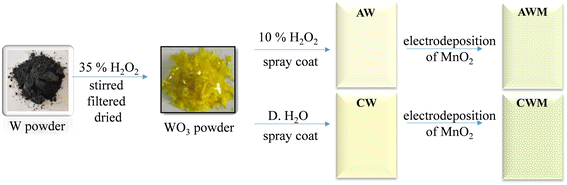 |
| | Fig. 1 Schematic representation of the fabrication process of MnO2 coated WO3 thin film electrodes. | |
The MnO2 layer was formed using a cyclic voltammetric method, as described by Kim et al.48 The experimental setup consisted of three electrodes: an Ag/AgCl reference electrode, a platinum counter electrode, and a working electrode made of FTO coated with WO3. The electrolyte solution is made by combining 2.5 mM MnSO4·H2O and 2.5 mM CH3COONa in an ethanol/water (35 mL/65 mL) solution. A series of 12 cycles was conducted, with each cycle consisting of repeating potential sweeps between 0.4 V and 1.3 V at a scan rate of 30 mV s−1. The films were then cleaned with ethanol and distilled water before annealing at 60 °C for two hours to produce the bilayer electrodes. These films were termed AWM and CWM to represent MnO2 overcoated AW and CW thin films. To compare, MnO2 films were also applied to the bare FTO employing the identical process.
For device fabrication, a gel electrolyte composed of PVA and Al3+ ions is utilized. To accomplish this, 0.1 grams of dehydrated Al2(SO4)3 and 1 gram of PVA are combined with 10 ml of distilled water. The mixture is then stirred at a temperature of 85 °C until a transparent gel solution is formed. To study the film properties, we utilized a bath containing 0.1 M Al2(SO4)3 in H2O.
2.3. Material characterization and electrochemical measurements
The morphological studies were conducted using X-ray diffraction (XRD, Bruker D8 ADVANCE), scanning electron microscopy (SEM, JEOL 5600 LV) and XPS (ULVAC PHI 5000 Versa Probe II, Al-Kα X-Ray source, 1486.6 eV). Both survey and high resolution spectra of the major elements were recorded and the peaks were fitted and analyzed using MultiPak® software. The C 1s peak at 284.8 eV was used as an internal energy reference. The thickness of the films was determined using a Dektak XT™ profilometer. The electrochromic and electrochemical performance tests were conducted utilizing a combination system consisting of a UV-Vis spectrometer (Ocean Optics USB4000-XR) and an electrochemical workstation (Metrohm micro-Autolab μ3AUT70904) that was coupled with NOVA™ software. The experimental setup for the three-electrode setup was completed using the WO3-coated FTO as the active electrode, a 0.1 M Al2(SO4)3 electrolyte bath, an Ag/AgCl reference, and a platinum wire counter electrode. The charge storage capacity and galvanostatic charge–discharge (GCD) were quantified using a PARSTAT 4000A high-precision workstation, which was equipped with the VersaStudio™ software. The EIS data were collected between 1 MHz and 0.1 Hz and fitted using ZSimpWin software. We performed all our electrochemical and electrochromic experiments by maintaining a temperature of around 20 °C.
3. Results and discussion
3.1. Structural and morphological studies
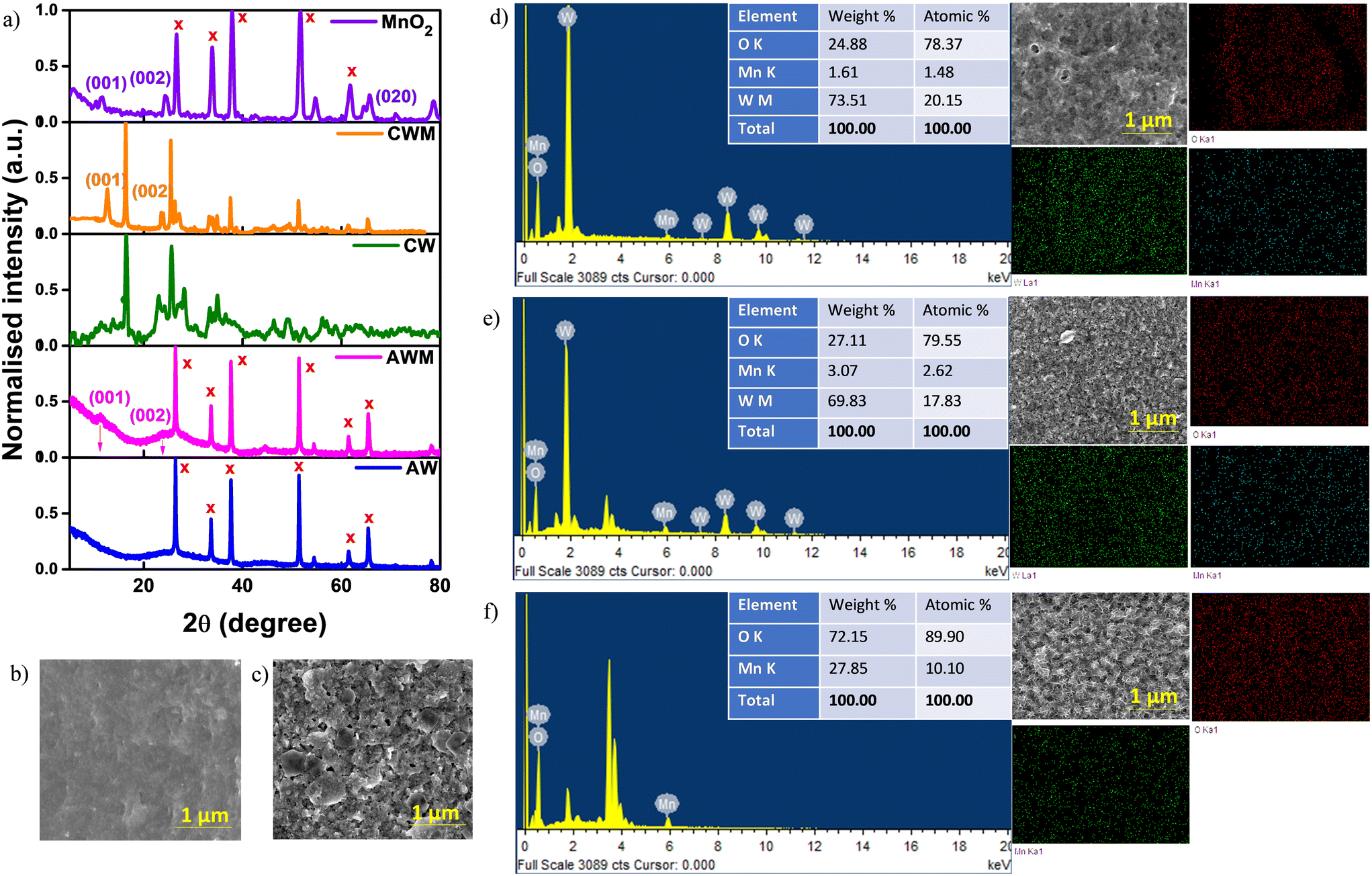
Fig. 2a displays the XRD patterns acquired for the fabricated coatings. The lack of any prominent peaks confirms the amorphous nature of AW. The XRD profile of CW exhibits peaks within the range of 10° to 60°, which correspond to the reflections from the (020), (120), (111), (121), (040), (200), (131), (231), and (222) planes. These peaks are consistent with those observed in the orthorhombic WO3·H2O phase (JCPDS#01-084-0886). The detected diffraction peaks at 2θ = 12° and 25° in AWM and CWM, respectively, correspond to the (110) and (220) planes of tetragonal MnO2 (JCPDS#00-044-0141). Fig. 2b–f show the surface morphologies of AW, CW, AWM, CWM, and MnO2 film on a bare FTO substrate. Although AW generally had a smooth and uniform appearance, CW films showed an irregular arrangement of rectangular sheets with varying sizes ranging from 10 to 500 nm. Using the fabrication procedure outlined in the experimental section, the thicknesses of the AW and CW films were determined to be 850 and 600 nm, respectively. An approximate thickness of 70 nm was determined for the MnO2 coating. The thickness profiles are presented in Fig. S1 (#ESI†). Upon deeper examination of AWM and CWM topologies, it becomes evident that the MnO2 overcoating preserves the original surface morphologies of the uncoated films. However, the effective surface areas are enhanced as a result of the lower grain size of MnO2. The MnO2 film shown in Fig. 2f had a distinct shape compared to AWM/CWM and displayed quasi-1D growth of the material. The disparity is ascribed to the distinct growth conditions stemming from the topography of the growth surfaces. The EDS mapping images are presented for the samples AWM, CWM, and MnO2 which indicate the uniform coating of MnO2 over the WO3 surfaces. The FTIR and Raman studies were conducted to check the deposition of MnO2 film on the FTO which is shown in Fig. S2.† The FTIR absorption bands at 400–800 cm−1 are related to Mn–O stretching vibrations, and the absorption bands at 1605, 1396, and 1106 cm−1 are ascribed to the bending vibrations of hydroxyl groups present on the surface of the MnO2 films,49 indicating the successful formation of MnO2 on the substrate. The Raman scattering spectrum shows a strong peak in the 500–680 cm−1 region which is attributed to the Mn–O stretching vibration, indicating the presence of MnO2 in the FTO/MnO2 film.49
 |
| | Fig. 2 a) XRD patterns of the films. SEM images of the films grown on FTO: b) AW and c) CW. EDS spectrum and elemental composition mapping: d) AWM, e) CWM, and f) MnO2. | |
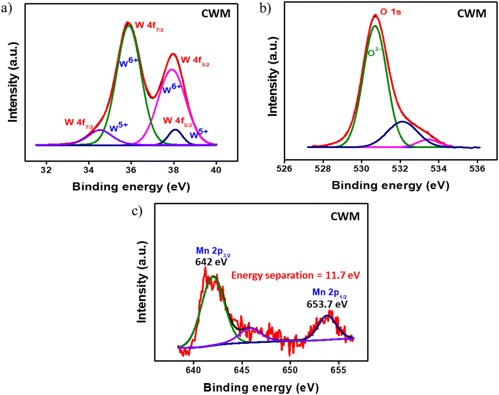
X-ray photoelectron spectroscopy (XPS) was conducted to analyze the elemental composition of the samples. The C 1s peak at 284.8 eV was utilized as the reference to correct for any energy shift. The survey spectra for both AWM, CWM, and bare MnO2 films are shown in Fig. S3 (#ESI†), which corroborate the presence of manganese, tungsten, and oxygen, with no detectable impurities. While the amorphous phase of WO3 does exhibit a high contrast electrochromism in the visible region, the specially designed crystalline phase is more desirable for manufacturing EESDs due to its greater charge storage capacity and broadband electrochromism.47,50 To prevent repetition, the CW and CWM data are provided in this section, whereas the AW and AWM data are referenced in the ESI,† except where there are particular requirements. Fig. 3a–c display the high-resolution spectra of the W 4f, O 1s, and Mn 2p regions. The deconvolution of the 4f doublet of tungsten (Fig. 3a) at 35.9 eV and 37.9 eV revealed a distinct pattern indicating the prevalence of W6+ states in the samples, accompanied by a small amount of W5+. From the area under the peaks, the ratio of W6+ to W5+ was estimated to be around 88:12 for AW and 83:17 for CW. The O 1s spectrum fitting depicted in Fig. 3b revealed three peaks at 530.7, 532.1, and 533.4 eV, which correspond to the metal–oxygen bonds (Mn–O–Mn and W–O–W), metal–hydroxide bond (Mn–OH and W–OH), and H–OH bond, respectively.51 The fitting of the Mn 2p spectrum is illustrated in Fig. 3c. The presence of the Mn4+ state was confirmed by 11.8 eV doublet energy separation between Mn 2p1/2 and Mn 2p3/2 states.52,53 Fig. S4 (#ESI†) shows the high-resolution data collected from AWM and bare MnO2 samples.
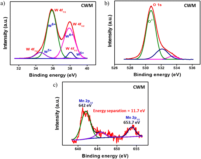 |
| | Fig. 3 Deconvoluted XPS spectra of CWM: a) W 4f, b) O 1s, and c) Mn 2p. | |
3.2. Electrochemical characterization
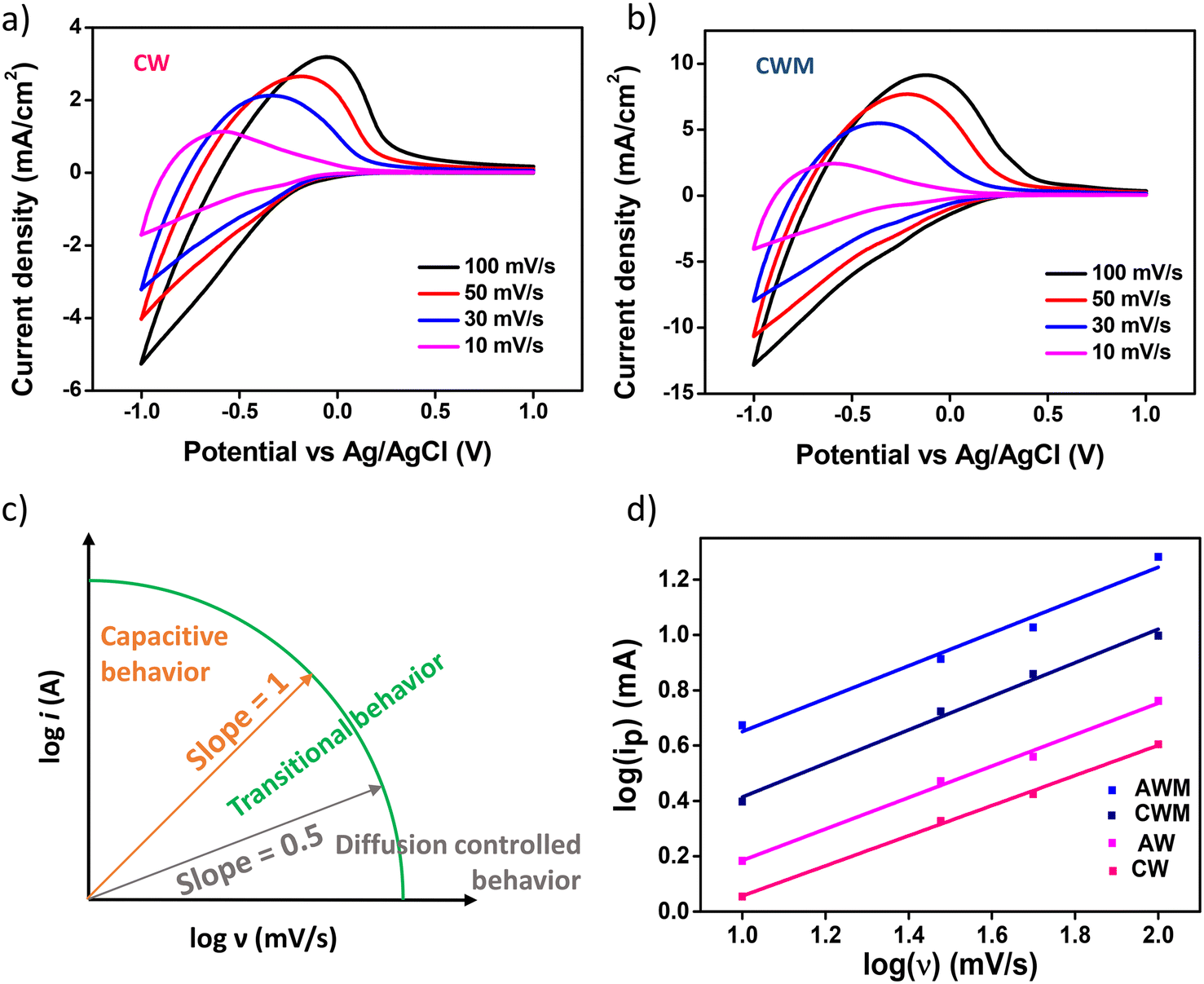
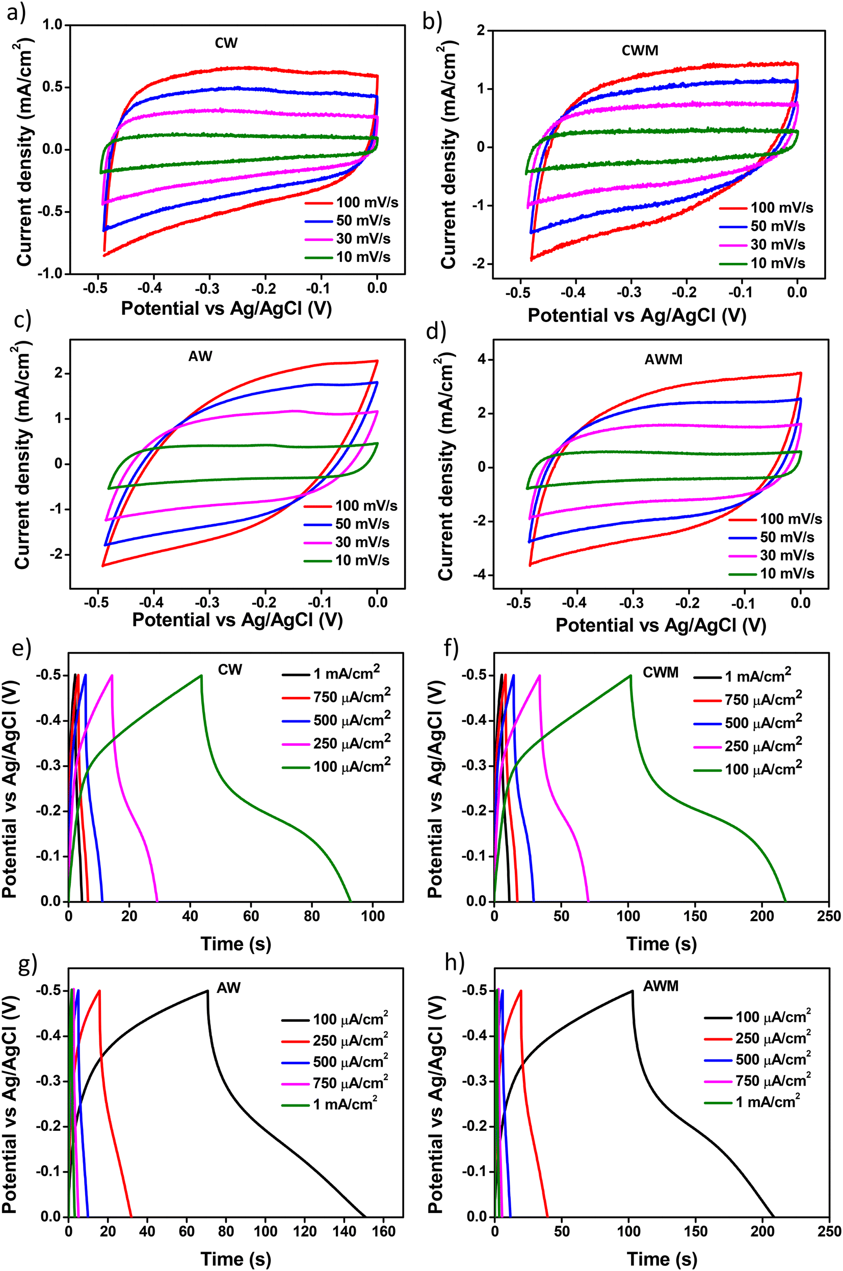
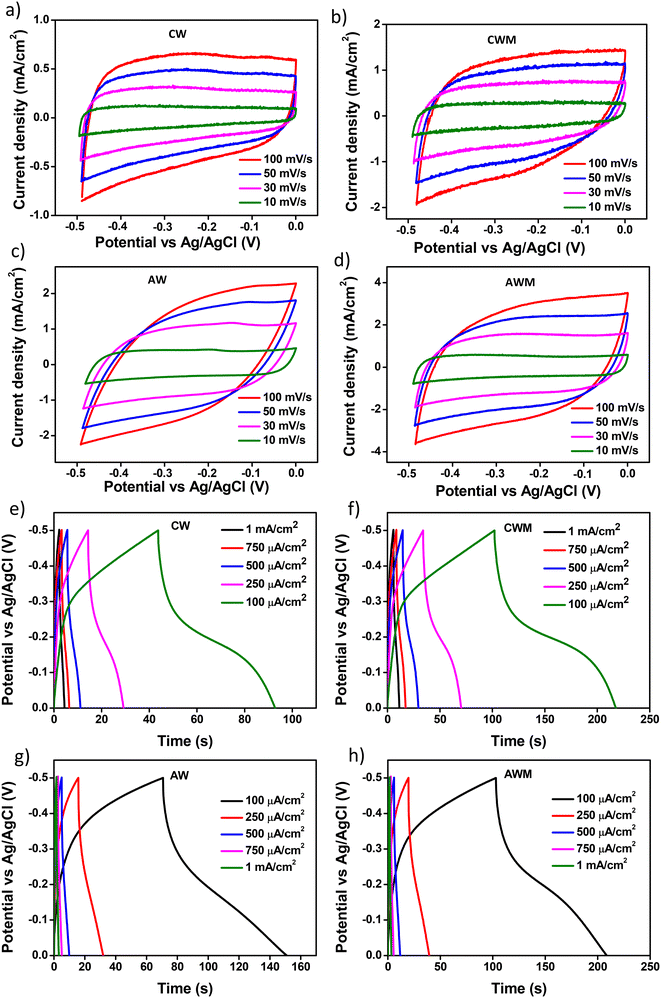
CV and GCD techniques were employed to analyze the ion intercalation/deintercalation processes with a three-electrode setup. The charge storage capacities of the electrodes were investigated by adjusting the scan rates from 10 to 100 mV s−1 within a potential window of ±1 V vs. Ag/AgCl, as depicted in Fig. 4a and b. An appreciable rise in the current density values was noted in the films following the application of MnO2 overcoating at all scan rates, thereby demonstrating the improved ability of the active electrode to store charges. Comparable findings were documented from the CV of AW and AWM, as depicted in Fig. S5 (#ESI†).
 |
| | Fig. 4 Cyclic voltammetry plots at variable scan rates of a) CW film and b) CWM film, c) illustration of power-law dependence of peak current with scan rate, and d) plots of peak current with scan rate of all the films. | |
In CV, the total current observed during a potential sweep can be described as the combination of the current resulting from the slow diffusion-controlled process (idiff) and the current required for charging the double layer formed at the interface between the electrolyte and the electrode (icap). The equation can be expressed mathematically as a power-law dependence;
| | | i(v) = idiff + icap = avb | (1) |
| | | logi(v) = loga + blogv | (2) |
where
i is the current,
v is the scan rate, and
a and
b are constants.
54 The value of “
b” can be determined from the slope of the log
i(
v)
vs. log(
v) plot. The
b-value indicates the nature of the electrochemical processes occurring and presents two well-established scenarios. At
b = 1, the peak current exhibits a linear relationship with the scan rate, suggesting that rapid events such as surface redox reactions and the charging/discharging of the EDLC play a significant role.
55 When the value of
b is 0.5, it indicates that a slow diffusion-controlled faradaic process is predominant. The intermediate values ranging from 0.5 to 1 signify a transitional behavior between pseudocapacitive and battery-like properties.
56Fig. 4c visually depicts the electrochemical behavior associated with the
b-value. The
b values for the CW, CWM, AW, and AWM films were measured to be 0.54, 0.61, 0.55, and 0.59, respectively, as depicted in
Fig. 4d. Based on these results, it may be inferred that the electrode composition exhibits pseudocapacitive or battery-like behaviour, with diffusion-controlled processes being the dominant factor. Fig. S6
† shows the respective contribution from the diffusion-controlled and capacitive current contribution for the crystalline and amorphous WO
3 and WO
3/MnO
2 films at different scan rates. In all these electrodes, the capacitive process is found to be highly dominant. As observed in Fig. S6b and S6d,
† the MnO
2 modification resulted in an increased contribution from the capacitive process compared to the bare WO
3 films.
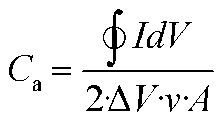
A more realistic range of potential from 0 V to −0.5 V versus Ag/AgCl was adopted to determine the areal capacitance of the films. The acquired CVs are depicted in Fig. 5a–d. The areal and volumetric capacitances can be determined from the CV charts using the following well-established equation,57
| |  | (3) |
where ∮
IdV represents the area under the CV curve, Δ
V is the potential window in volts,
A is the coating area on the electrode, and
ν is the scan rate. The computed values are documented in
Table 1. The data demonstrate a significant increase in the storage capacity of the WO
3 films upon MnO
2 overcoating, especially for the amorphous films. At
ν = 100 mV s
−1 the
Ca value of AWM increased to 24.6 mF cm
−2 from 6.3 mF cm
−2 of AW, exhibiting ∼4× enhancement. The crystalline phase had approximately 1.4× increase (11.5–16.1 mF cm
−2) post-MnO
2 coating, indicating less dependency. Such enhancement can be attributed to the increase in the surface area due to the lower grain size of MnO
2, resulting in more active electrochemical sites. Additionally, the creation of heterojunctions also contributes to the activation energy for ion intercalation/deintercalation.
38 The concentration of
Ca drops as the scan rate increases. The higher concentration of
Ca at a lower scan rate indicates that there is ample time for the gradual diffusion of Al
3+ ions on the electrode material.
 |
| | Fig. 5 CV of films at varying scan rates: a) AW, b) AWM, c) CW, and d) CWM; GCD curves of samples at different current densities: e) CW, f) CWM, g) AW, and h) AWM. | |
Table 1 Areal capacitance values for the films
| Scan rate (mV s−1) |
CW film (mF cm−2) |
CWM film (mF cm−2) |
AW film (mF cm−2) |
AWM film (mF cm−2) |
| 10 |
24.6 |
31.2 |
23.1 |
64.5 |
| 30 |
16.7 |
27.4 |
13.7 |
42.2 |
| 50 |
15.5 |
25.2 |
10.5 |
34.4 |
| 100 |
11.5 |
16.1 |
6.3 |
24.6 |
Fig. 5e–h display the GCD profiles of all four films. Since the charging and discharging intervals for each sample were almost the same, it may be inferred that the electrochemical reactions exhibit a high coulombic efficiency. The discharge curve of the samples significantly diverges from the triangular form, indicating that redox processes are involved.58 Such observations confirmed the presence of faradaic electron transport and pseudocapacitance characteristics.59 The crystalline sample exhibited relatively higher faradaic contribution, the mechanism of which was described in detail in one of our earlier studies.36 The volumetric capacitance values of all the thin films were calculated from GCD using the following equation:
| | 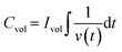 | (4) |
where
Ivol is the discharge current,
t is the discharge time, and
V is the potential range. From the GCD curves, the value of
Cvol is calculated and is tabulated in
Table 2. Crystalline films showed a greater
Cvol than amorphous films due to their lower thickness. The maximum
Cvol was measured to be 341.0 F cm
−3 for the CWM sample with a discharge rate of 0.1 mA cm
−2. Nevertheless, when considering a practical discharge rate of 1.0 mA cm
−2, CWM demonstrated a
Cvol of 171.0 F cm
−3, which surpasses the
Cvol of AWM with a significantly lower discharge rate of 0.3 mA cm
−2. These observations indicate that the volume-normalized charge storage capacity of CWM is the highest among all the samples. Furthermore,
Table 2 shows that the crystalline films have superior capacitance retention as the discharge rate increases. When comparing the capacitance retention of CWM and AWM, it was found that CWM had a retention rate of roughly 50% (from 341.0 F cm
−3 to 171.0 F cm
−3) for discharge rates of 0.1 mA cm
−2 and 1.0 mA cm
−2, whereas AWM only showed a retention of 15%.
Table 2 Volumetric capacitance values for the films
| Discharge current (mA cm−2) |
CW film (mF cm−3) |
CWM film (mF cm−3) |
AW film (mF cm−3) |
AWM film (mF cm−3) |
| 0.1 |
162 |
341 |
189 |
229 |
| 0.3 |
138 |
322 |
114 |
129 |
| 0.5 |
92 |
223 |
59 |
64 |
| 0.75 |
81 |
195 |
44 |
45 |
| 1 |
72 |
171 |
37 |
35 |
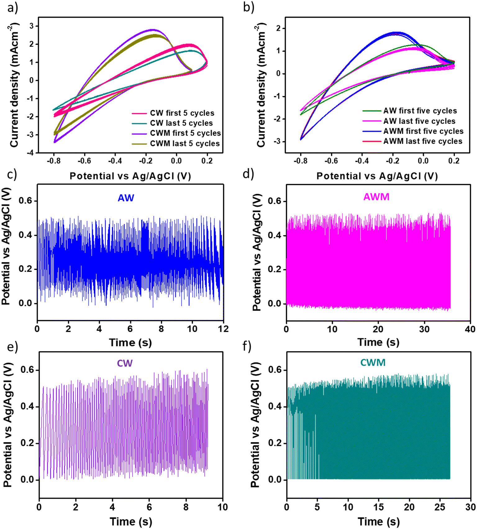
The cyclic stability of the films was determined by conducting a continuous 500 sweep from −0.8 to 0.2 V with respect to Ag/AgCl. The region bounded by the oxidation and reduction paths, as depicted in Fig. 6a and b, provides a quantitative measure of the overall charge implicated in the redox process. The enhancement of the charging and discharging capabilities of crystalline and amorphous materials is clearly evident due to the MnO2 overcoating. In addition, the coated films demonstrated remarkable cyclic stability, as indicated by the CV plot for the last five cycles. The cyclic stability was also confirmed using GCD cycles (Fig. 6c–f), where we performed the stability tests in 0 to 0.5 V with respect to Ag/AgCl for 500 sweeps. The initial cycle capacitance and that from the last cycle were calculated and it is found that the films with MnO2 overcoating show ∼100% retention while the uncoated films show approximately 50% reduction of capacitance. The coated films show much better charge–discharge stability even after 500 continuous sweeps.
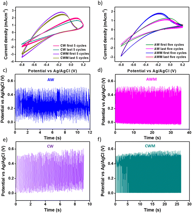 |
| | Fig. 6 Stability tested from CV cycles at a scan rate of 50 mV s−1 for 500 cycles of all four films: a) first and last five cycles of CW and CWM, b) first and last five cycles of AW and AWM, stability cycles tested from GCD at a scan rate of 1 mA cm−2 for 500 cycles of all four films: c) AW, d) AWM, e) CW, and f) CWM films. | |
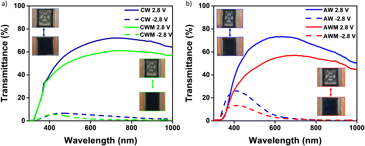
3.3. Electrochromic performance assessment
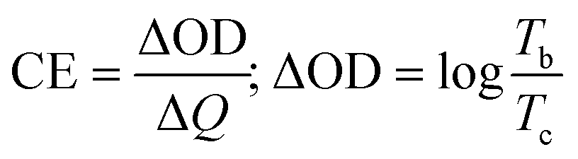
The films were used to fabricate four different ECDs using PVA/Al3+ gel electrolyte (GE). The EC performance of the devices was evaluated by subjecting them to reversible potentials of ±2.8 V across the wavelength range of 300 to 1000 nm. Fig. 7a and b display the full transmittance spectra of the devices in both the bleached and colored states and the corresponding photographs are shown in the inset. The data indicates that the application of MnO2 coating resulted in a small reduction in transmittance in the bleached ECDs, causing them to exhibit a slightly yellow shade due to their anodic electrochromism. Both devices exhibited exceptional visible and infrared cut-off performance upon coloration above the 600 nm wavelength threshold. The amorphous devices had a higher peak visual contrast of 70% at 650 nm compared to the crystalline phase, which had a peak contrast of 63% at 650 nm. The coloration efficiency (CE, cm2 C−1) at a certain wavelength, which is a figure of merit for ECDs, can be computed by the following equation,| |  | (5) |
The equation represents the relationship between ΔOD (change in optical density), ΔQ (amount of charge introduced), and % transmittance at bleached (Tb) and colored (Tc) states.60 The ΔQ values were calculated by analyzing the chronoamperometry graphs presented in Fig. S7 (#ESI†). By integrating these plots with the colored/bleached transmittance plot, the CE values were derived. The values obtained from all four devices are enumerated in Table 3. The MnO2 coating led to a general improvement in the CE values for both amorphous (47–52 cm2 C−1) and crystalline phases (22–27 cm2 C−1) at 650 nm. The amorphous phase has significantly greater CE values compared to the crystalline state. It is important to highlight that, as stated in eqn (5), a reduction in the CE value indicates that a higher amount of stored charges is needed to accomplish the same level of optical density change. Hence, the WO3 crystalline phase is typically more favorable for simultaneous charge storage and EC coloration.
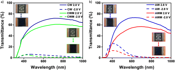 |
| | Fig. 7 Transmittance spectra of the devices (inset: digital photographs at the bleached and colored states): a) devices CW and CWM (upper-left: CW, lower-right: CWM), b) devices AW and AWM (upper-left: AW, lower-right: AWM). | |
Table 3 Comparison of performance parameters of all devices
|
|
Device CW |
Device CWM |
Device AW |
Device AWM |
| Transmittance contrast (%) |
63.2 |
57.9 |
69.7 |
55.6 |
| Coloration efficiency (cm2 C−1) @ 650 nm |
21.8 |
27.2 |
47.3 |
51.7 |
| Switching time [tc/tb] |
7 s/11 s |
5 s/9 s |
7 s/11 s |
7 s/15 s |
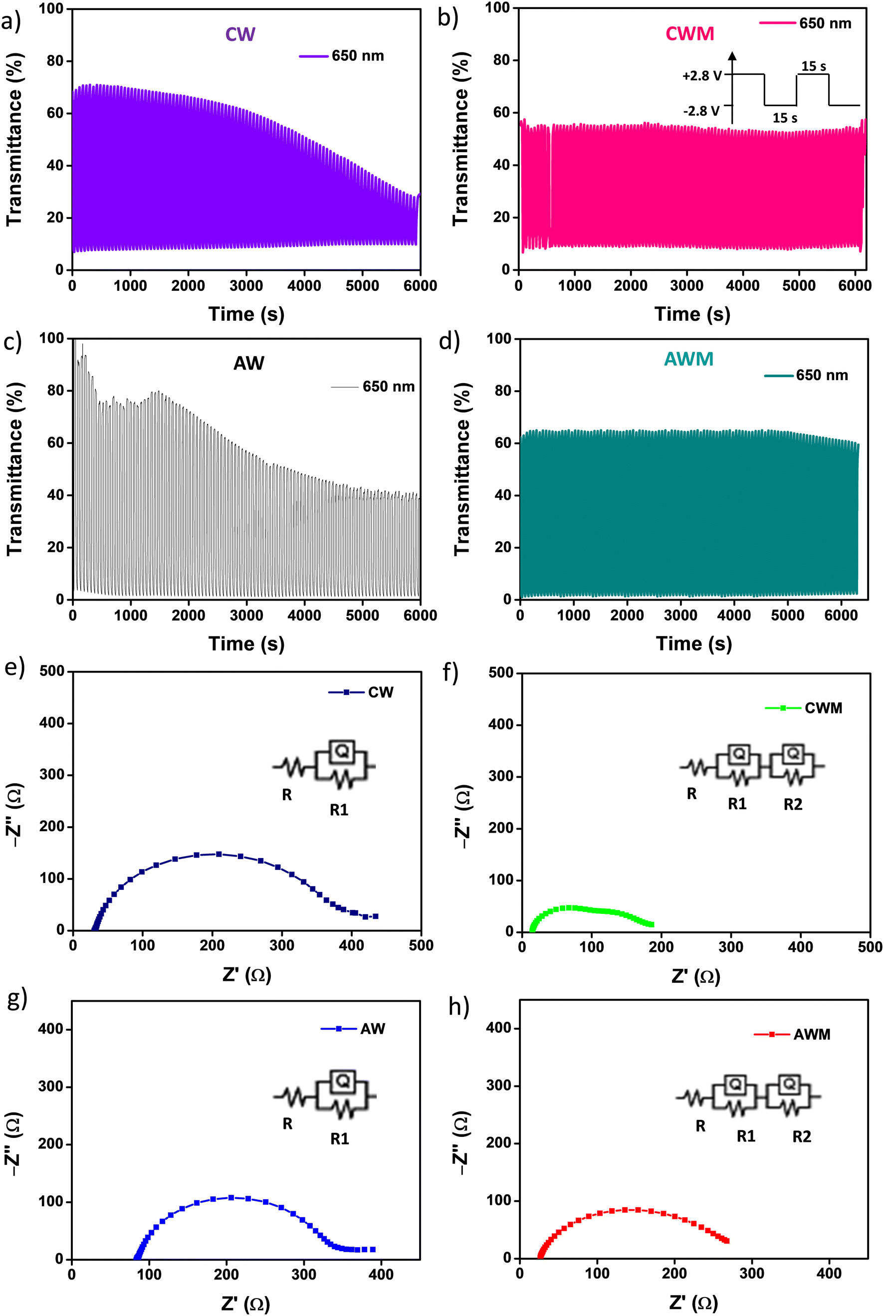
Cyclic stability is a critical performance metric for ECDs. Fig. 8a and d depict the cyclic stability of all four devices over 200 cycles with a 15 s voltage pulse. The ECDs with CW and AW electrodes exhibited a consistent decrease in transmittance after a few initial cycles, and a 71 and 57% reduction in optical transmittance is noted across the full 200 cycles. On the other hand, CWM and AWM showed almost no reduction, indicating highly improved cyclic stability. The T90 coloration and bleaching response times of all the films were calculated from the single charge–discharge cycles, as shown in Fig. S8 (#ESI†), and recorded in Table 3. Although CWM showed a slight improvement in the response times, those are practically comparable to other devices. A comparison of the performance of the ECD against the results from previous literature reports is shown in Table 4 (Fig. S9†). To address the crucial circuit factors associated with ECD operation, we utilized the three-electrode EIS technique within the frequency range of [0.1 Hz–1 MHz]. Fig. 8e and g display Nyquist plots for CW and AW, showing a solitary depressed semicircle at higher frequencies and a diffusion-limited impedance tail in the low-frequency range. The semicircle spectra can be easily fitted using a modified Randle's equivalent circuit that consists of a single RC loop (shown in the inset). In this case, R represents the overall resistance of the cell. R1 specifically refers to the resistance associated with charge transfer at the interface between the semiconductor and electrolyte. Q1 indicates the capacitance related to the space charge. In the case of CWM and AWM (Fig. 8f and h), a second R2–Q2 loop is included (as shown in the inset), where R2 and Q2 reflect the charge transfer resistance and capacitance contributed by the MnO2 overcoating. The data obtained from the analysis is displayed in Table 5, illustrating a substantial drop in the charge transfer resistances at the MnO2/WO3 contact compared to the bare WO3/electrolyte interface. The decrease in charge transfer resistances is associated with the changes in activation energy of the electrochemical process, as described by the Arrhenius equation,61
where
k represents the rate constant of the electrochemical process,
Rct represents the charge transfer resistance,
A is the pre-exponential factor,
Ea represents the activation energy,
Rg is the gas constant, and
T is the temperature. Consequently, the MnO
2 overcoating served as a protective barrier between the electrolyte and WO
3 films, simultaneously lowering the interfacial activation energy for charge transfer to WO
3, resulting in enhanced electrochemical stability.
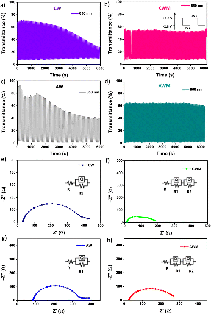 |
| | Fig. 8 Cyclic stability of the devices for 200 cycles at 650 nm in a 15 s pulse width: a) device CW, b) device CWM, c) device CW, d) device AWM; Nyquist plots in the 0.1 Hz to 1 MHz range for e) CW, f) CWM, g) AW, and h) AWM. | |
Table 4 Comparison with previous literature reports
| Reference |
System |
Materials used |
Electrochromic |
Electrochemical |
Retention |
| Zhao et al.62 |
EESD |
Cathode: WO3 |
t
b/tc = 9.37/5.19 s |
10.69 mF cm−2 @ 0.1 mA cm−2 |
95.9% @ 1000 cycles |
| Anode: MnO2 |
η = 85.36 cm2 C−1 |
| Shinde et al.63 |
SC device |
Cathode: WO3 |
NA |
103 F g−1 @ 5 mV s−1 |
95% @ 2500 cycles |
| Anode: WO3–MnO2 |
| Xi et al.64 |
EESW |
Cathode: Mo-doped WO3 |
t
b/tc = 4/4.9 s |
19.1 mF cm−2 @ 0.1 mA cm−2 |
— |
|
η = 84.3 cm2 C−1 |
| Anode: MnO2 |
| Lee et al.30 |
EESD |
Cathode: TiO2 |
t
b/tc = 2.66/2.72 s |
26.0 mF cm−2 @ 0.2 mA cm−2 |
— |
| Anode: MnO2/Ni(OH)2 |
η = 34 cm2 C−1 |
| Wang et al.65 |
EESD |
Cathode: P2W17O6111−/TiO2 |
t
b/tc = 1.9/2.1 s |
10.9 mF cm−2 @ 0.1 mA cm−2 |
— |
|
η = 171 cm2 C−1 |
| Anode: MnO2 |
| Cai et al.66 |
MnO2 dual electrode |
Anode: MnO2 |
t
b/tc = 45/45 s |
570 mA h m−2 @ 0.1 mA cm−2 |
— |
| Cathode: Cu frame |
OM = 64% @ 550 nm |
| Our work |
ECD |
Cathode: aWO3–MnO2 |
t
b/tc = 8/7 s |
21.08 mF cm−2 @ 0.25 mA cm−2 |
100% @ 500 cycles |
|
η = 51.7 cm2 C−1 |
| Anode: FTO |
Table 5 Fitting parameters of all the devices
|
|
R (Ω) |
R
1 (Ω) |
R
2 (Ω) |
Q
1 (F) |
Q
1 n |
Q
2 (F) |
Q
2 n |
| CW |
31.4 |
340.4 |
— |
2.3 × 10⁻³ |
0.8 |
— |
— |
| CWM |
14.5 |
51.0 |
40.3 |
0.4 × 10⁻³ |
0.8 |
1.7 × 10⁻⁵ |
0.8 |
| AW |
84.5 |
268.6 |
— |
1.8 × 10⁻⁵ |
0.8 |
— |
— |
| AWM |
26.5 |
124.5 |
119.7 |
2.7 × 10⁻³ |
0.8 |
8.2 × 10⁻⁵ |
0.8 |
4. Conclusion
A bilayer structure was developed using sol–gel and electrochemical routes to coat an ultrathin layer of MnO2 onto both amorphous and crystalline WO3 films. The structural and compositional investigations confirmed the phase purity and chemical homogeneity of the materials. With an Al3+ ion-containing gel electrolyte, the electrochemical and electrochromic performance of these electrodes was examined. The CV measurements revealed a notable enhancement in the storage capacity of the WO3 films when coated with MnO2, particularly for the amorphous films. At ν = 100 mV s−1, the Ca value of AWM increased to 24.6 mF cm−2 from 6.3 mF cm−2 of AW, showing nearly a 4-fold enhancement. The crystalline phase experienced a roughly 1.4-fold rise (from 11.5 mF cm−2 to 16.1 mF cm−2) after the MnO2 coating. Nevertheless, the volume normalized charge storage capacity of CWM was found to be the highest for all the electrodes. A peak charge storage capacity of 341.0 F cm−3 was achieved at a charging rate of 0.1 mA cm−2. MnO2 overcoating improved the coloration efficiency of the ECDs for both amorphous (47–52 cm2 C−1) and crystalline phases (22–27 cm2 C−1), measured at 650 nm. Furthermore, the bilayered electrodes demonstrated exceptional stability across 200 cycles, with virtually no reduction in the optical transmittance contrast.
Data availability
The raw/processed data required to reproduce these findings cannot be shared at this time as the data also forms part of an ongoing study. However, whole or part of the data will be made available on specific request. Some of the data supporting this article have been included as part of the ESI.†
Conflicts of interest
There are no conflicts to declare.
Acknowledgements
This work is supported by the Science and Engineering Research Board (SERB), Govt. of India through the grant CRG/2021/006282 (Core Research Grant). RV thanks the University Grants Commission (UGC-India) for her fellowship support. The authors extend their gratitude to Mr. Peer Muhammed and Mr. Harish Raj for their experimental help.
References
- G. F. Zhao, W. Q. Wang, X. L. Wang, X. H. Xia, C. D. Gu and J. P. Tu, J. Mater. Chem. C, 2019, 7, 5702–5709 RSC.
- M. Qiu, P. Sun, L. Shen, K. Wang, S. Song, X. Yu, S. Tan, C. Zhao and W. Mai, J. Mater. Chem. A, 2016, 4, 7266–7273 RSC.
- Z. Bi, X. Li, X. He, Y. Chen, X. Xu and X. Gao, Sol. Energy Mater. Sol. Cells, 2018, 183, 59–65 CrossRef CAS.
- P. Sun, Z. Deng, P. Yang, X. Yu, Y. Chen, Z. Liang, H. Meng, W. Xie, S. Tan and W. Mai, J. Mater. Chem. A, 2015, 3, 12076–12080 RSC.
- P. Yang, P. Sun, Z. Chai, L. Huang, X. Cai, S. Tan, J. Song and W. Mai, Angew. Chem., Int. Ed., 2014, 53, 11935–11939 CrossRef CAS PubMed.
- B. Deb, S. Desai, G. U. Sumanasekera and M. K. Sunkara, Nanotechnology, 2007, 18, 285501 CrossRef.
- W. Cheng, Y. Ju, P. Payamyar, D. Primc, J. Rao, C. Willa, D. Koziej and M. Niederberger, Angew. Chem., Int. Ed., 2015, 54, 340–344 CrossRef CAS PubMed.
- P. M. Rao, L. Cai, C. Liu, I. S. Cho, C. H. Lee, J. M. Weisse, P. Yang and X. Zheng, Nano Lett., 2014, 14, 1099–1105 CrossRef CAS PubMed.
- R. Abe, K. Shinmei, N. Koumura, K. Hara and B. Ohtani, J. Am. Chem. Soc., 2013, 135, 16872–16884 CrossRef CAS PubMed.
- M. R. Waller, T. K. Townsend, J. Zhao, E. M. Sabio, R. L. Chamousis, N. D. Browning and F. E. Osterloh, Chem. Mater., 2012, 24, 698–704 CrossRef CAS.
- S. Wang, H. Xu, T. Hao, M. Xu, J. Xue, J. Zhao and Y. Li, Appl. Surf. Sci., 2022, 577, 151889 CrossRef CAS.
- L. Manjakkal, L. Pereira, E. Kumi Barimah, P. Grey, F. F. Franco, Z. Lin, G. Jose and R. A. Hogg, Prog. Mater. Sci., 2024, 142, 101244 CrossRef CAS.
- Y. Shi, M. Sun, Y. Zhang, J. Cui, Y. Wang, X. Shu, Y. Qin, H. H. Tan, J. Liu and Y. Wu, Sol. Energy Mater. Sol. Cells, 2020, 212, 110579 CrossRef CAS.
- W. Li, J. Zhang, Y. Zheng and Y. Cui, Sol. Energy Mater. Sol. Cells, 2022, 235, 111488 CrossRef CAS.
- G. Mineo, E. Bruno and S. Mirabella, Nanomaterials, 2023, 13, 1418 CrossRef CAS PubMed.
- H. Park, D. S. Kim, S. Y. Hong, C. Kim, J. Y. Yun, S. Y. Oh, S. W. Jin, Y. R. Jeong, G. T. Kim and J. S. Ha, Nanoscale, 2017, 9, 7631–7640 RSC.
- J. W. Kim and J. M. Myoung, Adv. Funct. Mater., 2019, 29, 1–9 Search PubMed.
- Q. Zhao, Y. Fang, K. Qiao, W. Wei, Y. Yao and Y. Gao, Sol. Energy Mater. Sol. Cells, 2019, 194, 95–102 CrossRef CAS.
- D. Kim and Y. Choi, Appl. Sci., 2021, 11, 4956 CrossRef CAS.
- A. W. Lang, A. M. Österholm and J. R. Reynolds, Adv. Funct. Mater., 2019, 29, 1–11 Search PubMed.
- C. K. Wang, D. R. Sahu, S. C. Wang, C. K. Lin and J. L. Huang, J. Phys. D: Appl. Phys., 2012, 45, 225303 CrossRef.
- P. Judeinstein, R. Morineau and J. Livage, Solid State Ionics, 1992, 51, 239–247 CrossRef CAS.
- Z. Wang, X. Zhang, H. Zhang, F. Ge, Q. Wang, C. Zhang, G. Xu, J. Gao, A. A. Rogachev and H. Cao, Adv. Mater. Interfaces, 2022, 9, 7–13 Search PubMed.
- W. Q. Wang, Z. J. Yao, X. L. Wang, X. H. Xia, C. D. Gu, J. P. Tu, Z. J. Yao, X. L. Wang, X. H. Xia, C. D. Gu and J. P. Tu, J. Colloid Interface Sci., 2019, 535, 300–307 CrossRef CAS PubMed.
- K. Ahmad, M. A. Shinde, G. Song and H. Kim, Ceram. Int., 2021, 47, 34297–34306 CrossRef CAS.
- M. Wang, Y. He, M. Da Rocha, A. Rougier and X. Diao, Sol. Energy Mater. Sol. Cells, 2021, 230, 111239 CrossRef CAS.
- J. C. Expósito-Gálvez, L. Hromadko, M. Sepúlveda, F. J. Peón-Díaz, S. D. Coria-Quiñones, O. Jiménez-Sandoval, J. M. Macak and G. Oskam, Electrochim. Acta, 2024, 474, 143545 CrossRef.
- X. Li, Z. Li, W. He, H. Chen, X. Tang, Y. Chen and Y. Chen, Coatings, 2021, 11, 2–11 Search PubMed.
- S. W. Siyuan Yang, J. Cao, W. Xu, X. He, Z. Wang, Z. Zhang, Z. Sun and H. Zhang, ACS Appl. Nano Mater., 2022, 5, 16544–16552 CrossRef.
- Y. H. Lee, J. Y. Park, K. S. Ahn and Y. E. Sung, J. Alloys Compd., 2022, 923, 166446 CrossRef CAS.
- K. Zhang, X. Han, Z. Hu, X. Zhang, Z. Tao and J. Chen, Chem. Soc. Rev., 2015, 44, 699–728 RSC.
- B. Saravanakumar, K. K. Purushothaman and G. Muralidharan, CrystEngComm, 2014, 16, 10711–10720 RSC.
- C. X. Guo, G. Yilmaz, S. Chen, S. Chen and X. Lu, Nano Energy, 2015, 12, 76–87 CrossRef CAS.
- S. Sajitha, U. Aparna and B. Deb, Adv. Mater. Interfaces, 2019, 6, 1–9 CrossRef.
- R. Ravi, S. Surendren and B. Deb, Surf. Interfaces, 2021, 22, 100860 CrossRef CAS.
- Y. Zhang, X. Jing, Q. Wang, J. Zheng, H. Jiang and C. Meng, Dalton Trans., 2017, 46, 15048–15058 RSC.
- P. T. G. Gayathri, S. Sajitha, I. Vijitha, S. S. Shaiju, R. Remya and B. Deb, Electrochim. Acta, 2018, 272, 135–143 CrossRef CAS.
- C. C. Wei, P. H. Lin, C. E. Hsu, W. Bin Jian, Y. L. Lin, J. T. Chen, S. Banerjee, C. W. Chu, A. P. Khedulkar, R. A. Doong and K. Tsukagoshi, Cell Rep. Phys. Sci., 2024, 5, 101836 CrossRef CAS.
- S. Zhang, J. He, J. Zheng, C. Huang, Q. Lv, K. Wang, N. Wang and Z. Lan, J. Mater. Chem. A, 2017, 5, 2045–2051 RSC.
- T. Koketsu, J. Ma, B. J. Morgan, M. Body, C. Legein, W. Dachraoui, M. Giannini, A. Demortière, M. Salanne, F. Dardoize, H. Groult, O. J. Borkiewicz, K. W. Chapman, P. Strasser and D. Dambournet, Nat. Mater., 2017, 16, 1142–1148 CrossRef CAS PubMed.
- M. C. Lin, M. Gong, B. Lu, Y. Wu, D. Y. Wang, M. Guan, M. Angell, C. Chen, J. Yang, B. J. Hwang and H. Dai, Nature, 2015, 520, 325–328 CrossRef PubMed.
- K. Li, Y. Shao, S. Liu, Q. Zhang, H. Wang, Y. Li and R. B. Kaner, Small, 2017, 13, 1–10 CAS.
- S. Zhang, S. Cao, T. Zhang, A. Fisher and J. Y. Lee, Energy Environ. Sci., 2018, 11, 2884–2892 RSC.
- Y. Tian, W. Zhang, S. Cong, Y. Zheng, F. Geng and Z. Zhao, Adv. Funct. Mater., 2015, 25, 5833–5839 CrossRef CAS.
- W. Mengying, Y. Hang, W. Xu and D. Xungang, Sol. Energy Mater. Sol. Cells, 2021, 230, 111196 CrossRef.
- G. P. T. Ganesh and B. Deb, Adv. Mater. Interfaces, 2017, 4, 1700124 CrossRef.
- P. T. G. Gayathri, S. S. Shaiju, R. Remya and B. Deb, Mater. Today Energy, 2018, 10, 380–387 CrossRef.
- G. Kim, I. Ryu and S. Yim, Sci. Rep., 2017, 7, 1–9 CrossRef PubMed.
- H. Li, Y. He, V. Pavlinek, Q. Cheng, P. Saha and C. Li, J. Mater. Chem. A, 2015, 3, 17165–17171 RSC.
- R. Venugopal, G. Prabhu, T. Ganesh, B. B. Swayamprabha, A. Philomina, L. V. Kulathur, N. Dev and B. Deb, Chem. Eng. J., 2021, 423, 130306 CrossRef CAS.
- M. Toupin, T. Brousse and D. Be, Chem. Mater., 2004, 16, 3184–3190 CrossRef CAS.
- M. A. Stranick and M. A. Stranick, Surf. Sci. Spectra, 2015, 6, 31 CrossRef.
- A. L. M. Reddy, M. M. Shaijumon, S. R. Gowda and P. M. Ajayan, Nano Lett., 2009, 9, 1002–1006 CrossRef CAS PubMed.
- J. Liu, J. Wang, C. Xu, H. Jiang, C. Li, L. Zhang, J. Lin and Z. X. Shen, Adv. Sci., 2017, 5, 1700322 CrossRef PubMed.
- J. Come, P.-L. Taberna, S. Hamelet, C. Masquelier and P. Simon, J. Electrochem. Soc., 2011, 158, A1090 CrossRef CAS.
- M. Sathiya, A. S. Prakash, K. Ramesha, J. À. M. Tarascon and A. K. Shukla, J. Am. Chem. Soc., 2011, 133, 16291–16299 CrossRef CAS PubMed.
- A. Laheäär, P. Przygocki, Q. Abbas and F. Béguin, Electrochem. Commun., 2015, 60, 21–25 CrossRef.
- J. Pan, R. Zheng, Y. Wang, X. Ye, Z. Wan, C. Jia, X. Weng, J. Xie and L. Deng, Sol. Energy Mater. Sol. Cells, 2020, 207, 110337 CrossRef CAS.
- Y. Gogotsi and R. M. Penner, ACS Nano, 2018, 12, 2081–2083 CrossRef CAS PubMed.
- D. D. Yao, R. A. Rani, A. P. O'Mullane, K. Kalantar-Zadeh and J. Z. Ou, J. Phys. Chem. C, 2014, 118, 10867–10873 CrossRef CAS.
- M. A. Zabara, G. Katlrcl and B. Ülgüt, J. Phys. Chem. C, 2022, 126, 10968–10976 CrossRef CAS.
- L. Zhao, Z. Chen, Y. Q. Peng, L. Yang, J. Ai, J. Zhou and L. Miao, Sustainable Mater. Technol., 2022, 32, 445 Search PubMed.
- P. A. Shinde, V. C. Lokhande, A. M. Patil, T. Ji and C. D. Lokhande, Int. J. Hydrogen Energy, 2018, 43, 2869–2880 CrossRef CAS.
- S. Xi, Y. Chen, S. Jia, X. Gao, X. Li, Z. Bi and X. Guo, Chem. Eng. J., 2019, 370, 1459–1466 CrossRef CAS.
- S. M. Wang, Y. H. Jin, T. Wang, K. H. Wang and L. Liu, J. Materiomics, 2023, 9, 269–278 CrossRef.
- J. Wang, Y. Zhou, Y. Lv, J. F. Feng, Z. Wang and G. Cai, Small, 2024, 20, 2310229 CrossRef CAS PubMed.
|
| This journal is © The Royal Society of Chemistry 2024 |
Click here to see how this site uses Cookies. View our privacy policy here. 
 Open Access Article
 This Open Access Article is licensed under a Creative Commons Attribution-Non Commercial 3.0 Unported Licence
 *ab
*ab