DOI:
10.1039/D3MA00678F
(Paper)
Mater. Adv., 2024,
5, 1576-1587
Fast response and multi-color photodetection in p-type Cu:CdS thin films†
Received
8th September 2023
, Accepted 15th December 2023
First published on 10th January 2024
Abstract
We present an analysis of p-type CdS thin films deposited on glass substrates with the addition of Cu dopants. Subsequently, we explore the photodetection capabilities of the Cu:CdS/FTO heterostructure. CdS, a popular and economical photo-conducting material operating within the spectral range similar to that of the human eye, is the subject of our investigation in this work. Multicolor detection with improved sensitivity, speed, and stability remains relatively unexplored in CdS-based photodetectors. Also, the industrially beneficial spray pyrolysis technique is employed for the fabrication. Furthermore, we address the shortcomings of photodetection in the metal–semiconductor–metal structure by implementing a simple vertical heterojunction structure, p-Cu:CdS/n-FTO. Among the various Cu-doped CdS films evaluated for their optoelectronic applications, we have determined that the CdS film with a 10% Cu concentration is optimal for photodetection purposes. Low density of sulfur vacancies, proper chemical composition, and good crystallinity observed for the 10 at% Cu doped CdS film supported the excellent performance of the p-Cu0.1Cd0.9S/n-FTO photodetector.
Introduction
Photodetectors find a wide range of commercial applications in the fields of photovoltaics, military/defence technology, optical communications, remote sensing, and environmental and ozone layer monitoring.1 Conventional semiconductor photodetectors (e.g. germanium, silicon, GaAs) have drawbacks such as high temperature of fabrication, and restricted device design. Alternatively, compound semiconductor materials such as CdS, CdSe, ZnS, and ZnO with favorable optoelectronic properties are preferred in the fabrication of photodetectors. CdS, a II–VI group semiconductor material with a band gap of about 2.4 eV,2 is used to prepare transparent photodetectors. With high responsivity, detectivity, and quantum efficiency, CdS is a well-known material for visible light photodetection. M Dharani Devi et al.3 have observed a photosensitivity of 0.4 A W−1 and a detectivity of 8.46 × 10¹⁰ Jones in CdS films prepared by spray pyrolysis. Moh Husham et al.4 reported a responsivity of 0.24 A W−1 in nanocrystalline self-powered CdS photodetectors. Reports on the detection of specific wavelengths are available, as in the literature,5 where M. S. Waldiya et al. have reported a responsivity of 0.3815 A W−1 at 420 nm. Major drawbacks in CdS photodetectors are low efficiency and optical signal to noise ratio. High leakage current and long rise-decay time are the additional downsides. Demand for photodetectors with fast response or high operating speed makes it necessary to improve the response of CdS photodetectors for commercial applications. Research on materials in achieving high photocurrent is crucial and challenging. High photocurrent can be achieved in the material with (i) high crystallinity, (ii) large grain size, (iii) high absorption and (iv) optimum band gap. CdS is highly crystalline, with a large grain size6 and suitable optical properties for the detection of light.7 However, the optical properties can be further tuned to collect more photons. Research indicates that dopant-assisted band gap tuning in CdS results in a lowered spectral range due to the creation of external impurities in the host material. Dopant impurities help in the generation of electron–hole pairs or free charge carriers. Moreover, the dopant ion incorporation could change the energy levels and band gap of the host material. Native defects such as Cd interstitials and S vacancies contribute more to the photoelectrical performance of pure CdS. Dopants such as Ni,8 and Mn9 were studied for the variation in optoelectronic properties of CdS. An increase in the carrier concentration was reported for dopants such as Ag,10 and Sm11 in CdS. The effect of Zn12 on the properties of CdS has also been reported in the past. Doping of metal Cu into CdS is found to improve the charge-collection and charge-transfer process.13 Cu atoms as a low resistive element are considered an interstitial donor and their metal ions exhibit large mobility in interstitial sites.13 At higher Cu dopant concentrations, n-type CdS turns into a p-type material, which is helpful in forming a p–n junction with various other compound materials.14–16 M. P. Abdul et al.13 have shown enhancement in the photovoltaic performance of quantum-dot sensitized solar cells using CuCdS quantum dots. Doping of Cu on CdS illustrates quick photoresponse. Cu doping increases the dark resistance and the photoconductivity of CdS thin films. In particular, semiconductor alloys allow easy tuning of the band gap with Cu concentration, thereby tuning absorption, and emission.
Quality and uniformity of the thin films are important factors in achieving high-performance photodetectors, and mainly depend on the deposition technique used. Several thin film deposition techniques are used for the preparation of CdS and doped CdS thin films such as thermal evaporation,7 chemical bath deposition,17 sol–gel spin coating,18 magnetron sputtering,15 electrodeposition,19 electron beam evaporation20 and so on. These works demonstrate the deposition of CdS on different substrates for various optoelectronic applications. However, most of the reports lack detailed explanations relating to the defects and photoresponse studies in Cu:CdS. In this work, an industrially beneficial, large-area deposition technique, viz., spray pyrolysis, is used to fabricate CuCdS photodetectors. Among the various photodetector structures explored so far in the photodetector field, metal–semiconductor–metal (MSM) photodetectors are well-known and simple to form. Such coplanar structures have interdigital electrodes on top of the surface of the functional film layer. These electrodes limit the large area signal detection of the device, thereby lowering the carrier collection efficiency. Therefore, in this work, a vertical structure is adopted for the fabrication of a photodetector prototype. The major advantage of the vertical structure is that whenever the bias is applied on both sides, it helps in electron–hole pair separation more efficiently. Moreover, effective reduction of bypass collection, and lower loss in the carrier transport process due to small electrode spacing are added features.
Experimental details
Cu:CdS thin films with a thickness of ∼350 nm were prepared using computer-assisted Holmarc Spray pyrolysis. Before the deposition, the glass substrate was pre-cleaned by HCl treatment followed by DI water, IPA, and acetone along with ultrasonication and ozone cleaning. n-Type FTO substrates were procured from Sigma Aldrich (sheet resistance ∼25 Ω cm−2) and HCl treatment was excluded during its cleaning. Cadmium chloride, thiourea, and copper chloride were used as sources of Cd, S, and Cu respectively. All the chemicals were acquired from Sigma Aldrich and used without further purification for the precursor preparation. The stock solution of copper chloride, cadmium chloride, and thiourea in water solvent to make 0.05 M concentration was sprayed at a spray rate of 2 ml min−1 onto hot glass and FTO substrates maintained at 330 °C. The substrate to nozzle distance was kept at 13 cm.
The precursor solution is pulverized utilizing compressed air, wherein the precursor will arrive at the heated substrate in the form of fine droplets. The constituents of the precursor will react to form a chemical compound after the departure of volatile gases. Thiourea decomposes into sulfate ions as:
| | | (NH2)2CS + OH− → CH2N2 + H2O + HS− | (R1) |
| | | HS− + OH− → S2− + H2O | (R2) |
In the presence of Cd/Cu ions, Cu/CdS will be formed by the evolution of volatile gases.
| | | CdCl2 + CuCl2 + 4(NH2)2CS + 4H2O → (CdS·CuS)↓ + 4NH4Cl↑ + 2CO2↑ | (R3) |
Note here in the equation, (CdS·CuS) means that a few Cd atoms in CdS will be replaced by Cu. The prepared films were characterized using various techniques as follows.
Structural properties were analysed using X-ray diffraction (Rigaku Miniflex, Cu Kα source with 1.54 Å at 1° min−1) and Raman spectroscopy (LAB RAM HR Horiba France, 532 nm Nd-YAG 10 mW laser). X-ray photoelectron spectroscopy (PHI 5000 VersaProbe III, C60 ion gun and X ray source of Al Kα 1486.6 eV and step size 0.05 eV) was used for determining oxidation states of Cu and Cd. SEM-EDX (Zeiss) was recorded for assessing the morphological aspects of the deposited films. For the assessment of optical properties, a UV-Vis spectrophotometer (SHIMADZU UV-1800) and photoluminescence (JASCO FP-8500) were used. Current–voltage characteristics were recorded using a computer interfaced Keithley 2450. For the monochromatic source photodetection studies, filters of different wavelengths were used. The response time curves were recorded using Tecktronix TBS 1102B.
Results and discussion
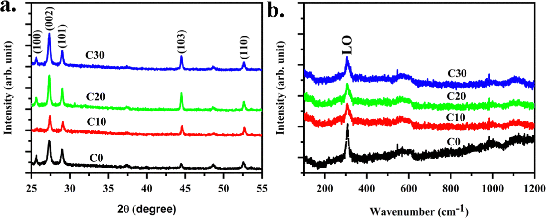
Structural properties of the Cu:CdS films on the glass substrates were examined through X-ray diffraction (XRD). The diffraction was recorded over the 2θ range from 25° to 55° (see Fig. 1a) (Fig. S1a for on FTO, ESI†). The recorded diffraction peaks agree with ICDD card no. 65-3414 conforming to the hexagonal phase.1 No peaks related to CdO or any other impurity phases were observed.21 An intense peak is recorded at 2θ = 27.33° in CdS films, suggesting the preferred growth orientation along the (002) plane. Cu2+ is a familiar transition element dopant with ionic radii of 0.096 nm, which is near to 0.097 nm of Cd2+.2 The diffraction peaks shifted towards higher 2θ values with the addition of Cu onto CdS, suggesting volume compression (Fig. S1b, ESI†). The mere change in the lattice parameter by this shift is due to the strain in the film, which is very small in the present scenario. The crystallite size for the samples is calculated using the intense diffraction peaks. From the Scherrer equation,22 the crystallite sizes corresponding to the (100), (002), and (101) planes were calculated and averaged out.| | D = 0.9λ/β![[thin space (1/6-em)]](https://www.rsc.org/images/entities/char_2009.gif) cosθ cosθ | (1) |
where D is crystallite size, and β is full width at half maximum. Calculated crystallite sizes are listed in Table 1. The ionic radius of Cu+ is 140 pm. The replacement of cadmium with higher volume copper atoms is expected to increase the growth in the same direction. Therefore, the crystallite size of Cu:CdS thin films is higher than that of pristine. There was a slight variation in the peak position and the crystallite size for the films deposited on FTO (Fig. S1b, ESI†) due to the crystallographic strain formed on the films. XRD of CuCdS/FTO films is given in Fig. S1a (ESI†), and the details are in the Table T1 (ESI†). Higher crystallite size in C10 (∼38 nm) compared to other compositions indicates lower residual strain, indicating that lower defect density could result in photo-sensitivity increment.
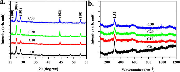 |
| | Fig. 1 (a) XRD and (b) Raman spectra for CuCdS thin films on glass substrates at different Cu concentrations. | |
Table 1 XRD parameters extracted for CuCdS thin films on glass substrates at different copper concentrations
| Sample |
Plane |
2θ (degree) |
FWHM (degree) |
Crystallite size (nm) |
Average D (nm) |
| C0 |
(100) |
25.64 |
0.21 |
40.2 |
29.8 |
| (002) |
27.33 |
0.39 |
21.9 |
|
| (101) |
28.99 |
0.31 |
27.2 |
|
|
|
| C10 |
(100) |
25.74 |
0.17 |
51.0 |
38.3 |
| (002) |
27.42 |
0.28 |
30.4 |
|
| (101) |
29.09 |
0.26 |
33.4 |
|
|
|
| C20 |
(100) |
25.64 |
0.22 |
38.9 |
35.1 |
| (002) |
27.33 |
0.28 |
30.3 |
|
| (101) |
29.00 |
0.24 |
36.0 |
|
|
|
| C30 |
(100) |
25.64 |
0.21 |
39.8 |
32.3 |
| (002) |
27.33 |
0.34 |
25.5 |
|
| (101) |
29.00 |
0.27 |
31.5 |
|
Investigation on the lattice vibrations in CuCdS thin films carried out using Raman spectroscopy. Fig. 1b displays Raman spectra of pristine and Cu-doped CdS thin films. Intense Raman lines detected in all samples confirm crystalline CuCdS thin films. All films exhibited a single peak close to 307 cm−1 corresponding to longitudinal optical phonon vibrations (LO).6 No additional peaks were observed indicating high purity phase CdS. Compared to CdS, a shift of 1 cm−1 in CuCdS, is assigned to surface optical phonon mode effects. The shift is due to the strain in films resulting from Cu incorporation creating lattice distortion or phonon momentum breakdown. The peak width of the Raman line increased from 11 cm−1 for CdS to nearly 23 cm−1 for Cu-doped CdS thin films as shown in the ESI† (Fig. S2), fitted using the Lorentzian function. The Raman line broadening is assigned to the incorporation of defects resulting in strain in the films. Using the full width at half maximum of the LO mode, the phonon lifetime is calculated.23
| | | Phonon lifetime, T = 1/2πcΓ | (2) |
where
Γ is the FWHM of the Raman line, and
c is the velocity of light. The calculated phonon lifetimes for CdS and CuCdS films were ∼45 ps and 22 ps, respectively. Hot phonon effects will play a role in carrier relaxation in CdS with a high phonon lifetime compared to CuCdS. The lower the phonon lifetime, the less heat generation in the fabricated photodetector is expected. Hence, Cu-doped CdS photodetectors are expected to live longer than CdS.
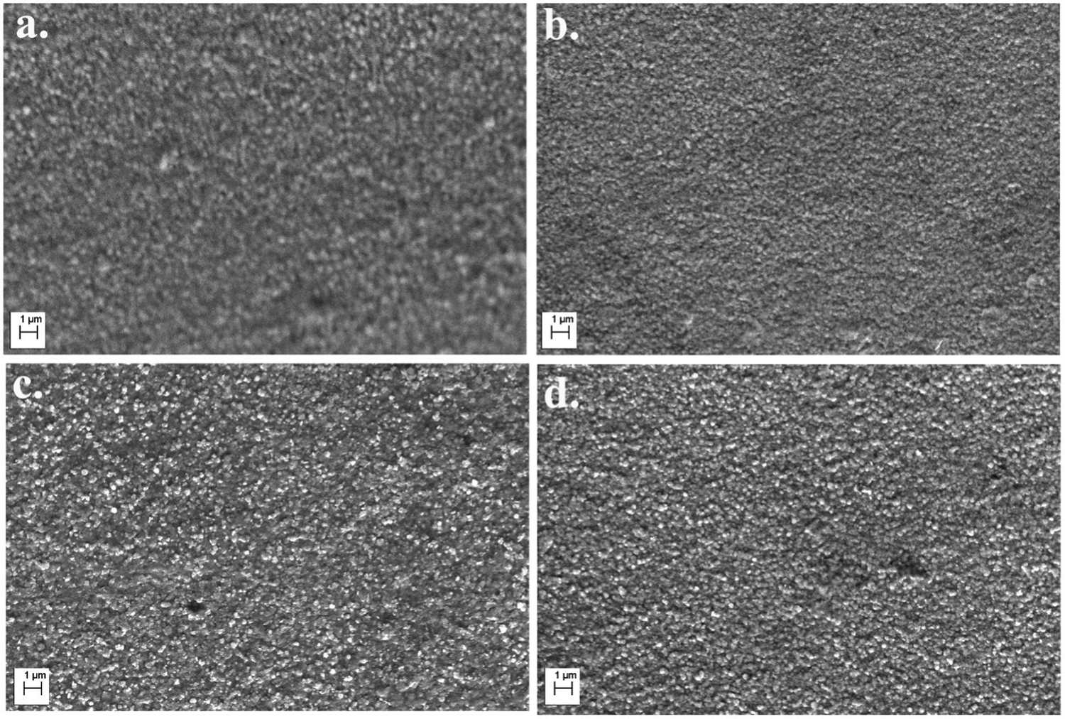
Fig. 2 demonstrates the surface morphologies of CdS and CuCdS thin films. All the films were pin hole-free, crack-free, homogeneous, and uniform. From EDX, the Cd/S ratio of undoped CdS thin films was greater than unity suggesting sulfur deficient non-stoichiometric films (Table 2). With the addition of Cu into CdS films, the Cd/S ratio decreases confirming the substitution of Cu ions into Cd lattices in the host.
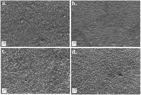 |
| | Fig. 2 Scanning electron micrographs of CuCdS thin films on glass substrates at different Cu concentrations: (a) 0 at% (b) 10 at% (c) 20 at% and (d) 30 at% of Cu. | |
Table 2 Elemental composition of CuCdS thin films on glass substrates obtained from EDX
| Sample |
Cd (at%) |
S (at%) |
Cd/S |
Cu (at%) |
Cu/(Cd + Cu) |
| CCS0 |
50.81 |
49.19 |
1.03 |
0.00 |
0.000 |
| CCS10 |
47.44 |
47.41 |
1.00 |
5.16 |
0.098 |
| CCS20 |
46.16 |
45.39 |
1.02 |
8.45 |
0.155 |
| CCS30 |
41.53 |
44.32 |
0.94 |
14.15 |
0.254 |
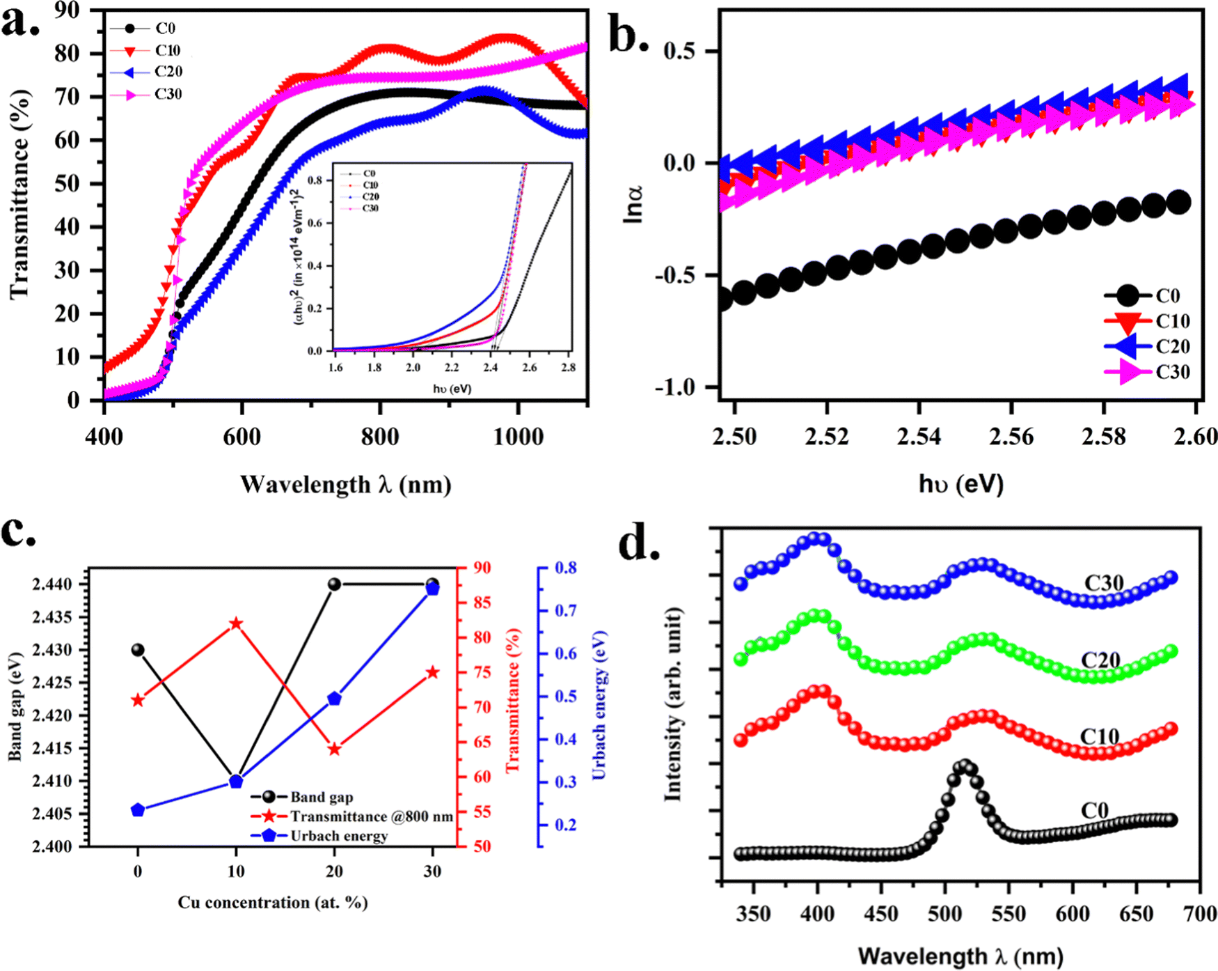
The optical properties of the CuCdS thin films were studied by employing a UV-Vis spectrophotometer and photoluminescence spectroscopy. The transmittance spectra of Cu:CdS thin films are shown in Fig. 3a. All the films had a transmittance of 60–80%, the maximum for the Cu10 sample. The transmittance of the CdS thin film increased with the addition of Cu. The transparent nature of the films indicates favourable optical properties of the deposited films. All the films show sharp transmittance drops at the fundamental absorption band edge (520 nm). The sharp band edge in the transmittance spectra confirms the good crystallinity of the CuCdS thin films. The band edge corresponds to electron excitation from the valence band to the conduction band and is related to the optical band gap.2 The energy band gap was estimated using the Tauc plot.24
where
α is the absorption coefficient,
A is the proportionality constant,
hϑ is the incident energy, and
Eg is the band gap of the material. For direct band gap material CdS,
n is ½. Inset of
Fig. 3a shows the plot of
hϑ vs. (
αhϑ)
2. Many authors have observed minor variation of the band gap with Cu doping on CdS.
2,14–16,18,25,26 Likewise, the band gap of the samples was almost the same for all compositions in the present study. However, there was a significant increment in the band tail as observed from the Tauc plot indicating an increased defect level upon doping. Therefore, using the relation between the absorption coefficient and photon energy near the band edge
27| | 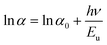 | (4) |
where
α0 is a constant, and
Eu is the width of the localized states known as the Urbach energy. The slope of ln
α vs. hν (
Fig. 3b) gives the Urbach energy. The variation in the band gap, transmittance, and Urbach energy with the copper dopant concentration is given in
Fig. 3c and
Table 3.
 |
| | Fig. 3 (a) Transmittance vs. wavelength (inset: Tauc plot), (b) Urbach plot, (c) variation of band gap, transmittance, and Urbach energy with Cu concentration in CuCdS and (d) photoluminescence spectra of CuCdS thin films on glass substrates at different Cu concentrations. | |
Table 3 Optical parameters obtained from a UV-Vis spectrophotometer for the CuCdS thin films
| Sample |
Transmittance at 800 nm (%) |
Band gap (eV) |
Urbach energy (eV) |
| C0 |
71 |
2.43 |
0.235 |
| C10 |
82 |
2.41 |
0.301 |
| C20 |
64 |
2.44 |
0.495 |
| C30 |
75 |
2.44 |
0.751 |
The lattice position of Cu atoms in the host CdS is detected using photoluminescence. Photoluminescence depends on the defect types in the material and their configuration. Emission spectra for the samples were recorded at an excitation wavelength of 325 nm (see Fig. 3d). The Cu atom in the CdS can either be substituted as a single acceptor state or interstitial to form a single donor state. The pristine CdS thin films had a single emission peak at 515 nm corresponding to the near band edge that matches with the band gap estimated from the Tauc plot. For copper doped CdS, along with near band edge emission, a defect related peak was observed at 560 nm. Upon Cu doping, the intensity of the near band edge emission quenched or decreased. Similar results have been reported in the past.25 Negligible shifts in the positions of the emission lines for different Cu-doped CdS thin films are observed (Fig. S3, ESI†).
The chemical state of the elements was investigated via X-ray photoelectron spectroscopy (Fig. S4a shows the survey spectra, ESI†). Fig. 4(a)–(c) shows the core spectra of Cu, Cd, and S on a glass substrate for sample C10. The peaks observed corresponding to the carbon (Fig. S4b, ESI†) and oxygen (Fig. S4c, ESI†) originate from impurities adsorbed during the measurement. Before the curve fitting, carbon correction was done at 284.8 eV. All the curve fittings were done using CASAXPS, with an error of ±0.1 eV. The error was reduced by using the Tougaard background function provided in the software. An oxygen peak with relatively negligible intensity was observed at binding energy 531.8 eV, which doesn’t belong to Cd–O or CdSO4.28 In the cadmium region, Cd 3d5/2 and Cd 3d3/2 characteristic peaks were observed at binding energies 405.24 eV and 411.98 eV. The difference between the B.E. of Cd 3d5/2 and 3/2 electrons is about 6.74 eV proving the existence of Cd in the +2 oxidation state.15,29 For standard CdS, Cd 3d5/2 occurs at 405 eV of B.E.28 Therefore, a shift in this peak towards higher B.E. is in line with the Cd/S ratio from EDX being nearly 1 for C10, indicating a decent defect density.28 Such a low level of defect density (compared with ref. 28) can produce a faster response. Peaks observed at 162.73 eV and 161.54 eV were assigned to S2p1/2 and 2p3/2 of the C10 sample.29 Similarly, the Cu 2p spectrum (Fig. 4a) reveals two peaks at the binding energies 949.33 eV and 929.53 eV corresponding to Cu2p 1/2 and Cu2p 3/2 electrons. Here, the difference between the two peaks is 19.8 eV, which corresponds to the +1 oxidation state of Cu.13 In addition, there are no satellite peaks in between the Cu2p3/2 and ½ peaks. No peaks corresponding to the Cu(II) are observed. The +1 oxidation state of Cu provides a greater hole carrier concentration, giving rise to p-type CdS. The fitting parameters are provided in Table T2 in the ESI.†
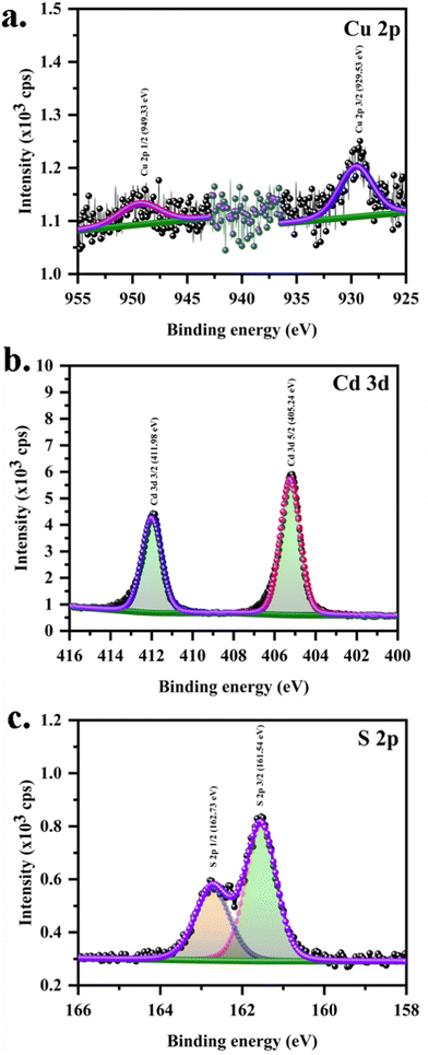 |
| | Fig. 4 XPS peak fit for core level spectra of (a) Cu 2p, (b) Cd 3d and (c) S 2p for CuCdS thin films on glass substrates at Cu = 10 at% in CuCdS. | |
Electrical parameters such as carrier concentration, mobility, and resistivity were measured by employing the van der Pauw method. The measurements were carried out for the 0.5 cm2 samples using a 1.5 T magnetic field and 1 nA current, and a four-probe sample holder interfaced with a Keithley 2450. The obtained values are given in Table 4. For pristine CdS, a negative hall coefficient was observed indicating n-type carriers whereas Cu-doped CdS thin films were p-type. The high carrier concentration of p-type carriers in Cu-doped CdS films is owing to the Cu 3d level. Cu acting as acceptor centres in CdS results in p-type conductivity. High carrier concentration resulted in low mobility of holes in Cu:CdS. However, with the increment in the copper concentration in CdS, the conductivity improved.
Table 4 Electrical properties of CuCdS thin films on glass substrates using the van der Pauw technique
| Sample |
Carrier concentration (cm3) |
Resistivity (Ohm cm) |
Mobility (cm2 V−1 s−1) |
Carrier type |
| C0 |
2.7 × 10¹² |
24 |
9.73 |
n |
| C10 |
1.04 × 10¹³ |
42 |
1.44 |
p |
| C20 |
1.4 × 10¹³ |
29 |
1.56 |
p |
| C30 |
8.8 × 10¹³ |
798 |
1.50 |
p |
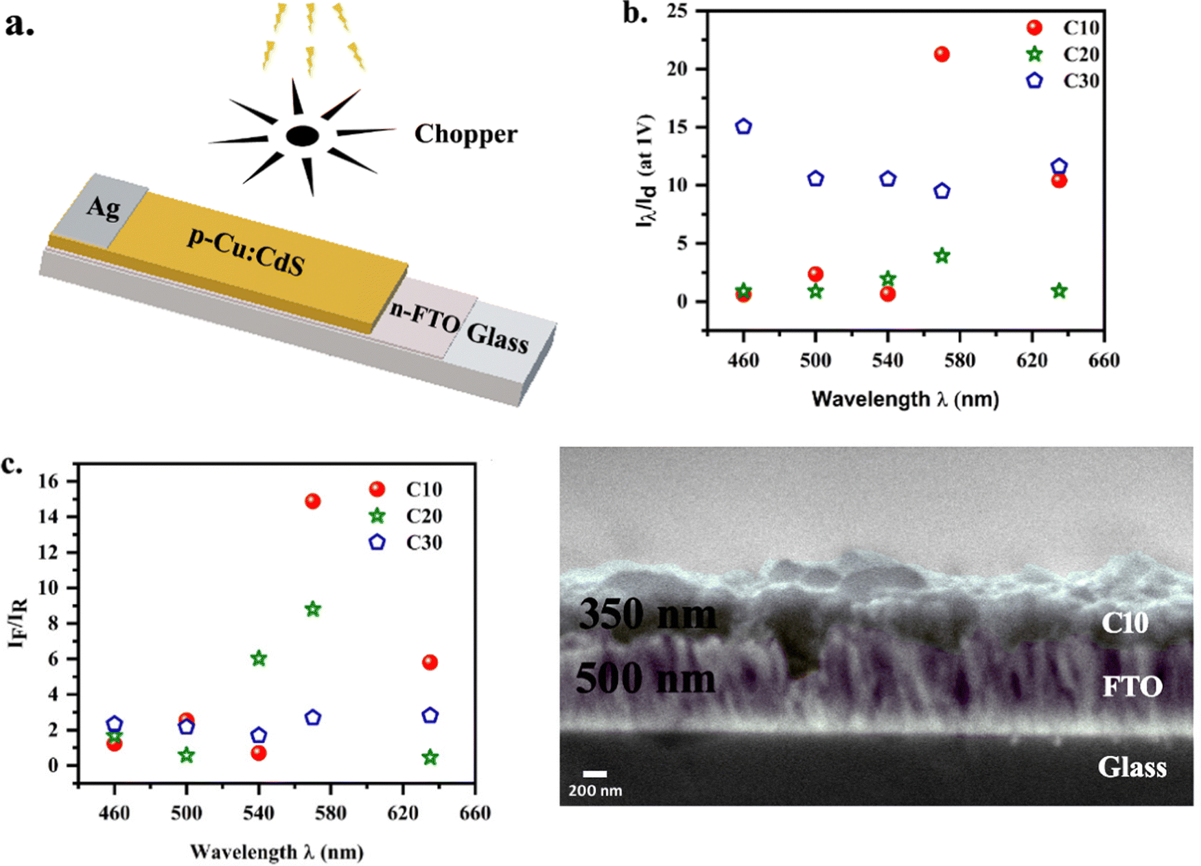
To investigate the effect of copper doping on photoconduction, I–V characteristics for all thin films in the device configuration shown in Fig. 5a are recorded. The ratio of photocurrent to dark current for all samples is shown in Fig. 5b. The dark current increased with the increase in Cu concentration. Iph was maximum for the C10/FTO sample. The rectification ratio viz., If/Ir, and the photocurrent to dark current were higher for the C10/FTO sample at 1 V (Fig. 5c). Therefore, photo-detection and response studies were performed in detail for this sample. The I–V curves for other samples can be found in the ESI† (Fig. S5a and b). Fig. 5d displays the SEM cross sectional image at a magnification of 30k × for C10/FTO with the thickness of 350 nm/500 nm.
 |
| | Fig. 5 (a) Schematic of the photodetector fabricated, variation of the ratio of (b) photocurrent/dark current and (c) forward current/reverse current (rectification ratio) at various wavelengths for C10/FTO, C20/FTO and C30/FTO samples, and SEM cross-sectional image of C10/FTO. | |
The variation of the current was measured in the dark and under illumination in the range of −1 V to +1 V for C10/FTO. For the measurement of the photoelectrical properties, light of different wavelengths such as 460 nm (indigo, 50 μW cm−2), 500 nm (blue, 250 μW cm−2), 540 nm (green, 400 μW cm−2), 570 nm (yellow, 450 μW cm−2) and 635 nm (red, 450 μW cm−2) is made to incident vertically on the p-CdS/n-FTO heterojunction and the corresponding photoelectric behavior is recorded. The photocurrent was measured under band-to-band optical excitation. Under this condition, the photogenerated electrons increase the concentration of charge carriers in the CB, increasing the photoconductivity.
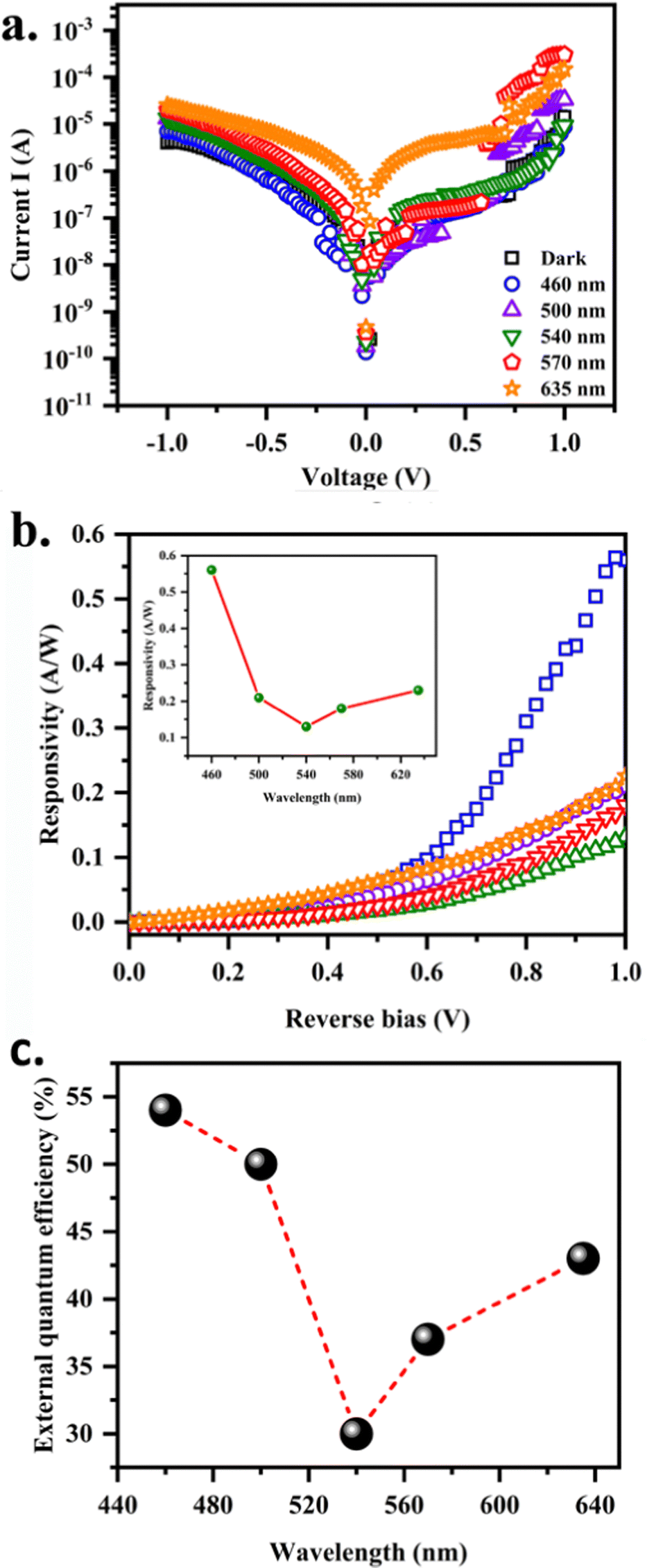
Fig. 6a displays the current–voltage curves of photodetectors illuminated with different wavelengths and under dark conditions. The dark current increased with the increase in bias voltage. Only a small dark current is measured with the applied voltage due to high photoconductor resistance. The generation of charge carriers will enhance under illumination and as a result a very high photocurrent flows. The dark current is of the order of 10−7 A, whereas the photocurrent was of the order of 10−5 A at 0.7 V bias. It is seen that with the increase in applied voltage, the photocurrent in CuCdS PDs significantly increased in both dark and illumination sections. CuCdS exhibits a maximum net current of the order of 102. This increment in current is due to the stimulated electrons from VB into CB under illumination wherein the creation of pairs of free holes and electrons at the VB and CB occurs. Photocurrent went on increasing from longer wavelength to shorter and was maximum at 460 nm. Significant improvement in the photocurrent was observed when the device was illuminated with shorter visible wavelengths. Thus, the photodetectors are highly sensitive to visible light. The ray of photons with energy >2.4 eV, viz., higher than the band gap of CuCdS produced more hole–electron pairs. Thus, the optimum wavelength equal to or greater than the band gap (λinc < 520 nm) showed higher photocurrent.
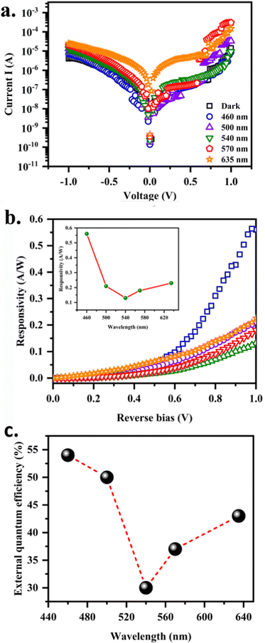 |
| | Fig. 6 (a) I–V characteristics recorded in C10/FTO at various incident wavelengths, (b) responsivity in the reverse bias (inset: corresponding variation of responsivity with wavelength) and (c) variation in EQE with wavelength for the C10/FTO photodetector. | |
The responsivity of the detector is defined as the photocurrent generated per unit power of the incident light on the effective area.11
| |  | (5) |
where
Iph is photocurrent (in A),
P is power incident on the device (mW cm
−2) and
A is the area of the device (in cm
2). In measuring the photoelectrical properties in the reverse bias, light with different wavelengths vertically incident on the PD and photoresponsivity is calculated. Note that responsivity varies with wavelength, which could be understood from calculating the quantum efficiency (EQE). The influence of the wavelength on the photoresponse is shown in
Fig. 6b, derived using
Fig. 6a. The photocurrent increases when the wavelength of light decreases from 635 nm to 460 nm. The shorter excitation wavelength provides higher excitation energy increasing the photocurrent like the case of forward bias.
EQE is the number of electron–hole pairs excited per photon, and is a critical parameter for a photodetector.11
| |  | (6) |
where
h,
c, and
q are Planck's constant, the velocity of light under vacuum, and electron charge.
λ is the incident photon wavelength. The EQE at a forward bias voltage of 1 V is given in
Fig. 6c. A maximum quantum efficiency of more than 50% is observed for 460 nm light. Similarly, the figure of merit of a photodetector is the linear dynamic range (LDR). With photocurrent and dark current densities of
Jph and
Jdark, LDR is given by:
30| |  | (7) |
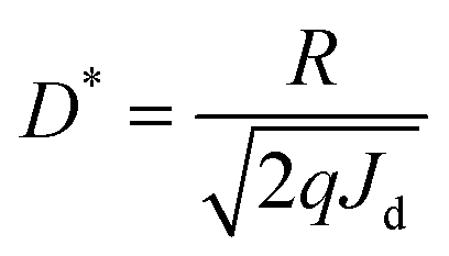
Detectivity,
D* at a particular bias with current density
Jd is given by:
11| |  | (8) |
The maximum LDR of around 43 dB was observed at a bias of 0.7 V. The detectivity at 1 V for 570 nm light wavelength was 6.3 × 10
11 Jones.
Response and recovery times signify the sensitivities and performance of PDs in real-world applications. The slow response of the photodetector limits the practical applications. Based on the device structure, the response time for rise and fall differs. The photosensitivity response of the PDs was obtained at 1 V of constant bias for ON/OFF cycles from the optical chopper placed in front of a Xe lamp, which helps for pulsing the light at the frequency 1 Hz. Fig. 7 shows the time response of photocurrent in the photodetector under visible light. The rise time is defined as the time required to increase the photocurrent up to 63% (1 − (1/e)) from the dark current, and the decay time is the time required to drop the maximum photocurrent to 37% (1/e). The rise times were 33 ms, 11 ms and, 59 ms at 460 nm, 500 nm and, 540 nm of illumination. The decay times for the same set of wavelengths were 170 ms, 21 ms, and 78 ms. The shape of the response curve could be explained as follows. The initial increase in the photocurrent upon illumination is due to the photocarrier generation. The slowly increasing component of the photocurrent, while the light is still on, is due to the photo enhanced mobility. This depends on the photogenerated holes getting trapped at the grain boundaries, filling of carriers into the trapping centres in the bulk, and recombination of the carriers at the surface and in the bulk. The presence of surface state and sulfur vacancies (Fig. 8a) adsorbed oxygen through the chemo/physio adsorption process (Fig. 8b). Adsorbed oxygen extracts electrons from the conduction band of CdS. The electron density reduces the dark current.
| | | O2(g) + e− → O2−(ads) | (R4) |
Under illumination, electron–hole pairs formed in CdS. Photogenerated holes release trapped electrons in oxygen (
Fig. 8c), which flow through the film creating current.
28| | | O2−(ads) + h+ → O2(g) | (R5) |
As the light turns off, slow mobility of charges will slowly decrease the photocurrent. The sample with higher Cu concentrations will have higher grain boundaries which will quench the photocurrent during illumination.
14 The Cu dopant that acts as an acceptor supports the recombination of holes at the grain boundaries. After illumination is off, the photocurrent goes down slowly, due to the lower recombination of charge carriers at the grain boundaries. The switching between the on/off states was very fast and reversible, permitting the device to perform as a high-quality photosensitive switch. The current levels for on and off remain almost constant for more than 40 cycles indicating reproducibility and stability of the device. Furthermore, on/off switching was observed for the on/off light frequency of 20 Hz at each wavelength. The crucial parameters of the photodetector prototype prepared in the present work,
viz., Cu:CdS/FTO compared with various other photodetectors reported
3,11,21,31–38 are shown in
Fig. 9. Mohd. Shkir
et al. have reported a responsivity of 0.213 A W
−1 for CdS thin films at 532 nm and a power of 0.316 mW cm
−2.
11 The same group has reported a responsivity of 0.0141 A W
−1 for CdS thin films.
36 Husham
et al. fabricated self-powered CdS photodetectors with a responsivity of 0.24 A W
−1 at 500 nm.
4 Waldiya
et al. have reported responsivity between 0.0715 and 0.3815 A W
−1.
5 Dharani Devi
et al. have reported a responsivity between 0.15 and 0.24 A W
−1 for CdS thin films.
3 The comparison table can be found in the ESI
† (Table T3). The responsivity of CdS in this study is lower compared to other reports, which could be due to the difference in the incident wavelength of the source.
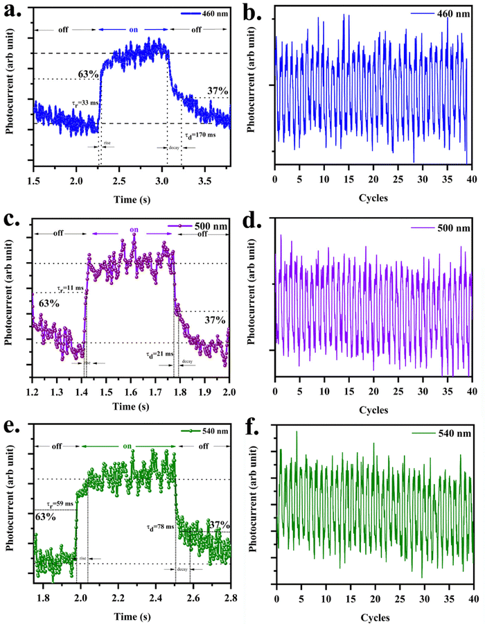 |
| | Fig. 7 (a), (c) and (e) Photoresponse curve for different incident wavelengths on C10/FTO, and (b), (d) and (f) figure showing the stability of photocurrent and on/off ratio over 40 cycles. | |
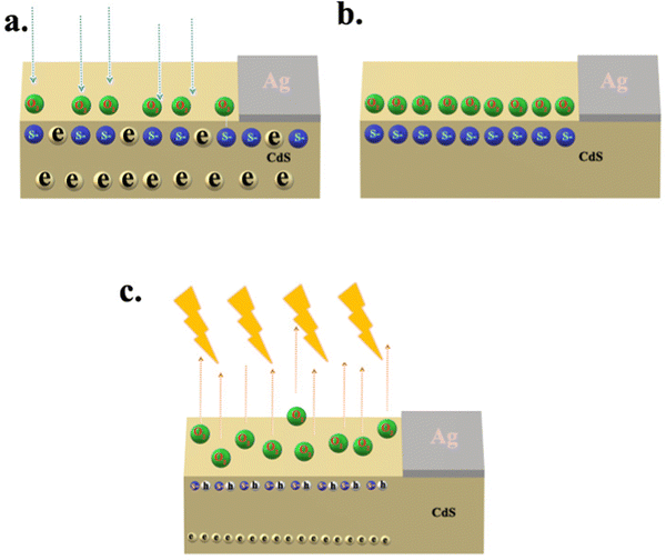 |
| | Fig. 8 Schematics of the oxygen adsorption (under dark – a and b) and desorption (under illumination – c) on surface defects of CdS thin film. | |
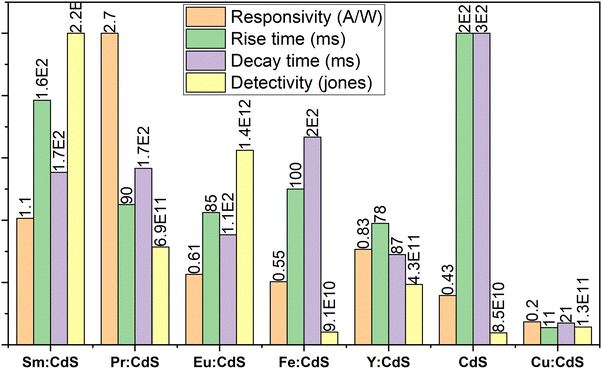 |
| | Fig. 9 Comparison of the present work (Cu:CdS) with other doped CdS photodetectors and their photodetection capabilities. | |
Conclusion
A low cost, industrially beneficial CuCdS photodetector is fabricated that works in the visible wavelength regime of the solar spectrum, with a band gap of 2.4 eV. The best device exhibited responsivity of 0.2 A W−1, with EQE of 50 to 53.9% under light of wavelengths 500 nm and 460 nm illumination. The rise and fall times were recorded as 11 ms and 21 ms respectively, and were better than most of the reported works. Using a simple device structure, an excellent responsivity, speed, and stability were observed for a copper concentration of 10 at% in CdS. Copper in the +1 state was confirmed from X-ray photoelectron spectroscopy, which was responsible for the p-type conductivity in CdS as observed from the Hall effect. The highest crystallinity observed for the C10 sample supports the mechanism of better photodetection compared to other compositions. Moreover, all the samples had high transmittance, and henceforth could be further used in flexible transparent photodetection applications.
Conflicts of interest
There are no conflicts to declare.
Acknowledgements
Ganesha Krishna V S is thankful to the Department of Science and Technology, India – DST INSPIRE-Innovation in Science Pursuit for Inspired Research fellowship (IF190268) for funding aid, BITS PILANI Goa for extending Raman and PL characterization, IIT Roorkee for extending XPS characterization, and IISc CeNSE for extending XRD.
References
- Y. Su,
et al., Dense CdS thin films on fluorine-doped tin oxide coated glass by high-rate microreactor-assisted solution deposition, Thin Solid Films, 2013, 532, 16–21, DOI:10.1016/j.tsf.2012.12.040.
- M. Shaban, M. Mustafa and A. M. El Sayed, Structural, optical, and photocatalytic properties of the spray deposited nanoporous CdS thin films; influence of copper doping, annealing, and deposition parameters, Mater. Sci. Semicond. Process., 2016, 56, 329–343, DOI:10.1016/j.mssp.2016.09.006.
- M. D. Devi, A. V. Juliet, K. H. Prasad, T. A. A. M. Alshehri and M. Shkir, An effect of precursor concentrations on the photodetection capabilities of CdS thin films for high – efficiency visible – light photodetector applications, Appl. Phys. A: Mater. Sci. Process., 2020, 126(12), 1–11, DOI:10.1007/s00339-020-04067-3.
- M. Husham, Z. Hassan and A. M. Selman, Synthesis and characterization of nanocrystalline CdS thin films for highly photosensitive self-powered photodetector, Eur. Phys. J. Appl. Phys., 2016, 74, 1–8, DOI:10.1051/epjap/2016150414.
- M. Waldiya, R. Narasimman, D. Bhagat, D. Vankhade and I. Mukhopadhyay, Nanoparticulate CdS 2D array by chemical bath deposition: characterization and optoelectronic study, Mater. Chem. Phys., 2019, 226, 26–33 CrossRef CAS.
- S. N. Moger and M. G. Mahesha, Investigation on spectroscopic and electrical properties of p-Si/CdSxSe1−x (0 ≤ x ≤ 1) heterostructures for photodetector applications, J. Alloys Compd., 2021, 870, 159479, DOI:10.1016/j.jallcom.2021.159479.
- S. N. Moger, P. Kumar, G. K. Rao and M. G. Mahesha, Annealing assisted enhancement in photo response of PV deposited CdS thin films, Opt. Laser Technol., 2022, 149, 107868, DOI:10.1016/j.optlastec.2022.107868.
- I. S. Yahia, I. M. El Radaf and A. M. Salem, Chemically deposited Ni-doped CdS nanostructured thin films: Optical analysis and current-voltage characteristics, J. Alloys Compd., 2019, 776, 1056–1062 CrossRef CAS.
- N. H. Patel, M. P. Deshpande, S. V. Bhatt and S. H. Chaki, Structural and magnetic properties of undoped and Mn doped CdS nanoparticles prepared by chemical co-precipitaion method, Adv. Mater. Lett., 2014, 5, 671–677 CrossRef CAS.
- S. R. Ferra-Gonzalez,
et al., Optical and structural properties of CdS thin films grown by chemical bath deposition doped with Ag by ion exchange, Optik, 2014, 125, 1533–1536 CrossRef CAS.
- M. Shkir, I. M. Ashraf, A. Khan, M. Taukeer, A. M. El-toni and S. Alfaify, Sensors and Actuators A: Physical A facile spray pyrolysis fabrication of Sm: CdS thin films for high-performance photodetector applications, Sens. Actuators, A, 2020, 306, 111952, DOI:10.1016/j.sna.2020.111952.
- P. Chand and R. Ghosh, Investigation of structural, morphological and optical properties of Zn doped CdS nanostructures synthesized via co-precipitaion method, Optik, 2018, 161, 44–53 CrossRef CAS.
- M. Panthakkal, A. Muthalif, Y. Lee, C. Damodharan, H. Kim and Y. Choe, Applied Surface Science Enhanced photovoltaic performance of quantum dot-sensitized solar cells with a progressive reduction of recombination using Cu-doped CdS quantum dots, Appl. Surf. Sci., 2017, 396, 582–589, DOI:10.1016/j.apsusc.2016.10.200.
- R. Panda, V. Rathore, M. Rathore, V. Shelke and N. Badera, Applied Surface Science Carrier recombination in Cu doped CdS thin films: photocurrent and optical studies, Appl. Surf. Sci., 2012, 258, 5086–5093, DOI:10.1016/j.apsusc.2012.01.131.
- S. Wang,
et al., Materials Science in Semiconductor Processing Influence of Cu doping on physical and photo-electrochemical properties of CdS thin films prepared by RF magnetron sputtering, Mater. Sci. Semicond. Process., 2021, 133, 105933, DOI:10.1016/j.mssp.2021.105933.
- P. J. Sebastian, p - type CdS thin films formed by in situ Cu doping in the chemical bath p-type CdS thin films formed by in sifu Cu doping in the chemical bath, Appl. Phys. Lett., 1993, 62, 2956–2958, DOI:10.1063/1.109181.
- Z. R. Khan, M. Shkir, V. Ganesh and S. Alfaify, Linear and Nonlinear Optics of CBD Grown Nanocrystalline F Doped CdS Thin Films for Optoelectronic Applications: An Effect of Thickness Growth of Films, J. Electron. Mater., 2018, 47(9), 5386–5395, DOI:10.1007/s11664-018-6437-9.
- B. Sharma, A comprehensive study of structural, optical and electrical properties of Cu doped CdS nanocrystalline thin films: for optoelectronic applications, J. Mater. Sci.: Mater. Electron., 2022, 33(14), 11601–11612, DOI:10.1007/s10854-022-08132-w.
- A. Izgorodin, O. Winther-jensen, B. Winther-jensen and D. R. Macfarlane, CdS thin-film electrodeposition from a phosphonium ionic liquid, Phys. Chem. Chem. Phys., 2009, 8532–8537, 10.1039/b906995j.
- S. Chander and M. S. Dhaka, Optimization of substrates and physical properties of CdS thin films for perovskite solar cell applications, J. Mater. Sci.: Mater. Electron., 2017, 28, 6852–6859, DOI:10.1007/s10854-017-6384-x.
- J. Zhang,
et al., Research on FTO/CBD – CdS: Cl thin film photodetector with a vertical structure, Appl. Phys. A: Mater. Sci. Process., 2021, 1–8, DOI:10.1007/s00339-021-04704-5.
- P. Scherrer, Bestimmung der inneren Struktur und der Gro ße von Kolloidteilchen mittels Rontgenstrahlen, Kolloidchem. Ein Lehrb., 1912, 387–409 Search PubMed.
- M. Millot, R. Tena-Zaera, V. Munoz-Sanjose, J. Broto and J. Gonzalez, Anharmonic effects in ZnO optical phonons probed by Raman spectroscopy, Appl. Phys. Lett., 2010, 96(15), 152103, DOI:10.1063/1.3387843.
- J. Tauc, and Menth, States in the gap, J. Non-Cryst. Solids, 1972, 8(10), 569–585 CrossRef.
- M. Muthusamy and S. Muthukumaran, Optik Effect of Cu-doping on structural, optical and photoluminescence properties of CdS thin films, Opt. - Int. J. Light Electron Opt., 2015, 126(24), 5200–5206, DOI:10.1016/j.ijleo.2015.09.186.
- R. Lo and R. Rangel, Electrical characterization of Cu-doped CdS p-type thin film transistors, J. Mater. Sci.: Mater. Electron., 2021, 32, 25462–25472, DOI:10.1007/s10854-021-07006-x.
- F. Urbach, The Long-Wavelength Edge of Photographic Sensitivity and of the Electronic Absorytion of Solids, Phys. Rev., 1953, 92(5), 1324 CrossRef CAS.
- D. I. Halge,
et al., Development of highly sensitive and ultra – fast visible – light photodetector using nano – CdS thin film, Appl. Phys. A: Mater. Sci. Process., 2021, 127(6), 1–11, DOI:10.1007/s00339-021-04611-9.
- T. Abe, Y. Kashiwaba, M. Baba, J. Imai and H. Sasaki, XPS analysis of p-type Cu-doped CdS thin films, Appl. Surf. Sci., 2001, 176, 549–554 CrossRef.
- B. Hanna and K. P. Surendran, Low temperature-processed ZnO thin films for p–n junction-based visible-blind ultraviolet photodetectors, RSC Adv., 2018, 37365–37374, 10.1039/c8ra07312k.
- M. Shkir, I. M. Ashraf, S. Alfaify, A. M. El-toni, M. Ahmed and A. Khan, A noticeable effect of Pr doping on key optoelectrical properties of CdS thin films prepared using spray pyrolysis technique for high-performance photodetector applications, Ceram. Int., 2020, 46(4), 4652–4663, DOI:10.1016/j.ceramint.2019.10.196.
- M. Shkir,
et al., A significant enhancement in visible-light photodetection properties of chemical spray pyrolysis fabricated CdS thin films by novel Eu doping concentrations, Sens. Actuators, A, 2019, 301, 111749 CrossRef.
- L. Li,
et al., Single-crystalline CdS nanobelts for excellent field-emitters and ultrahigh quantum-efficiency photodetectors, Adv. Mater., 2010, 22(29), 3161–3165 CrossRef CAS PubMed.
- M. Shkir,
et al., Facile fabrication of Ag/Y: CdS/Ag thin films-based photodetectors with enhanced photodetection performance, Sens. Actuators, A, 2021, 331, 112890, DOI:10.1016/j.sna.2021.112890.
- Y. Pei,
et al., CdS-Nanowires Flexible Photodetector with Ag-Nanowires Electrode Based on Non-transfer Process, Nat. Publ. Gr., 2016, 6, 1–10, DOI:10.1038/srep21551.
- M. Shkir and T. Alshahrani, The physical properties of CdS thin films through incorporation of Fe dopant for photodetector applications, J. Phys. Chem. Solids, 2023, 177(2022), 111282, DOI:10.1016/j.jpcs.2023.111282.
- B. Jin,
et al., Self-Limited Epitaxial Growth of Ultrathin Nonlayered CdS Flakes for High-Performance Photodetectors, Adv. Funct. Mater., 2018, 28(20), 1–9, DOI:10.1002/adfm.201800181.
- K. Deva Arun Kumar, Paolo Mele, M. Anitha and S. Varadharajaperumal, Simplified chemical processed Cd1−xAlxS thin films for high-performance photodetector applications, J. Phys.: Condens. Matter, 2021, 33(19), 195901, DOI:10.1088/1361-648X/abf199.
|
| This journal is © The Royal Society of Chemistry 2024 |
Click here to see how this site uses Cookies. View our privacy policy here. 
 Open Access Article
 This Open Access Article is licensed under a Creative Commons Attribution-Non Commercial 3.0 Unported Licence
 *
*