 Open Access Article
Property enhancement of a close-spaced sublimated CdTe thin film by a post-growth activation step with CdCl2 and MgCl2
Afrina
Sharmin
 ,
Syed Shafquat
Mahmood
,
Munira
Sultana
,
Md Aftab Ali
Shaikh
and
Muhammad Shahriar
Bashar
,
Syed Shafquat
Mahmood
,
Munira
Sultana
,
Md Aftab Ali
Shaikh
and
Muhammad Shahriar
Bashar
 *
*
Bangladesh Council of Scientific and Industrial Research (BCSIR), Bangladesh. E-mail: bashar@bcsir.gov.bd
First published on 14th December 2023
Abstract
The deposition parameters utilized during cadmium telluride (CdTe) film formation can regulate the microstructure of the absorber layer, which is crucial to photovoltaic conversion. In this study, borosilicate glass substrates are coated with CdTe thin films using the close-spaced sublimation approach under various argon pressures. At low pressure, a relative increase in grain size could be seen. A non-toxic magnesium chloride (MgCl2)-based activation procedure of the CdTe thin film absorber layer has been followed and contrasted with the conventional cadmium chloride (CdCl2) for solar cell applications. X-ray diffraction (XRD), Raman spectroscopy, scanning electron microscopy (SEM), electron dispersive spectroscopy (EDS), and ultraviolet-visible spectroscopy (UV-Vis) analyses of the impacts of the CdCl2 and MgCl2 activation treatment revealed the crystallization, morphology, composition, and optical attributes of the CdTe thin film. The Raman peak at 141 cm−1 is accredited to a mixture of CdTe's transversal optic phonons after chloride treatment. The main diffraction peaks, corresponding to the (111), (220), and (311) cubic plane according to JCPDS card number 96-900-8841, appear prominently at 2θ = 23.8°, 39.29° and 46.91°, respectively. The SEM image reveals that crystals in the MgCl2-treated CdTe thin film are quite highly textured. In addition, the treated CdTe samples show less absorbance than CdTe where the band gap varies between 1.48 and 1.56 eV and the refractive index ranges from 2.8–2.9, and the treatment effect is not that prominent. However, based on other structural and optical factors, it is evident that MgCl2 is the ideal activator for industrial purposes because it is eco-friendly, non-toxic, affordable, and provides comparable efficiency to conventional toxic CdCl2 activators.
1. Introduction
For explicit energy applications, integrated photovoltaics in buildings, unmanned vehicles, or in space, thin-film devices are extremely attractive.1 Cadmium telluride has been entrenched as the premier thin-film photovoltaic technology. It is a simple binary compound and is a direct band gap semiconductor material. Near stoichiometric CdTe which is the most stable phase is easy to fabricate and dissolves evenly. Additionally, CdTe can be synthesized using a variety of techniques.2 The development of CdTe technology aims to reduce energy production costs while also minimizing the ecological impact of indirect pollution. The pricing of CdTe solar cells has now fallen below $0.46 per Watt, pushing power generation costs closer to grid parity.3,4Based on the material's configuration and exterior dopants introduced, CdTe will be present in p-type, i-type, or n-type conduction methods.5 Tellurium-rich CdTe layers behave as n-type materials, whereas cadmium-rich CdTe layers do the opposite. Reliant on the original electrical conduction type of the precursor material, the accumulation of an n-type dopant (Cl) to CdTe may provide a wide range of effects. Owing to self-compensation from inherent imperfections such as vacancies (VCd, VTe), interstitial defects, or grain boundaries,6,7 CdTe has the disadvantage of it being difficult to attain large doping concentrations. Thus, these are the major hurdles in improving the power conversion efficiency of CdTe solar cells. For high conversion efficiency, the post-growth activation stage is an essential aspect of the CdTe solar cell design process. This is necessary for attaining high device efficiencies because it forms the photovoltaic junction at the CdTe/CdS interface8 to promote the growth of grains and recrystallization9 for passivation of the grain boundaries.10 This step also facilitates the p-type doping of the CdTe absorber layer.11 A variety of methods for cadmium chloride (CdCl2) deposition have been used, including methanolic solution and direct vapor exposure. Preceding annealing in an air or oxygen environment,12 the far more popular method is to apply a thin CdCl213,14 coating to the back surface via thermal evaporation. CdCl2 is common in CdTe device activation,15 with a few significant outliers, like handling in the presence of freon gas, as Romeo et al. observed.16 However, CdCl2 has two significant drawbacks. First, it is expensive (∼30 cents per g). Secondly, water-soluble Cd2+ is a potentially mobile source of hazardous elements posing a risk to personnel and the environment as well.17 However, the most expensive part of CdCl2 production is its processing and waste disposal, which necessitates a specialized industrial plant for the operator's safety. As a result, it's appealing to look into nontoxic and low-cost alternative chloride sources for post-growth treatment of CdTe absorber thin films as remarkably, there seems to be little existing research in this domain.
Cadmium chloride has been used for over 30 years18 and there have been relatively few efforts to utilize alternatives; for example, doping of Au or Cu,19 HCl,20 NaCl and KCl21 and NH4Cl22,23 treatments have been reported but with little success. In this study, a post-activation solution treatment using MgCl2 along with CdCl2 is illustrated which previously showed efficiencies (∼13%) for vapor treatment identical to those of a CdCl2-treated group.21 Consequently, it is nontoxic and costs less than a cent per g. It possesses comparable hole densities in the active layer (9 × 1014 cm−3) along with contamination profiles for Cl and O, which are key p-type dopants in CdTe thin films.21 CuCl2 and ZnCl2, for example, were not considered because they pose an environmental danger or have a high cost. One significant finding is that polycrystalline CdTe cells are considerably superior to single-crystal cells when followed by Cl2 heat treatment. Then, the grain boundaries actively aid the carrier collecting efficiency rather than serving as recombination hotspots.24 This suggests that the key to producing high-efficiency solar cells is the accumulation of Cl2 at the grain boundaries by Cl2 treatment. In our previous work, there is a correlation between the structural and optoelectronic properties of CdTe thin films with the variation of the Argon pressure.25 This correlation indicates significant commercial certainty. We have used the same samples to study the post-growth treatment with two selective chlorides for this study. The effect of MgCl2 and CdCl2 treatment on the properties of CdTe thin films is optimized and compared in this communication for solar-cell applications as a consequence of as-deposited CdTe1,26 which will contribute towards the understanding of this activation step. MgCl2 has potential as a non-carcinogenic low-cost alternative to CdCl2 without sacrificing device performance or requiring major changes in processing techniques. Our findings show that CdCl2 can be swapped immediately with MgCl227 in the conventional manufacturing process, reducing both the costs and environmental risk of CdTe photovoltaic module utilization. However, there is still a lot of room for exploration.
2. Experimental
2.1. Thin film deposition
The CdTe thin film is grown on borosilicate glass (BSG) by a close-spaced sublimation (CSS) method under ambient argon (Ar) with the source temperature and substrate temperature as 625 °C and 585 °C, respectively. The source and substrate are separated by 2 mm and the deposition pressure of the CSS chamber is varied from 250–1000 mTorr to identify the suitable deposition ambient for the CdTe thin film. The deposition process is continued for 10 min to fabricate a CdTe thin film. After that the unit is left for a while for self-cooling and the sample is collected later. The whole procedure is vividly described in a previous study.252.2. Chloride treatment
The CdTe thin film is etched with CdCl2 and MgCl2 for 3 s preceding to post-growth heat treatment to boost the Cl in-diffusion into the CdTe thin film. The samples are then desiccated with N2 flow. The heat treatment periods for the MgCl2 and CdCl2 treatments are 15 min at 390 °C with a ramp of 10 °C min−1. The samples are annealed in an air tube furnace with N2 flow maintained at 40 sccm. After self-cooling, the CdTe thin film is collected for characterization. The conditions of different deposition and post-growth activation steps are listed in Table 1. As the soda lime glass (SLG) substrate contains about 4% MgO,21 to exclude the effect of Mg, BSG is used as a regular substrate for this study.| Sample | Source temp. | Substrate temp. | Source-substrate spacing | Deposition time | Deposition pressure (Ar) | Treated with |
|---|---|---|---|---|---|---|
| P 250 Cd | 625 °C | 585 °C | 2 mm | 10 min | 250 mTorr | CdCl2 |
| P 500 Cd | 500 mTorr | |||||
| P 750 Cd | 750 mTorr | |||||
| P 1000 Cd | 1000 mTorr | |||||
| P 250 Mg | 250 mTorr | MgCl2 | ||||
| P 500 Mg | 500 mTorr | |||||
| P 750 Mg | 750 mTorr | |||||
| P 1000 Mg | 1000 mTorr |
2.3. Characterization
All treated CdTe absorber thin films were subjected to X-ray diffraction (XRD) to determine the microstructure of the film. Cu-K radiation with a wavelength of 1.5406 is used in a GBC, EMMA (Australia) diffractometer to record XRD patterns. Raman spectroscopy (LabRAM HR Evolution, Horiba Scientific, Japan) is used to obtain the compounds’ unique structural fingerprints. To investigate the optical absorbance at the visible wavelength, a UV-visible spectrophotometer (UH4150, Hitachi) is used. Film morphology is observed with a scanning electron microscope (SEM, EVO18, Zeiss). Energy-dispersive X-ray spectroscopy (EDX) was utilized to examine the chemical configuration of the film, using an EDS system (EDAX, AMETEK, USA) mounted to the scanning electron microscope. The beam voltage is maintained at 15 kV.3. Results and discussion
3.1. Structural characterization
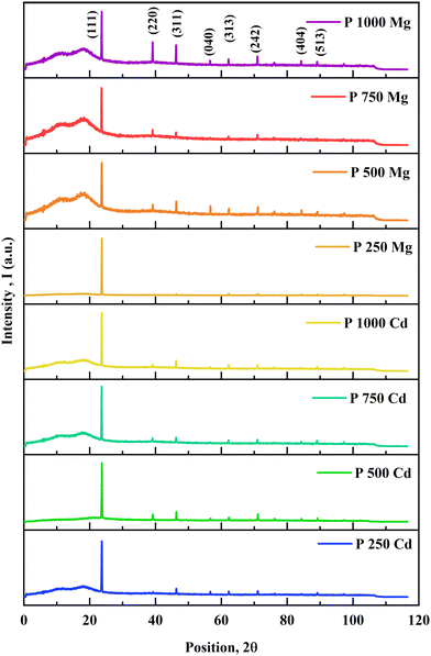
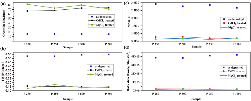
From the X-ray powder diffraction (XRD) data, the structural and crystallographic characteristics of the CdCl2 and MgCl2-treated CdTe films are investigated. X-ray diffraction as shown in Fig. 1 demonstrates that the deposited films are polycrystalline and the main diffraction peak, which corresponds to the crystal orientation at the (111) cubic plane according to JCPDS card number 96-900-8841, appears prominently at 2θ = 23.8° for all treated films. The (220) and (311) planes are represented by two additional small intensity peaks at latitudes 2θ = 39.29° and 2θ = 46.91°, respectively.15 The average crystallite sizes (D) of the films are determined by the Scherrer formula25–27 to provide additional structural features. However, it is depicted in Fig. 1 that some other less intense peaks are visible at (040), (313), (242), (404) and (513) for MgCl2-treated CdTe films.The estimated values of different microstructural parameters for CaCl2 and MgCl2-treated CdTe thin films are listed in Table 2. This illustrates significantly lower FHWM for all treated samples, which confirms larger crystallite size compared to the as deposited film.25 The average crystallite size for the CdCl2-treated film has simultaneously increased from 67 to 74 nm. And it ranges from 71 to 82 nm for MgCl2-treated CdTe samples,28 whereas it varies from 15 to 16 nm for as-deposited films.24 So obviously a drastic change in crystal size is observed.
| Sample | Position 2θ (deg) | d hkl (Å) | FWHM (deg) | Crystallite size, D (nm) | Dislocation density, δ × 1014 (lines per m2) | Strain, ε × 10−4 | Crystallite no, N × 1012 (m−2) | Degree of crystallinity (%) |
|---|---|---|---|---|---|---|---|---|
| P 250 Cd | 23.665 | 3.7566 | 0.1589 | 67 | 2.26 | 7.68 | 1.27 | 31.98 |
| P 500 Cd | 23.723 | 3.7475 | 0.1517 | 68 | 2.16 | 7.78 | 1.19 | 28.16 |
| P 750 Cd | 23.636 | 3.7611 | 0.1467 | 73 | 1.87 | 6.89 | 0.96 | 31.26 |
| P 1000 Cd | 23.665 | 3.7566 | 0.1428 | 74 | 1.82 | 6.90 | 0.92 | 31.19 |
| P 250 Mg | 23.694 | 3.7520 | 0.1281 | 82 | 1.50 | 6.38 | 0.69 | 35.17 |
| P 500 Mg | 23.636 | 3.7611 | 0.1768 | 73 | 1.87 | 6.89 | 0.96 | 31.68 |
| P 750 Mg | 23.578 | 3.7702 | 0.1384 | 80 | 1.58 | 6.13 | 0.75 | 30.70 |
| P 1000 Mg | 23.636 | 3.7611 | 0.1502 | 71 | 1.96 | 7.05 | 1.03 | 31.25 |
A comparison of the microstructural data among as-deposited and treated samples is depicted in Fig. 2(a) to (d). Studies reveal that smaller grains vanish and newly formed larger grains are seen after CdCl2 treatment.18,29 This mostly happens for low-temperature deposition (∼450 °C) when as-deposited particles are tiny and the grain size is greatly enhanced after Cl treatment.7 Consequently, it provides the benefits of larger crystallite size, lower dislocation density, and strain. Comparatively larger crystallite size is observed for MgCl2-treated samples. However, according to the study, for higher temperature deposition (∼620 °C) methods, with the probable exclusion of some near-CdS interface recrystallization, the as-deposited grain size is nearly comparable to the chloride-cured particle size.30 However, there might be grain growth or not, but the CdCl2 treatment results in a significant improvement in device effectiveness in both situations.5 It is possible that they're linked to intra-grain passivation instead in the case of high temperature CdTe film deposition.30 Additional research is being done to support this theory. In addition, 1.1 mm BSG has been used as a substrate for this experiment with a thermal expansion coefficient (CTE) of 3.3 × 10⁻⁶ K−1. The CTE of ultra-thin glass (UTG) is 7.2 × 10⁻⁶ K−1, which is close to the CTE of CdTe (5.9 × 10⁻⁶ K−1).31 The reduction of tensile or compressive stress during the cooling process following high temperature or pressure deposition can be achieved by employing a balanced CTE. Therefore, with high bendability and transparency, UTG would be a better substrate replacement with desirable qualities to avert surface stress and dislocation density.
The addition of chloride serves as an n-type dopant in CdTe. Upon annealing with CdCl2,32 the grain boundary (GB) states and electrical properties undergo notable changes. This occurs as chlorine atoms segregate and occupy tellurium sites at the grain boundary. For example, the Te–Te interaction undergoes a reduction in energy when it transforms into a Te–Cl interaction due to the isolation of one chlorine (Cl) atom per core within the grain boundary (GB).
This isolation causes the antibonding states to be further pushed into the energy range of the band gap. The Te–Cl antibonding states are partially occupied by extra electrons originating from the dopant atoms, resulting in the Cl atoms retaining a positive charge and creating an electrostatic potential. By reducing the energy of the occupied Cd–Cd bonding states, this potential causes them to approach the valence band maximum (VBM).24 The energies of the new antibonding states between Cl–Cl decrease notably as additional Cl atoms are introduced into the GB. As a result, the charge transfer enhances the electrostatic potential, leading to the downward displacement of the unoccupied Cd–Cd bonding states towards the valence band. Hence, it may be inferred that the presence of Cl segregation in all grain boundaries (GBs) will enhance their structural integrity, leading to the formation of a p–n–p junction across the GB.32 Electrons tend to separate along the grain boundaries, while holes are retained within the bulk of the grain. The rate of carrier recombination can be reduced by the built-in field that arises between the grain external (GB) and grain interior (GI) regions, as it assists in the separation of photo-generated carriers.17 The findings indicate that the bulk carrier density of the CdTe film subjected to MgCl2 treatment is equivalent to or greater than the bulk carrier density seen in films treated with CdCl2.
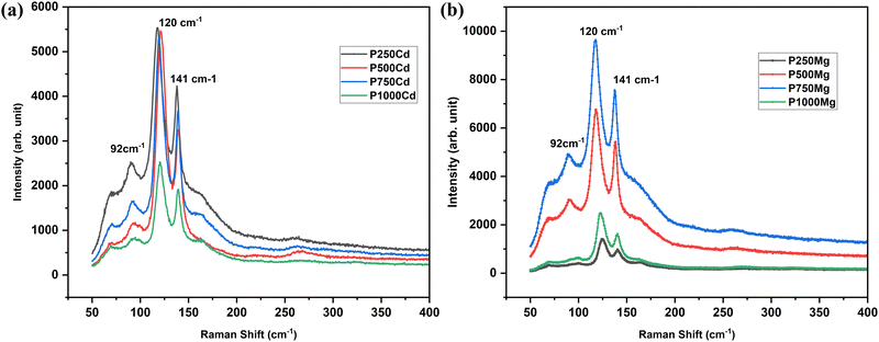
Raman spectra were recorded by using a 532 nm excitation wavelength for the samples prepared under different conditions followed by post-growth treatment by two types of chloride between 100 and 400 demonstrated in Fig. 3(a) and (b). Raman spectra are typically a unique chemical fingerprint for a certain molecule or material to rapidly characterize the chemical composition. Three discrete bands are seen in the spectrum at 92, 120, and 141 cm−1. The production of CdTe is demonstrated by the bands at 141, 163, and 330 cm−1. Elementary Te can be attributed to additional bands at 92 and 120 cm−1, which were not seen in the X-ray pattern.33 The emission peak at 120 cm−1 corresponds to the A1 mode of the Te Raman active peak. According to Soares et al.,34 the elemental Te band can be found in the CdTe spectra captured using micro-Raman techniques. It is demonstrated that Te aggregates are formed on the sample surface when CdTe is exposed to laser lines with shorter wavelengths than 840 nm. This is likely the cause of the Te signal being present in the Raman spectra but absent from XRD configurations. The next one at 141 cm−1 is attributed to an amalgamation of the CdTe's transversal optical (TO) phonon at 141 cm−1 and the Te peak E1(Te) at 139 cm−1.35 The CdTe longitudinal optical (LO) phonon is linked to the less intense detected peak at 167 cm−1 visible for a few samples in Fig. 3.36 Raman analysis performed for this work is just to confirm the material and the phase purity by rapidly characterizing the chemical composition of CdTe after post-growth treatment by two types of chloride.
3.2. SEM microstructure
The influence of Cl treatment on the surface morphology of CdTe films is considered using scanning electron microscopy (SEM). Fig. 4(a)–(h) displays the representative images. The dense and granular surface layer is observed for all the treated samples. The columnar-like structure and distinct growth texture, which are devoid of cracks and pinholes, indicate a high quality CdTe film. A completely new microstructure results from the Cl2 treatment of the CdTe thin film by re-crystallization, which causes some smaller grains to consolidate into superior ones while other larger grains to fragment into smaller ones and reorganize themselves.37 Smaller grains have greater activity and solubility in the melting flux, which enhances mass carrier movement.38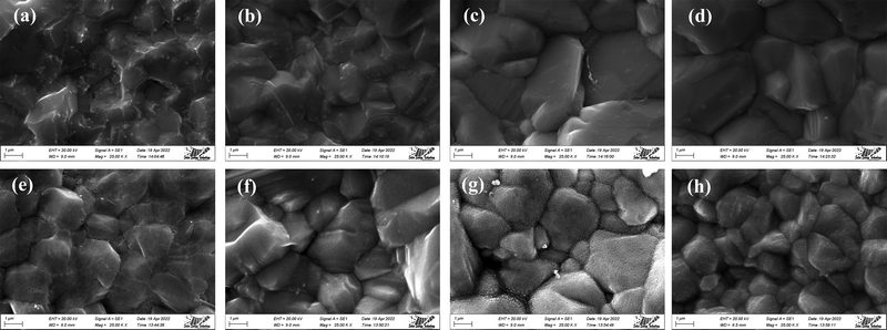 | ||
| Fig. 4 SEM images of CdTe films for (a) P 250 Cd, (b) P 500 Cd, (c) P 750 Cd, (d) P 1000 Cd, (e) P 250 Mg, (f) P 500 Mg, (g) P 750 Mg and (h) P 1000 Mg. | ||
When the sample is treated with MgCl2, the shape of the CdTe films considerably varied (Fig. 4(e)–(h)) in structure. The CdTe thin film treated with MgCl2 is composed of highly textured and incredibly sharper crystals that have been formed on the grains' surface compared to the CdCl2-treated film (Fig. 4(a)–(d)). In comparison to CdCl2-treated films, the MgCl2-treated film exhibits sharper crystals on the surface of the grains. This implies that the MgCl2 treatment has a more pronounced effect on crystal formation, leading to sharper and better-defined features. And that is the reason for the comparatively sharp peaks for XRD (Fig. 1) of MgCl2-treated CdTe films. The X-ray diffraction (XRD) analysis of the MgCl2-treated CdTe films shows comparatively sharp peaks. This indicates that the crystal structure in the MgCl2-treated films is more well-defined and organized compared to the CdCl2-treated films. The sharp peaks in XRD typically suggest a more crystalline and ordered structure. In addition, the SEM image presents the average grain size whereas XRD analysis displays measurements relating to crystallite size within the grain.29 The grain sizes may also vary depending on the growth technique25 and conditions,39 which is reported in previous communications.1,24
The impact of chloride treatment on grain boundaries is highly significant, warranting further investigation and study. An accepted concept in solid-state chemistry is that the addition of impurities lowers a material's or compound's melting point. Several contaminants are added to the CdTe surface during the chloride treatment process. Among these are excess elemental Te deposited during development, excess Cd and Cl from CdCl2, and O from air annealing.
Furthermore, there will be CdTe crystallites or amorphous CdTe present in the grain boundaries. The melting point of grain boundary materials will be significantly lowered by all of the aforementioned impurities to a heat treatment temperature range of around 350–450 °C. Large CdTe crystals will therefore continue to exist as solid materials while the components near the grain boundaries will melt into a liquid. This melting temperature has previously been determined to be 385 ± 5 °C.40 At this point, the thin film abruptly transforms into a group of CdTe crystals floating atop a thin liquid layer that has developed along grain boundaries. When heat treated and then cooled, the CdTe layers produced with (111) preferred orientation abruptly shift as a result of crystals floating in a liquid phase displaying random nature of crystalline orientation. Following this procedure, the majority of the CdTe crystals exhibit columnar character as they expand over the thin film thickness. Convection currents cause the liquid to move freely along grain boundaries during heating, allowing all of the constituents to mix properly, react chemically, and maybe even evaporate from the liquid in excess. Within grain boundaries, excess Cd from CdCl2 and any elemental Te available can form a CdTe compound. Other elements present, such as Cl, O, and other elements, dope this material to give it a specific electrical conductivity. The CdTe crystals stay solid after cooling, and the material at the grain boundary becomes hardened without creating any pinholes in the thin film in order to create superior solar cells. The introduction of both these features occurs during the CdCl2 treatment of ED-CdTe, leading to a significant impact.41 On the other hand, massive crystals in the μm-scale have already been created using high-temperature grown CSS-CdTe.40 So, the addition or enhancement has a relatively smaller impact there. However, there is still a benefit to the chloride therapy.
3.3. Composition
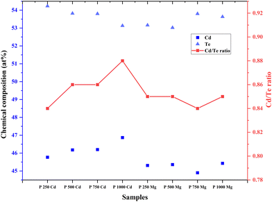
According to the EDS spectrogram, all of the samples have similar Cd and Te dominance and authenticate the steadiness of the CdTe thin film through different deposition conditions and treatment. Fig. 5 displays the atomic percentages of Cd, Te, and Cd/Te ratio for the samples. Both CdCl2 and MgCl2-treated CdTe thin films displayed a nearly stoichiometric Cd/Te ratio (ratio from 0.84 to 0.88).33 The results again conclude that CdCl2 is replaceable with MgCl2. However, it is noteworthy that for Cd-treated samples, the Cd/Te ratio varies from 0.84–0.88. And for the Mg-treated sample the ratio varied from 0.84–0.85. The CdCl2-treated samples as expected show a comparatively higher Cd atomic percentage than the MgCl2 treated CdTe films. However, Ojo et al.42 reported an interesting insight that electrodeposited p-type CdTe, rich in Te and n-type CdTe, rich in Cd, together (n–n–p configuration) offer the best efficiency of 15.3% where any treatment was skipped. It is widely known from studies on semi-insulating CdTe that Te precipitation forms in CdTe regardless of the synthesis process.43 The precipitation of Te occurs during the formation of CdTe due to Te's usual comportment and is recognized to be the root of the poor electrical feature of Te-rich CdTe.44 The precipitated Te is removed by Cl2 treatment and annealing. CdTe-based solar cells typically benefit from excess tellurium or precipitated cadmium. Studies show that stoichiometric deviation might alter the band gap of a material.29 The aforementioned findings are in accordance with earlier research41,42 and it further demonstrates that the CdTe stoichiometry plays a vital role in cell efficiency. Therefore, it might be concluded that MgCl2 treatment would be more beneficial to achieve high-efficiency CdTe solar cells.3.4. Optical analysis
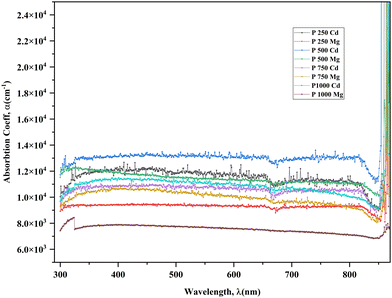
A study of the treated CdTe films' optical attributes is intended to investigate their energy band gap, Urbach energy (EU), refractive index (n), and extinction coefficient (k) for better understanding. The calculation for estimating these optical parameters is described in a previous report.24 By computing the absorbance of CdTe films, optical properties are examined. In order to mitigate the impact of the fundamental substrate, the absorbance of the reference glass is nullified. Fig. 6 illustrates that the samples treated with CdCl2 exhibit nearly uniform absorbance across the visible wavelength spectrum. The absorption coefficient (α) value is approximately 104 cm−1, which confirms the anticipated absorbance of over 90% for an effective absorber layer. However, MgCl2-treated samples show comparatively low absorbance (∼88%). It is also a suggestion of the thickness consistency of placed films.45 However, Fig. 6 depicts that CdCl2 and MgCl2-treated samples show comparatively lower absorption coefficient, α than that of as deposited CdTe films.24,29 For calculating the absorption coefficient the following classic equation46 is used. | (1) |
In this context, the variable n represents a constant that can take on the values of 1/2, 2, 3/2, or 3. The specific value of n depends on the type of transition being considered, namely allowed direct, allowed indirect, forbidden direct, or forbidden indirect transitions. The absorbance, which is extremely reliant on the category of surface modification being employed, determines the absorption coefficient. As a result, expanding the absorption area could further improve the value that was achieved. This can be done by decreasing the hole widths, or growing the density of holes, and their depths.36
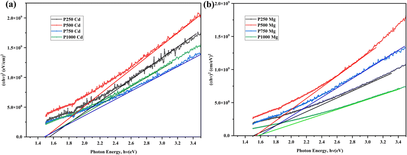
The Tauc plots derived from the investigational data are shown in Fig. 7(a) and (b). It is possible to determine the energy band gap by extrapolating the linear fit at the absorption limit, α = 0. The estimated optical energy band gap of the aforementioned CdTe thin films ranges between 1.48–1.60 eV tabulated in Table 3, in good agreement with previous outcomes.13,42 For this study, the incorporation of Cl treatment for post-annealing, induces an insignificant band gap variation, as no clear trends can be observed. Nevertheless, it can be considered that Cl treatment does not have a substantial conclusion on the band gap for the CdTe films either by CdCl2 or MgCl2. Table 3 presents the values of the band gap, refractive index, and dielectric constant of the CdTe thin films that were produced under various argon pressures and subsequently subjected to selective chloride treatment. The obtained results are all in good agreement with former reports.29
| Sample | Band gap, Eg (eV) | Refractive index, n | High frequency dielectric cont., ε∞ | Dielectric cont., ε0 |
|---|---|---|---|---|
| P 250 Cd | 1.56 | 2.885 | 8.321 | 13.715 |
| P 500 Cd | 1.50 | 2.913 | 8.485 | 13.900 |
| P 750 Cd | 1.48 | 2.923 | 8.542 | 13.962 |
| P 1000 Cd | 1.49 | 2.918 | 8.514 | 13.931 |
| P 250 Mg | 1.50 | 2.913 | 8.485 | 13.900 |
| P 500 Mg | 1.53 | 2.899 | 8.402 | 13.808 |
| P 750 Mg | 1.60 | 2.866 | 8.216 | 13.592 |
| P 1000 Mg | 1.55 | 2.889 | 8.347 | 13.746 |
When compared to untreated samples, treated samples exhibit an increment in the refractive index and a minor drop in transmittance. Here, there are no discernible changes in refractive index. This might be because the treated samples have the same optical band gap and thickness.29
The spectral dependence of the absorption coefficient, with respect to photon energies (hν) that are lower than the energy band-gap of a CdTe thin film, can be described by
α = α0![[thin space (1/6-em)]](https://www.rsc.org/images/entities/char_2009.gif) exp(E/EU) exp(E/EU) | (2) |
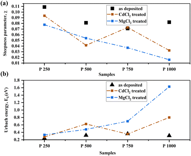 | ||
| Fig. 8 Urbach energy (bottom) and steepness parameter, σ (top) of CdCl2 and MgCl2-treated CdTe thin film. | ||
The determination of skin depth arises from the substantial dependence of conductivity in semiconducting materials on the optical band gap.
 | (3) |
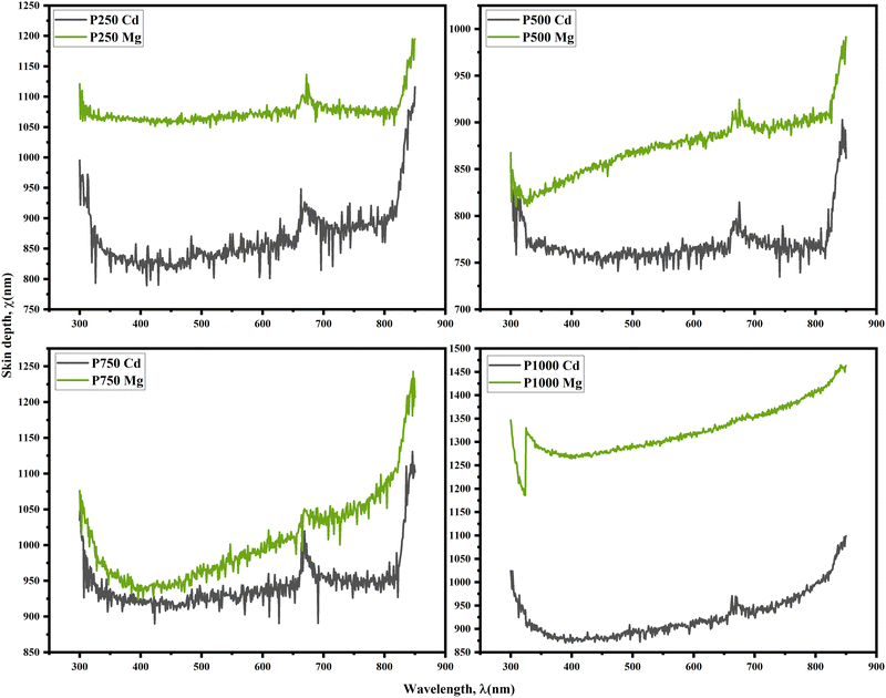
In this context, the symbol χ represents the skin depth, which refers to the depth at which the electromagnetic field intensity decreases by a factor of e−1. On the other hand, α denotes the absorption coefficient of the thin film, which quantifies the extent to which the film absorbs incident electromagnetic radiation. There exists a correlation between the square root of the resistivity of a good conductor and the variable χ. Consequently, materials with higher conductivity have shallower skin depths. The dependency of χ on incident light wavelength for CaCl2 and MgCl2-treated CdTe thin films is revealed in Fig. 9. χ seems to be high in the ultraviolet range; however, it rapidly drops and stabilizes as the wavelength increases in the visible zone. There is an abrupt change near the wavelength of 700 nm, which is expected due to the detector change of the UV-Vis spectrometer. Moreover, it demonstrates that all the CdTe samples treated with CdCl2 show smaller values of χ and the MgCl2-treated CdTe films possess greater values. This again confirms higher absorption by CdCl2-treated CdTe thin films. So it can be concluded that the films with higher absorbance have lower χ, which provides an idea of why high absorption reduces the film's transmittance and restricts the amount of light that may pass through it.
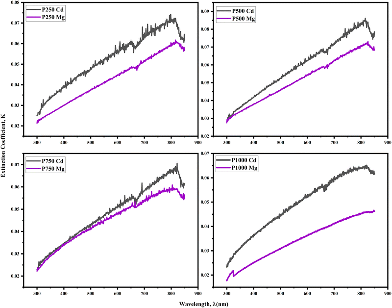
Fig. 10 illustrates the relationship between the extinction coefficient (K)50 of the thin CdTe film treated with CdCl2 and MgCl2. K has a lower value in the ultraviolet region; however, it increases linearly as the wavelength increases in the visible range. Here, the abrupt modification of K near 700 nm is again visible. For spectrometers with dual detectors, this behavior is typical. The mechanical alignment of both detectors must be perfect, and the intensity of light output must be adjusted to avoid it. Additionally, Fig. 10 demonstrates that all the CdTe samples treated with CdCl2 had greater values of K and the MgCl2-treated CdTe films possess smaller values of that. This behavior may be in agreement with Fig. 6 because it is exactly relational to α and the material width of the film. The lower values of K signify a thin film's surface that is relatively smoother and less likely to lose light energy through scattering and absorption. So here we can conclude that the best performance is expected from MgCl2-treated absorber CdTe films as they lose less light.
4. Conclusions
The major commercially credible alternative option to silicon-based solar technology is now CdTe thin-film solar cells. This communication effort effectively integrated the knowledge by assessment of two effective chloride treatments with MgCl2 and conventional CdCl2. It is demonstrated that the modification of the grain boundaries by chlorine results in an upsurge in structural attributes. Therefore, to attain high conversion efficiencies, the performance of the CdTe absorber layer relies on the chloride activation process as it enhances its structural n optical properties. The reported work presents experimental findings in favor of a non-toxic, environmentally friendly MgCl2 therapy, which can substitute CdCl2. For the CdCl2 treated film, the average crystallite size synchronously expanded from 67 to 74 nm. Additionally, it varies from 71 to 82 nm for MgCl2-treated CdTe samples. SEM analysis suggests that the MgCl2 treatment affects crystal formation more strongly, producing characteristics that are more defined and sharp. However, the MgCl2-treated samples have higher Urbach energy and skin depth and lower extinction coefficient. It is further demonstrated that film stoichiometry can also be controlled with these treatments to achieve p or n-type CdTe films depending on the module configuration. Consequently, concentrating on better or more regulated grain boundary treatments would offer a way to increase the cell voltages and hence power conversion efficiency. Considering structural and other physical properties, MgCl2 might be a perfect alternative to CdCl2 for manufacturing use as it is non-toxic and ecologically sound. Nevertheless, it is demonstrated in this study that there is still room for advancement. The CdCl2 treatment in the presence of oxygen, according to scientific literature, results in superior devices. To comprehend this processing step, it is important to thoroughly investigate the presence of oxygen in the material and finally, the MgCl2-treated device configuration. A comprehensive investigation is also needed on the impact of Cd richness in removing Te-precipitation in CdTe focusing on XPS, AFM and electrical analysis. In this manner, the next work is proceeding.Data availability
The dataset generated during analysis during the current study is available from the corresponding author on reasonable request.Author contributions
AS – formal analysis, investigation, methodology, visualization, writing – original draft; SSM – investigation, methodology; MS – investigation, visualization; MAAS – funding acquisition, writing & editing; and MSB – conceptualization, supervision, resources, investigation, project administration.Conflicts of interest
This work has been executed at our laboratory as a locally funded project as acknowledged accordingly. No conflict of interest exists with any parties other than acknowledged in the acknowledgment section.Acknowledgements
The authors would like to thank the Institute of Energy Research and Development (IERD) former Institute of Fuel Research and Development (IFRD) of Bangladesh Council of Scientific and Industrial Research (BCSIR) for all the support for this research work. This work is supported by the Bangladesh Council of Scientific and Industrial Research (BCSIR), Ministry of Science and Technology, Bangladesh, through the research and development project grant scheme (ref: 39.02.0000.011.14.134.2021.388; dt: 21-09-2021) entitled ‘Increasing the photo-conversion efficiency of CdTe-based solar cell by selective Cl-treatment.’References
- N. Amin, M. R. Karim and Z. A. Alothman, An In-Depth Analysis of CdTe Thin-Film Deposition on Ultra-Thin Glass Substrates via Close-Spaced Sublimation (CSS), Coatings, 2022, 12(5), 589, DOI:10.3390/coatings12050589.
- I. O. Oladeji, L. Chow, C. S. Ferekides, V. Viswanathan and Z. Zhao, Metal/CdTe/CdS/Cd1-xZnxS/TCO/glass: A new CdTe thin film solar cell structure, Sol. Energy Mater. Sol. Cells, 2000, 61(2), 203–211, DOI:10.1016/S0927-0248(99)00114-2.
- M. A. Green, E. D. Dunlop, J. Hohl-Ebinger, M. Yoshita, N. Kopidakis and X. Hao, Solar cell efficiency tables (Version 58), Prog. Photovoltaics Res. Appl., 2021, 29(7), 657–667, DOI:10.1002/PIP.3444.
- M. A. Scarpulla, B. McCandless, A. B. Phillips, Y. Yan, M. J. Heben, C. Wolden, G. Xiong, W. K. Metzger, D. Mao, D. Krasikov, I. Sankin, S. Grover, A. Munshi, W. Sampath, J. R. Sites, A. Bothwell, D. Albin, M. O. Reese, A. Romeo, M. Nardone, R. Klie, J. M. Walls, T. Fiducia, A. Abbas and S. M. Hayes, CdTe-based thin film photovoltaics: Recent advances, current challenges and future prospects, Sol. Energy Mater. Sol. Cells, 2023, 255, 112289 CrossRef CAS.
- I. M. Dharmadasa, Review of the CdCl2 treatment used in CdS/CdTe thin film solar cell development and new evidence towards improved understanding, Coatings, 2014, 4(2), 282–307, DOI:10.3390/coatings4020282.
- J. Ma, S. H. Wei, T. A. Gessert and K. K. Chin, Carrier density and compensation in semiconductors with multiple dopants and multiple transition energy levels: Case of Cu impurities in CdTe, Phys. Rev. B: Condens. Matter Mater. Phys., 2011, 83, 1–7, DOI:10.1103/PhysRevB.83.245207.
- J. D. Major, Grain boundaries in CdTe thin film solar cells: A review, Semicond. Sci. Technol., 2016, 31(9), 1–19, DOI:10.1088/0268-1242/31/9/093001.
- B. E. McCandless, L. V. Moulton and R. W. Birkmire, Recrystallization and sulfur diffusion in CdCl2-treated CdTe/CdS thin films, Prog. Photovoltaics Res. Appl., 1997, 5, 249–260 CrossRef CAS.
- H. R. Moutinho, M. M. Al-Jassim, F. A. Abulfotuh, D. H. Levi, P. C. Dippo, R. G. Dhere and L. L. Kazmerski, Studies of recrystallization of CdTe thin films after CdCl2 treatment, Conference Record of the IEEE Photovoltaic Specialists Conference, 1997, pp. 431–434 Search PubMed.
- P. R. Edwards, S. A. Galloway and K. Durose, EBIC and luminescence mapping of CdTe/CdS solar cells, Thin Solid Films, 2000, 361–362, 364–370 CrossRef CAS.
- Y. Y. Proskuryakov, K. Durose, B. M. Taele and S. Oelting, Impedance spectroscopy of unetched CdTe/CdS solar cells-equivalent circuit analysis, J. Appl. Phys., 2007, 102(2) DOI:10.1063/1.2757011.
- J. D. Major, Y. Y. Proskuryakov and K. Durose, Impact of CdTe surface composition on doping and device performance in close Space sublimation deposited CdTe solar cells, Prog. Photovoltaics Res. Appl., 2013, 21, 436–443, DOI:10.1002/PIP.1196.
- S. Chander and M. S. Dhaka, Time evolution to CdCl2 treatment on Cd-based solar cell devices fabricated by vapor evaporation, Sol. Energy, 2017, 150, 577–583, DOI:10.1016/j.solener.2017.05.013.
- V. A. Gevorgyan, N. R. Mangasaryan, V. F. Gremenok, M. S. Tivanov, P. Thakur, A. Thakur, S. V. Trukhanov, T. I. Zubar, M. I. Sayyed, D. I. Tishkevich and A. V. Trukhanov, Morphology and structure of CdCl2-Containing CdTe films deposited by discrete vacuum thermal evaporation, Vacuum, 2023, 214, 112248, DOI:10.1016/j.vacuum.2023.112248.
- S. L. Patel, Himanshu, S. Chander, M. D. Kannan and M. S. Dhaka, Impact of chloride treatment on the physical properties of polycrystalline thin CdTe films for solar cell applications, Phys. Lett. Sect. A Gen. At. Solid State Phys., 2019, 383(15), 1778–1781 CAS.
- N. Romeo, A. Bosio and A. Romeo, An innovative process suitable to produce high-efficiency CdTe/CdS thin-film modules, Sol. Energy Mater. Sol. Cells, 2010, 94, 2–7, DOI:10.1016/J.SOLMAT.2009.06.001.
- J. D. Major, M. Al Turkestani, L. Bowen, M. Brossard, C. Li, P. Lagoudakis, S. J. Pennycook, L. J. Phillips, R. E. Treharne and K. Durose, In-depth analysis of chloride treatments for thin-film CdTe solar cells, Nat. Commun., 2016, 7 DOI:10.1038/ncomms13231.
- S. Chander and M. S. Dhaka, CdCl2 treatment concentration evolution of physical properties correlation with surface morphology of CdTe thin films for solar cells, Mater. Res. Bull., 2018, 97, 128–135, DOI:10.1016/j.materresbull.2017.08.038.
- K. A. Aris, K. S. Rahman, A. M. Ali, B. Bais, I. Bin Yahya, M. Akhtaruzzaman, H. Misran, S. F. Abdullah, M. A. Alghoul and N. Amin, A comparative study on thermally and laser annealed copper and silver doped CdTe thin film solar cells, Sol. Energy, 2018, 173, 1–6, DOI:10.1016/j.solener.2018.07.009.
- Y. Qu, P. V. Meyers and B. E. McCandless, HCl vapor post-deposition heat treatment of CdTe/CdS films, Conference Record of the IEEE Photovoltaic Specialists Conference, 1996, pp. 1013–1016 DOI:10.1109/PVSC.1996.564303.
- J. D. Major, R. E. Treharne, L. J. Phillips and K. Durose, A low-cost non-toxic post-growth activation step for CdTe solar cells, Nature, 2014, 511, 334–337, DOI:10.1038/nature13435.
- J. D. Major, L. Bowen, R. E. Treharne, L. J. Phillips and K. Durose, NH4Cl alternative to the CdCl2 treatment step for CdTe thin-film solar cells, IEEE J. Photovoltaics, 2015, 5, 386–389, DOI:10.1109/JPHOTOV.2014.2362296.
- S. L. Patel, S. Chander, A. Purohit, M. D. Kannan and M. S. Dhaka, Influence of NH4Cl treatment on physical properties of CdTe thin films for absorber layer applications, J. Phys. Chem. Solids, 2018, 123, 216–222, DOI:10.1016/j.jpcs.2018.07.021.
- C. Li, Y. Wu, J. Poplawsky, T. J. Pennycook, N. Paudel, W. Yin, S. J. Haigh, M. P. Oxley, A. R. Lupini, M. Al-Jassim, S. J. Pennycook and Y. Yan, Grain-boundary-enhanced carrier collection in CdTe solar cells, Phys. Rev. Lett., 2014, 112, 1–5, DOI:10.1103/PhysRevLett.112.156103.
- A. Sharmin, S. S. Mahmood, M. Sultana, S. Aziz, M. A. A. Shaikh and M. S. Bashar, Effect of argon pressure on the physical characteristics of cadmium telluride (CdTe) thin films by close-spaced sublimation, J. Mater. Sci.: Mater. Electron., 2023, 34(5) DOI:10.1007/s10854-022-09603-w.
- V. D. Falcão, W. A. Pinheiro, C. L. Ferreira and L. R. de Oliveira Cruz, Influence of deposition parameters on the properties of CdTe films deposited by close spaced sublimation, Mater. Res., 2006, 9, 29–32, DOI:10.1590/S1516-14392006000100007.
- R. Mis-Fernández, I. Rimmaudo, V. Rejón, E. Hernandez-Rodriguez, I. Riech, A. Romeo and J. L. Peña, Deep study of MgCl2 as activator in CdS/CdTe solar cells, Sol. Energy, 2017, 155, 620–626, DOI:10.1016/j.solener.2017.06.061.
- S. L. Patel, Himanshu, A. Purohit, S. Chander, M. D. Kannan and M. S. Dhaka, Thermal evolution to MgCl2 activation on physical properties of CdTe thin films for solar cell applications, AIP Conf. Proc., 2020, 2265 DOI:10.1063/5.0017266.
- N. Amin, M. R. Karim and Z. A. ALOthman, Impact of CdCl2 treatment in CdTe thin film grown on ultra-thin glass substrate via close-spaced sublimation, Crystals, 2021, 11, 1–16 Search PubMed.
- J. Quadros, A. L. Pinto, H. R. Moutinho, R. G. Dhere and L. R. Cruz, Microtexture of chloride treated CdTe thin films deposited by CSS technique, J. Mater. Sci., 2008, 43, 573–579, DOI:10.1007/s10853-007-1708-5.
- G. Abadias, E. Chason, J. Keckes, M. Sebastiani, G. B. Thompson, E. Barthel, G. L. Doll, C. E. Murray, C. H. Stoessel and L. Martinu, Review Article: Stress in thin films and coatings: Current status, challenges, and prospects, J. Vac. Sci. Technol., A, 2018, 36, 020801, DOI:10.1116/1.5011790.
- M. Tuteja, P. Koirala, V. Palekis, S. Maclaren, C. S. Ferekides, R. W. Collins and A. A. Rockett, Direct Observation of CdCl2 Treatment Induced Grain Boundary Carrier Depletion in CdTe Solar Cells Using Scanning Probe Microwave Reflectivity Based Capacitance Measurements, J. Phys. Chem. C, 2016, 120, 7020–7024, DOI:10.1021/acs.jpcc.6b00874.
- M. Osial, J. Widera and K. Jackowska, Influence of electrodeposition conditions on the properties of CdTe films, J. Solid State Electrochem., 2013, 17, 2477–2486, DOI:10.1007/s10008-013-2125-0.
- M. J. Soares, J. C. Lopes, M. C. Carmo and A. Neves, Micro-Raman study of laser damage in CdTe, Phys. Status Solidi C Conf., 2004, 1, 278–280, DOI:10.1002/pssc.200303931.
- L. P. Rivera, E. García, D. Cardona, A. Pérez-Centeno, E. Camps, M. A. Santana-Aranda, G. Gómez-Rosas, F. De Moure-Flores, A. Chávez-Chávez and J. G. Quiñones-Galván, CdTe:Sn thin films deposited by the simultaneous laser ablation of CdTe and Sn targets, Mater. Res. Express, 2019, 7, 15905, DOI:10.1088/2053-1591/ab6119.
- J. Rangel-Cárdenas and H. Sobral, Optical absorption enhancement in CdTe thin films by micro structuration of the silicon substrate, Materials, 2017, 10(6) DOI:10.3390/ma10060607.
- Q. G. Zhang, X. Zhang, B. Y. Cao, M. Fujii, K. Takahashi and T. Ikuta, Influence of grain boundary scattering on the electrical properties of platinum nanofilms, Appl. Phys. Lett., 2006, 89, 114102, DOI:10.1063/1.2338885.
- N. Spalatu, J. Hiie, V. Valdna, M. Caraman and N. Maticiuc, Properties of the CdCl2 air-annealed CSS CdTe thin films, Energy Procedia, 2020, 44, 85–95, DOI:10.1016/j.egypro.2013.12.013.
- S. Kumari, D. Suthar, Himanshu, N. Kumari and M. S. Dhaka, Understanding Grain Growth Mechanism in Vacuum Evaporated CdTe Thin Films by Different Halide Treatments: An Evolution of Ion Size Impact on Physical Properties for Solar Cell Applications, Comments Inorg. Chem., 2023, 43(6), 429–464 CrossRef CAS.
- I. M. Dharmadasa, A. E. Alam, A. A. Ojo and O. K. Echendu, Scientific complications and controversies noted in the feld of CdS/ CdTe thin flm solar cells and the way forward for further development, J. Mater. Sci.: Mater. Electron., 2019 DOI:10.1007/s10854-019-02422-6.
- A. E. Alam, O. I. Olusola, D. A. L. Loch, K. Shukla, W. M. Cranton and I. M. Dharmadasa, Electrodeposition of ternary compounds for novel PV application and optimisation of electrodeposited CdMnTe thin – films, Sci. Rep., 2020, 1–13, DOI:10.1038/s41598-020-78066-y.
- A. A. Ojo and I. M. Dharmadasa, 15.3% efficient graded bandgap solar cells fabricated using electroplated CdS and CdTe thin films, Sol. Energy, 2016, 136, 10–14, DOI:10.1016/j.solener.2016.06.067.
- M. Ayoub, M. Hage-Ali, J. M. Koebel, A. Zumbiehl, C. Rit, R. Regal, F. Klotz, P. Siffert and P. Fougeres, Annealing Effects on Defect Levels of CdTe: Cl Materials and the Uniformity of the Electrical Properties, IEEE Trans. Nucl. Sci., 2003, 50, 229–237, DOI:10.1109/TNS.2003.809981.
- S. P. Harvey, G. Teeter, H. Moutinho and M. M. Al-Jassim, Direct evidence of enhanced chlorine segregation at grain boundaries in polycrystalline CdTe thin films via three-dimensional TOF-SIMS imaging, Prog. Photovoltaics Res. Appl., 2015, 23, 838–846, DOI:10.1002/PIP.2498.
- R. Yavorskyi, L. Nykyruy, G. Wisz, P. Potera, S. Adamiak and S. Górny, Structural and optical properties of cadmium telluride obtained by physical vapor deposition technique, Appl. Nanosci., 2019, 9, 715–724, DOI:10.1007/s13204-018-0872-z.
- A. Sharmin, S. Tabassum, M. S. Bashar and Z. H. Mahmood, Depositions and characterization of sol–gel processed Al-doped ZnO (AZO) as transparent conducting oxide (TCO) for solar cell application, J. Theor. Appl. Phys., 2019, 13, 123–132, DOI:10.1007/s40094-019-0329-0.
- K. Nagaya, S. Fujimoto, H. Tampo, S. Kim, M. Nishiwaki, Y. Nishigaki, M. Kato, H. Shibata and H. Fujiwara, Very small tail state formation in Cu2ZnGeSe4, Appl. Phys. Lett., 2018, 113(9) DOI:10.1063/1.5031799.
- M. S. Bashar, R. Matin, M. Sultana, A. Siddika, M. Rahaman, M. A. Gafur and F. Ahmed, Effect of rapid thermal annealing on structural and optical properties of ZnS thin films fabricated by RF magnetron sputtering technique, J. Theor. Appl. Phys., 2020, 14(1), 53–63, DOI:10.1007/s40094-019-00361-5.
- J. Chantana, Y. Kawano, T. Nishimura, A. Mavlonov and T. Minemoto, Impact of Urbach energy on open-circuit voltage deficit of thin-film solar cells, Sol. Energy Mater. Sol. Cells, 2020, 210, 110502, DOI:10.1016/j.solmat.2020.110502.
- W. W. Yu, L. Qu, W. Guo and X. Peng, Experimental determination of the extinction coefficient of CdTe, CdSe, and CdS nanocrystals, Chem. Mater., 2003, 15, 2854–2860, DOI:10.1021/cm034081k.
| This journal is © The Royal Society of Chemistry 2024 |

