
 Open Access Article
 This Open Access Article is licensed under a Creative Commons Attribution-Non Commercial 3.0 Unported Licence
Zinc(II)-heteroligand compounds for wet processing OLEDs: a study on balancing charge carrier transport and energy transfer†
Emmanuel Santos
Moraes‡
 ab,
Luís Gustavo Teixeira Alves
Duarte‡
b,
Fabiano Severo
Rodembusch
c,
José Carlos
Germino‡
*a,
Luiz Fernando Ribeiro
Pereira
*a and
Teresa Dib Zambon
Atvars
*b
ab,
Luís Gustavo Teixeira Alves
Duarte‡
b,
Fabiano Severo
Rodembusch
c,
José Carlos
Germino‡
*a,
Luiz Fernando Ribeiro
Pereira
*a and
Teresa Dib Zambon
Atvars
*b
aDepartment of Physics and i3N-Institute for Nanostructures, Nanomodeling and Nanofabrication, University of Aveiro, 3810-193 Aveiro, Portugal. E-mail: germino@ua.pt; luiz@ua.pt
bChemistry Institute, University of Campinas, Campinas 13083-970, Brazil. E-mail: tatvars@unicamp.br
cGrupo de Pesquisa em Fotoquímica Orgânica Aplicada, Instituto de Química (UFRGS), Av. Bento Gonçalves, 9500, CEP 91501-970 Porto Alegre, RS, Brazil
First published on 4th September 2024
Abstract
Organic light-emitting diodes (OLEDs) are one of the most studied and utilized optoelectronic components in display technology. However, their application in lighting remains limited due to materials costs and a guaranteed feasible deposition technique. To address this challenge, we explored the use of easily synthesized organic molecules capable of complexation with abundant transition metals to enhance their optoelectronic properties, coupled with low-cost wet processing protocols. Four zinc(II) coordination compounds were synthesized and the impact of incorporating two different ligands into a metal center was evaluated in terms of their optoelectronic properties. A photophysical investigation was made, encompassing emission and absorption analyses in both solid-state and thin film configurations. Förster resonance energy transfer (FRET) processes were performed using polyfluorene (PFO) and zinc(II) compounds in a host–guest system, revealing FRET efficiencies ranging from 10 to 68%, depending on the concentration of zinc(II) compounds in the PFO matrix. Subsequently, solution-processed OLEDs were fabricated using PFO:zinc(II) homo (ZnL11 and ZnL22) and heteroligand (ZnL13 and ZnL23) compounds as the emissive layer at a concentration of 1%, following a straightforward architecture, ITO|PEDOT:PSS|PVK|PFO:Zn(II)-compounds|TmPyPB|Ca|Al. The OLEDs achieved external quantum efficiencies (EQE) close to the theoretical limit of these active layers, ranging from 1.2% to 1.8%, with an applicable brightness value (L > 100 cd m−2), coupled with low roll-off in EQE values. Notably, the heteroligand coordination compounds exhibited superior device performance, attributed to their high electrical charge-carrier mobilities, trap-state profiles, and density of free carriers, as elucidated by space-charge shallow- (SCLC) and deep-trap (TCLC) transport models.
1. Introduction
Organic light-emitting diodes (OLEDs) synthesized by solution-processing techniques have emerged as promising alternatives to traditional thermally evaporated devices for producing low energy-consuming large area emitters.1 For solution-processed OLEDs, the active layers can be deposited by several wettable methods, such as spin-coating,2 slot-die coating,3 blade coating,4 and inkjet printing5 methods, offering scalable and straightforward implementation. However, there are several drawbacks to achieving a reasonable device performance. One is specially related to the design of active molecules with reasonable simple synthetic processes and with good emission properties; others are related to their solubility in commercial inexpensive solvents, which aids in achieving stable and uniform morphologies (without creation of intrinsic defects acting as energetic traps for electrical carriers), chemical and photochemical stabilities and reasonable charge mobility in the solid state.6 The best way to produce solution-deposited OLED active layers is still based on the host:guest concept.7To disperse an emissive molecule in such active layers, it is critical to choose solubility-compatible host–guest materials, ensuring proper charge-carrier injection, transport, and recombination from the host matrix to the guest emissive target.8,9 To improve the efficiency of host–guest systems, the energy levels of the components must fulfill the requirements for Förster/Dexter energy transfer, creating cascade channels for charge mobility and energy transfer processes, alongside a good molecular conformation.10,11
In recent decades, the external quantum efficiency (EQE) has increased substantially for solution-processed OLEDs.12 For instance, for thermal-evaporated OLEDs, Wang et al. obtained a red device based on the Pt(II) phosphorescent compound, composed of five evaporated layers between the electrodes, which resulted in a good EQE of 31.8%.13 Additionally, Pt(II) complex solution-processed OLEDs, which possess simpler architectures (with three or two layers), achieved EQEs of 22.9% and 15.0%, respectively14,15 Therefore, the production of stable materials for high-performance OLEDs must lead to the development of strategies toward the use of low-temperature protocols and simpler device architectures.
In this context, coordination compounds are a very wide class of OLEDs’ active layers. They might be composed of two categories: compounds with prevalent emission of the ligand and those with inner transition metal emission, singlet emission, or triplet emission. Because these metal–ligand properties define the emission process, there are several combinations of the same metallic center with ligands to provide unique materials and properties. Coordination compounds, encompassing ligand-based and metal-based emissions, offer a wide range of possibilities for OLED active layers.16–19 However, although heavy metals, such as iridium(III),20 platinum(II),15 osmium(III),21 ruthenium22 and rhenium23 complexes, can exhibit good performance, their cost, toxicity, and availability in nature are the main drawbacks leading to the choice of abundant metals, such as zinc(II).24
Zinc(II) complexes, which have versatile coordination geometries, have been demonstrated to be a promising candidates for active layer components, due to their desirable physical–chemical properties such as solubility, thermal stability, and fluorescence quantum yields.24–26 Despite their limitations in terms of internal quantum efficiency, zinc(II) complexes have already proven to achieve nearly 5% EQE values (the theoretical maximum values expected for such 1st generation emitters), almost close to the limit for singlet emission.27 In general, Zn(II) compounds are stable, with good solubilities, and can be easily synthesized, and the emission originated from the ligand. Improvement of the device performance can be achieved by the optimization of the charge transport mobility.19
In this sense, and seeking for solution-processed materials, we report the preparation and characterization of four zinc(II) complexes with two ligands to determine the role of their chemical structures in the figures of merit of OLEDs with active layers containing such complexes as emitters. The ligands (L1 and L2) are based on a salicylidene derivative that differs in the insertion of a bromine atom, forming ZnL11 and ZnL22 (homoligand) compounds and ZnL13 and ZnL23 are compounds with one ligand L1 or L2 and a 2-(2′-tosylaminophenyl) benzothiazole moiety (L3), forming structures L13 and L23 (heteroligand) (Fig. 1). Due to the solubility issues in solution-processed OLEDs, to improve optoelectronic properties without inserting another compound, two different ligands (L1–L3 and L2–L3) were used to improve the optoelectronic properties without changing the photophysical properties of the zinc(II) complex (L1–L1 and L2–L2). The optical properties of all these compounds were studied in polymethyl-methacrylate (PMMA), poly(9,9-di-n-octylfluorenyl-2,7-diyl) (PFO) thin films, and solid state. A theoretical approach based on density functional theory (DFT) further enhances the understanding of the optical properties.
 | ||
| Fig. 1 Chemical structures of the ligands (L1, L2, and L3) and their corresponding complexes (ZnL11, ZnL22, ZnL13, and ZnL23). | ||
By comparing both the photoluminescence (PL) and electroluminescence (EL) spectra of these four compounds, differences between the emissions in the inert PMMA and in the optically active PFO are interpreted in terms of the fluorescence resonance energy transfer (FRET) process by the Förster mechanism.16 For the PFO thin films, the molar ratios of the zinc(II) compounds to PFO were 0.1%, 0.5%, 1.0%, and 2.5% mol mol−1 to assess the solubility limit and processability of these host/guest systems, considering the FRET efficiency threshold. We built solution-processed OLEDs following a simple straightforward architecture. OLEDs based on PFO:Zn(II)-heteroligand coordination compounds have achieved better optoelectronic figures of merit and efficiency losses (roll-off <20%), compared to their homoligand structures, highlighting the ZnL23 compound: Von = 8.5 V@Lmax = 536.8 cd m−2@EQEmax = 1.84%@ηCmax = 2.11 cd A−1@ηPmax = 0.49 lm W−1. The obtained performance parameters of each Zn(II) coordination compound device exhibited EQE values close to those theoretically estimated, considering active layer internal quantum efficiencies (IQEs). The optoelectronic properties of OLEDs have been consistently correlated with photophysical and charge-carrier transport features, according to space-charge shallow- and deep-trap models. This research aimed to advance the development of stable materials for high-performance OLEDs by adopting low-temperature protocols and simpler device architectures, focusing on zinc complexes as versatile active layer components, which can underscore their potential for achieving efficient OLEDs, contributing to the broader field of solution-processed optoelectronic devices. In summary, the achieved results show that Zn(II)-based emitters can be particularly useful for OLEDs’ active layers despite the low EQE; however, the theoretical limit was reached with an appropriate Zn(II)-heteroligand structure (ZnL23), in a good trade-off between the simple device structure/efficiency and the good electrical charge balance.
2. Experimental
2.1. Synthesis of the ligands and zinc(II) complexes
All reagents were purchased from Sigma-Aldrich with >98% purity and used without further purification. Salicylidene ligands (L1–L3) were synthesized and characterized elsewhere.28,29For the complexation protocol, a mixture containing 1.0 mmol of the ligands (1![[thin space (1/6-em)]](https://www.rsc.org/images/entities/char_2009.gif) :1) with 0.5 mmol of dihydrate zinc acetate in 30 mL of methanol was stirred under reflux for 2 hours. The product was obtained as a green-yellow precipitate, which was subsequently filtered, washed in cold methanol and hexane, and dried for 12 hours at 60 °C to afford the respective complexes ZnL11, ZnL22, ZnL13, and ZnL23 (Fig. 1). Single-crystals of the ZnL11, ZnL22 and ZnL13 compounds were obtained from the synthesis of crude products. The major difference between compounds L1 and L2 is the bromine in the para position.
:1) with 0.5 mmol of dihydrate zinc acetate in 30 mL of methanol was stirred under reflux for 2 hours. The product was obtained as a green-yellow precipitate, which was subsequently filtered, washed in cold methanol and hexane, and dried for 12 hours at 60 °C to afford the respective complexes ZnL11, ZnL22, ZnL13, and ZnL23 (Fig. 1). Single-crystals of the ZnL11, ZnL22 and ZnL13 compounds were obtained from the synthesis of crude products. The major difference between compounds L1 and L2 is the bromine in the para position.
2.2. Structural characterization
NMR spectra were recorded in DMSO-d6 or CDCl3 using a Bruker 250 MHz 1H NMR spectrometer and 13C NMR spectra were recorded using a Bruker Advance 400 MHz spectrometer. Chemical shifts (δ) were given in parts per million from the peak of tetramethylsilane (δ = 0.00 ppm) as the internal standard in 1H NMR or from the solvent peak of CDCl3 (δ = 77.00 ppm) in 13C NMR. The original NMR spectra for all compounds are presented in the ESI† (Fig. S1–S8). Using an ATR mode, the FTIR spectra were acquired using a Cary 630 FTIR spectrometer from Agilent Technologies (Fig. S9, ESI†). High-resolution mass spectra in the positive mode were obtained using a Xevo G2-XS QTOf spectrometer (Fig. S10–S13, ESI†). Thermogravimetric analysis (TGA) was performed from 25 to 700 °C using a TA Instruments model 2950 instrument under a nitrogen atmosphere (100 mL min−1) at a heating rate of 20 °C min−1 (Fig. S14, ESI†). The crystal structures were determined by single-crystal X-ray diffraction using a Bruker APEX II DUO area detector diffractometer, equipped with a low-temperature device (Oxford Cryosystems CRYOSTREAM 700). The data were collected at a crystal temperature of 150 K, using Cu Kα radiation (λ = 1.54184 Å; Incoatec microfocus X-ray source), based on a strategy of combining Ω and ϕ scans, a width of 0.5°, and an acquisition time of 30 s per frame. Cell refinement and data reduction were performed using SAINT and multiscan absorption correction was performed using SADABS-2014/5. Structures were solved by direct methods using SHELXTL XT-2014/4 and refined by the least-squares method against F2 using SHELXle,30,31 with all nonhydrogen atoms refined anisotropically and all hydrogen atoms added geometrically.![[double bond, length as m-dash]](https://www.rsc.org/images/entities/char_e001.gif) N), 1430 (νC–H), and 1143 (νC–O). HRMS (ESI†): m/z, calculated for C28H27N4O2Zn [M + H]+ 515.1425; found 515.1414.
N), 1437 (νC–H), 1146 (νC–O), and 565 (νC–Br). HRMS (ESI†): m/z, calculated for C28H25Br2N4O2Zn [M + H]+ 670.9636; found 670.9624.
N), 1438 (νC–H), 1135 (νC–O), and 1083 (νC–N). HRMS (ESI†): m/z, calculated for C34H29N4O3S2Zn [M + H]+ 669.0973; found 669.0962.
N), 1437 (νC–H), 1134 (νC–O), 1083 (νC–N), and 563 (νC–Br). HRMS (ESI†): m/z, calculated for C34H28BrN4O3S2Zn [M + H]+ 747.0078; found 747.0064.
N), 1430 (νC–H), and 1143 (νC–O). HRMS (ESI†): m/z, calculated for C28H27N4O2Zn [M + H]+ 515.1425; found 515.1414.
N), 1437 (νC–H), 1146 (νC–O), and 565 (νC–Br). HRMS (ESI†): m/z, calculated for C28H25Br2N4O2Zn [M + H]+ 670.9636; found 670.9624.
N), 1438 (νC–H), 1135 (νC–O), and 1083 (νC–N). HRMS (ESI†): m/z, calculated for C34H29N4O3S2Zn [M + H]+ 669.0973; found 669.0962.
N), 1437 (νC–H), 1134 (νC–O), 1083 (νC–N), and 563 (νC–Br). HRMS (ESI†): m/z, calculated for C34H28BrN4O3S2Zn [M + H]+ 747.0078; found 747.0064.
2.3. Optical properties
The electronic absorption spectra were acquired with a Hewlett-Packard 8452A diode array spectrophotometer. Their steady-state fluorescence spectra were recorded with a Cary Eclipse Varian spectrofluorometer using the absorption maxima as the excitation wavelength and λexc = 375 nm to excite PFO in the PFO:zinc(II) complex. Fluorescence decays of the PFO:Zn(II) composites were recorded by time-correlated single-photon counting (TCSPC) using an Edinburg Analytical Instruments FL 900 spectrofluorometer with an MCP-PMT (Hamamatsu R3809U-50) with a pulsed laser operating at λexc = 370.8 nm (EPL-375, FWHD 10 nm, and pulse width 77.0 ps), and λexc = 404.2 nm (EPL-405, FWHD 10 nm, and pulse width 46.3 ps). The instrument response function (IRF) was recorded using a Ludox® scatter. At least 10000 counts in the peak channel were accumulated for the lifetime determination. The emission decays were fitted as exponential functions using the software FAST as expressed in eqn (1): | (1) |
The confocal fluorescence microscopy (fluorescence microscopy) images of the PFO:Zn(II) films were obtained with a Leica SP5 confocal laser scanning microscope, using an HCX PL APO CS 10 × 0.4 DRY objective.
2.4. Solution-processed OLEDs
OLEDs were fabricated on a glass substrate with a patterned indium tin oxide (ITO) (20 Ω □−1) from Ossila B.V. company. The ITO was cleaned with Hellmanex® 2% (30 min), hot deionized water (15 min), acetone (5 min), and 2-propanol (5 min), via ultrasonic bath, followed by washing with hot deionized water, drying with N2(g) jet, and treating with UV-ozone cleaner (10 min). Poly(3,4-ethylene-dioxythiophene)–poly(styrene sulfonate) (PEDOT:PSS) was purchased from Clevius, H. C. Starck, and the thin film (30 nm) was deposited by dynamic spin-coating at 5000 rpm for 30 s, followed by thermal annealing at 120 °C for 15 min. PVK (MW = 1100000 g mol−1) was purchased from Sigma-Aldrich. The solution was processed in dry tetrahydrofuran at 5 mg ml−1 and the thin film (80 nm) was obtained by spin-coating at 3000 rpm for 30 s and annealing at 80 °C for 10 min. Poly(9,9-di-n-octylfluorenyl-2,7-diyl) was supplied by American Dye Source, Inc. (ADS129BE, MW = 25000–150000 g mol−1). The solution was processed in dry tetrahydrofuran at a final concentration of 10 mg mL−1 and spin-coated at 2000 rpm for 30 s. Active layers’ thin films based on PFO:Zn(II)-homo and heteroligand compounds were obtained from the same PFO's procedure, from the host–guest system with 1% mol mol−1 of each Zn(II) coordination compound. All THF solutions were filtered with a Ossila's PTFE hydrophobic 0.10 μm. 1,3,5-Tris(3-pyridyl-3-phenyl)benzene (TmPyPB) was purchased from Sigma-Aldrich and deposited by thermal evaporation (50 nm) at a ratio of 0.1 Å s−1 under a pressure of ∼10−6 mbar, and cathode calcium (10 nm) and aluminum (90 nm) were evaporated at 0.1 and 1.0 Å s−1 respectively. The final device structure was ITO|PEDOT:PSS|PVK|PFO:Zn(II)compound (1% mol mol−1)|TmPyPB|Ca|Al.
The optoelectrical properties were analyzed by current–voltage–brightness (I–V–L) measurements using a 2400 Keithley Source Meter and a Konica Minolta LS-100 Luminance Meter, coupled with a close-up lens no. 110, ∅ = 40.5 mm, 10–20 cm. The EL spectra were acquired using a USB2000+ Ocean Optics diode array spectrometer. The CIE 1931 chromaticity coordinates as we as all OLEDs’ efficiency calculations were done in a home-made software, assuming devices Lambertian electroemission profile.
2.5. Computational details
Single-crystal X-ray structures of ZnL11, ZnL22 and ZnL23 were used to calculate the excited state. The ZnL23 structure was optimized in the ground state by density functional theory (DFT) after which its final geometry was determined. The predictions were performed using the PBE032 functional and aug-cc-PVDZ33,34 basis set. The vertical excitation was obtained via the same level of calculation using the time-dependent DFT (TD-DFT) method at the vacuum level. All calculations were performed with ORCA version 5.0.3,35,36 and visualized in Gabedit 2.5.137 and Avogadro 1.238 software.3. Results and discussion
3.1. Structural properties
Fig. 2 shows the ZnL11, ZnL22 and ZnL13 refined structures obtained by single-crystal X-ray diffraction. The ZnL23 structure was optimized by DFT. The relevant structural data are summarized in Table 1. For all these compounds, dihedral torsion occurs due to the interaction of zinc with oxygen and nitrogen, which results in the formation of a pseudo five coordinate complex. Some similar zinc(II) compounds present tetrahedral structures with a pyridine moiety that interacts with the zinc atom distorting the tetrahedral arrangement with a torsion angle in the same range (between 70° and 77°).39 | ||
| Fig. 2 The structures obtained by X-ray diffraction of ZnL11 (a), ZnL22 (b), ZnL13 (c) and ZnL23 (omitted hydrogen atom). (d) Optimized structures using PBE0/aug-cc-pVDZ at the vacuum level. | ||
| Zinc(II) complex | Zn-1 | Zn-2 | Zn-3 | Zn-4 | Zn-5 | Dihedral (1-2-3-4) |
|---|---|---|---|---|---|---|
| a Obtained by a theoretical approach. | ||||||
| ZnL11 | 1.933 | 2.006 | 1.960 | 2.004 | 2.699 | 70.1 |
| ZnL13 | 1.959 | 1.999 | 2.057 | 1.982 | 2.590 | 76.5 |
| ZnL22 | 1.937 | 1.991 | 1.937 | 1.991 | 2.809 | 76.4 |
| ZnL23 | 1.971 | 2.016 | 1.989 | 2.060 | 2.559 | 72.6 |
3.2. Optical properties
This study aims to evaluate the effect of substitution between two different ligands at a zinc(II) site. For this, the photophysics characterization was performed, focusing on the main properties of the zinc compounds. First, UV-vis spectra were obtained in the solid-state (drop-cast film deposition) and thin film (dispersion produced by the spin-coating technique). Considering that PFO is active in the visible spectra, the zinc complexes were dispersed in a spectroscopically inert “host” as PMMA, and the results are shown in Table 2.| Zinc(II) complex | Condition | λ abs (nm) | λ em (nm) | SS (cm−1) | τ (ns) |
|---|---|---|---|---|---|
| ZnL11 | PMMA | 412 | 483 | 3568 | 2.4 |
| Solid-state | 428 | 529 | 4461 | 4.1 | |
| ZnL13 | PMMA | 409 | 473 | 3308 | 2.7 |
| Solid-state | 442 | 533 | 3863 | 5.9 | |
| ZnL22 | PMMA | 417 | 480 | 3147 | 2.1 |
| Solid-state | 443 | 530 | 3705 | 1.8 | |
| ZnL23 | PMMA | 413 | 477 | 3249 | 3.0 |
| Solid-state | 446 | 529 | 3518 | 2.8 |
According to our theoretical results, the L3 ligand had a greater bandgap energy than L1 and L2. In fact, the absorption spectra of ZnL11 and ZnL22 showed a small redshift in relation to those of ZnL13 and ZnL23 in the PMMA film (Fig. 3). Due to the small intensity of absorption, at 410–420 nm, the excitation spectra concerning the PL maxima were recorded. The maxima band of excitation is close to the first weak band of the absorption spectra. An explanation is that more excitation energy promotes the transition of electrons to a higher state than during emission and internal conversion occurs via a nonradiative pathway. In terms of fluorescence, ZnL11 and ZnL13 show a blue-shifted emission profile compared to the ZnL22 and ZnL23 ones. The photophysical differences between these molecules are linked to the presence of the bromine atom, which is a heavy atom, and may cause an energy shift in conjugated organic molecules.29
 | ||
| Fig. 3 Normalized absorption, excitation, and emission spectra of ZnL11 and ZnL13 (a) and ZnL22 and ZnL23 (b) in the 1% PMMA film at room temperature. The emission was excited by the maximum excitation wavelength. (c) Absorption and emission spectra in the solid-state of all complexes. | ||
The theoretical predictions showed that the first transition is a π–π* transition that occurs between the ligands. Due to the tetrahedral angle compared to the other one, the oscillator strength for the highest occupied molecular orbital (HOMO) → lowest unoccupied molecular orbital (LUMO) for the first transition is small. Although the transitions were calculated at the vacuum level, the band positions were compared with the PMMA film and presented a small difference in energy (∼0.1 eV). Additionally, the electronic density of the HOMO−1, HOMO, LUMO, and LUMO+1 of all the complexes is shown in Fig. S15 (ESI†). As mentioned, L3 has a greater bandgap energy than L1 and L2 which contributes to the first orbital levels and increases their energy gap regarding the ZnL11 and ZnL22 series (Table 3). In the electronic transitions, based on the X-ray structure, ZnL11 has one of the N atoms directed to the zinc metal and another out of the molecule. This fact decreases the symmetry and causes a small energy splitting between both ligands in the complex. However, the first strong transition (H−1 → L f = 0.29) occurs in the same ligand. In parallel, ZnL22 shows the same ligands position in the molecule, increasing the symmetry, and causing an H → L transition distributed throughout the molecule. For heteroligand Zn(II) complexes, the first transition occurs between H → L and H−1 → L for ZnL13 and ZnL23, respectively. These transitions are mainly from L1 to L3 in ZnL13 and from L3 to L2 in ZnL23. Along with these transitions, the difference between the dipole moment in the ground- and the excited state of the heteroligand is higher than the homoligand Zn(II) complex. It is worth mentioning that the difference between ZnL22 and ZnL23 is 16.3 Debye. Thus, ZnL13 and ZnL23 complexes showed a charge transfer character between the different ligands characterized by higher dipole moments regarding ZnL11 and ZnL22.
| Zinc(II) complex | λ calc (nm) | f | Assignment | |Δμ| (Debye) | HOMO (eV) | LUMO (eV) | E gap (eV) | |
|---|---|---|---|---|---|---|---|---|
| ZnL11 | 446 | <0.001 | H → L | 99% | 14.1 | −5.7 | −2.9 | 2.8 |
| ZnL13 | 392 | 0.06 | H → L | 77% | 15.4 | −5.6 | −2.4 | 3.2 |
| ZnL22 | 417 | 0.03 | H → L | 82% | 3.3 | −5.7 | −2.7 | 3.0 |
| ZnL23 | 393 | 0.01 | H−1 → L | 89% | 19.5 | −5.9 | −2.7 | 3.2 |
In terms of solid-state absorption, all the complexes exhibited a spectral redshift in terms of the absorption in the PMMA film. The decrease in energy is partly due to aggregation in the structures. Fig. 3(c) shows the emission spectra in the solid-state of all the complexes. The emission spectra are similar, with green emission at approximately 530 nm, and redshift when compared to that of the PMMA film. Solid-state investigations are important for understanding OLED dynamics and further possible emission from aggregation sites. The fluorescence lifetimes were longer for ZnL11 and ZnL13 than those for ZnL22 and ZnL23. The heavy-atom effect causes a decay pathway by intersystem crossing and the lifetime is decreased.40
3.3. Förster resonance energy transfer
The first approach characterized the photophysical properties of zinc(II) complexes in the inert host and solid state allows us to differentiate photophysical aspects in terms of steady-state and time-resolved emission features. Nevertheless, for solution-processed OLED devices, due to the low solubility of Zn(II) coordination compounds, these small molecules cannot be used alone to prepare good thin films. Therefore, it is necessary to employ a host–guest system mentioned before. The host must be a semiconducting material that can be easily wettable-processed, with the complementary energy levels of the zinc(II) complexes, i.e. the host must have large energy levels than the guest molecules, at same time transport charge-carriers.The HOMO and LUMO energy levels below the vacuum of zinc(II) compounds were determined by DFT/TDDFT calculations, considering a theoretical error of about 0.1 eV. Besides this, their energy gaps are between the polyfluorene (PFO) HOMO and LUMO energetic levels (band gap).15 PFO is a well-known host in the literature and has an emission band at 430–440 nm. To investigate the efficiency of the energy transfer between the paired host/guest complex, the Förster resonance energy transfer (FRET) mechanism was used. The FRET condition involves an overlap between the emission band of the donor (host) and the absorption band of the acceptor (guest) within a short distance (1–10 nm) of the chromophores (Fig. S16, ESI†). Therefore, we prepared thin films by spin coating onto a glass substrate with pure PFO and PFO/zinc(II)-complexes at various solution ratios of 0.1, 0.5, 1.0, and 2.5% in the mol zinc(II) complex in PFO. Fig. 4(a) shows the emission of PFO with different ratios of ZnL11, exciting in the PFO chromophore (370 nm). The neat PFO thin film has a maximum emission band centered at 438 nm, related to the pure electronic emission (0-0) of the in-plane organized β-phase, with its well-defined vibronic progression at 460 (0-1) and 485 (0-2) nm. Besides this, a small contribution of the glassy PFO's a-phase pure electronic emission (0-0) around 425 nm was observed.41 In general, these emission bands decrease the intensity with the insertion of ZnL11 and generates a broadband at 500 nm attributed to the zinc(II) complex emission.19 The emission shifts for the PMMA film are due to the chemical environment changes. The efficiency of FRET was measured by monitoring the lifetime of the PFO host. Fig. 4(b) and (c) show the emission decay and the decrease in the short term with the addition of ZnL11 and ZnL22 at ratios of 0.1, 0.5, 1.0, and 2.5%, respectively. The FRET efficiency (EFRET)42 was calculated using eqn (2), which determines the host emission quenching of the host in the presence of the guest.
 | (2) |
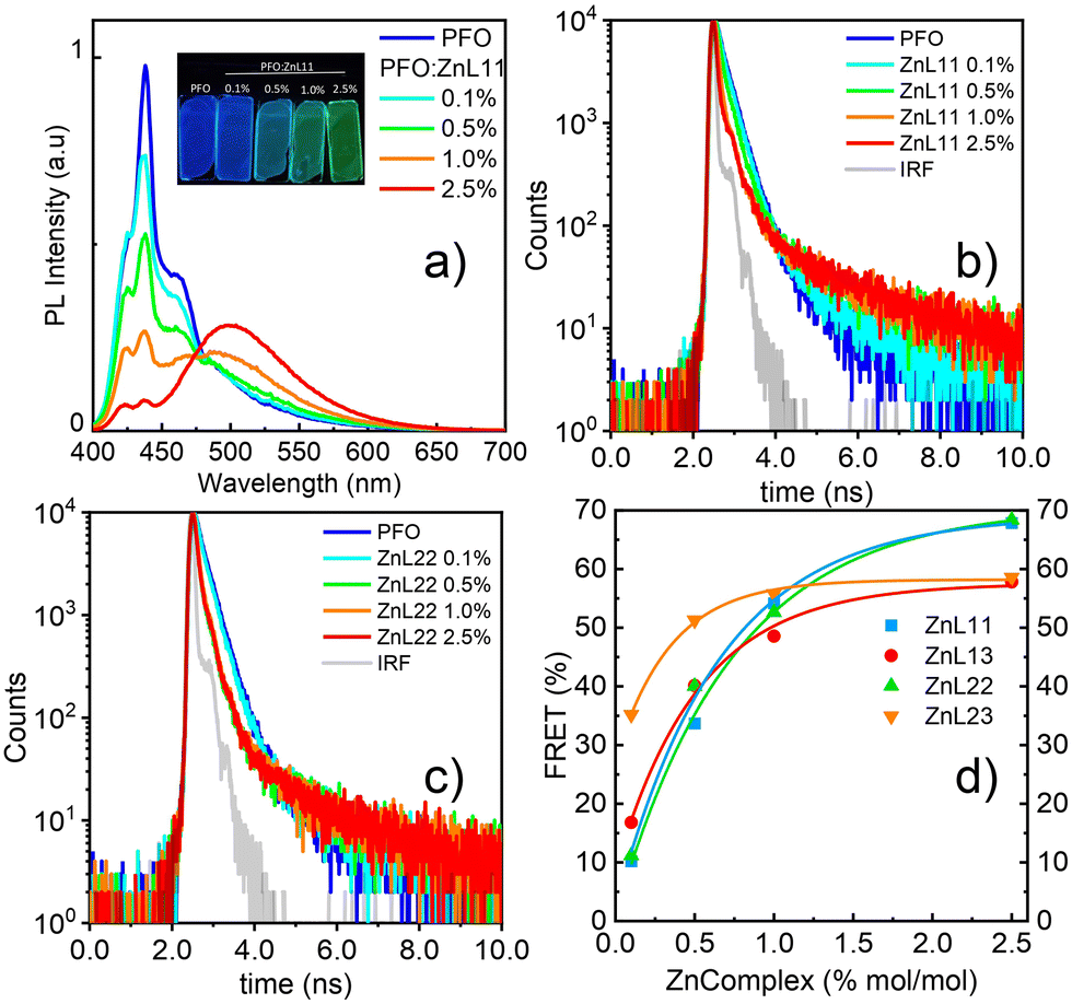 | ||
| Fig. 4 (a) Fluorescence spectra of the thin films (λexc = 375 nm). (b) and (c) Emission decays of ZnL11 and ZnL22 in different host–guest ratios (λexc = 370 nm; λem = 440 nm). (d) FRET efficiency (%) for all complexes. Data from ZnL22, ZnL13 and ZnL23 are summarized in the ESI† (see Fig. S17 and S18). | ||
Fig. 4(d) shows the plot of the equation data concerning the zinc(II) complex ratio. The proportion of 1% between the zinc(II) complexes in PFO is lower than that between the other complex, with a good FRET efficiency of 30–45%. The maximum efficiency occurred at 2.5% at 58–68%; however, there was a small difference in the efficiency at a 1.0% ratio. Table S1 (ESI†) summarizes the principal FRET data.
A critical factor in solution-processed OLEDs is the deposited film morphology. Typically, a loss of ordered molecular conformation leads to a high formation of intrinsic defects that are responsible for unbalanced electrical charge densities (via effect in electrical mobilities) and/or losses by recombination. These effects are not only related to the emitter itself, but also the host plays an important role.43,44 In this sense, an investigation based on confocal microscopy has shown the solubility of the zinc(II) complexes in the PFO host. The images were obtained using an argon laser at 458 nm (Fig. 5), where Zn(II) coordination compounds are preferentially excited. It is possible to observe the formation of aggregated structures, following an increase in the concentration of Zn(II)-homo and heteroligand compounds. As a general trend, Zn(II) coordination compounds based on L1 (ZnL11 and ZnL13) are more soluble than those based on L2 (ZnL22 and ZnL23), which form aggregates even at low concentrations (0.5%), leading to great changes in the morphology with increasing concentrations. The FRET efficiency is intricately linked with this observation, and, beyond a 1.0% ratio, all zinc(II) complexes saturate the host, being unfavorable to make a good film for a solution-processed OLED.
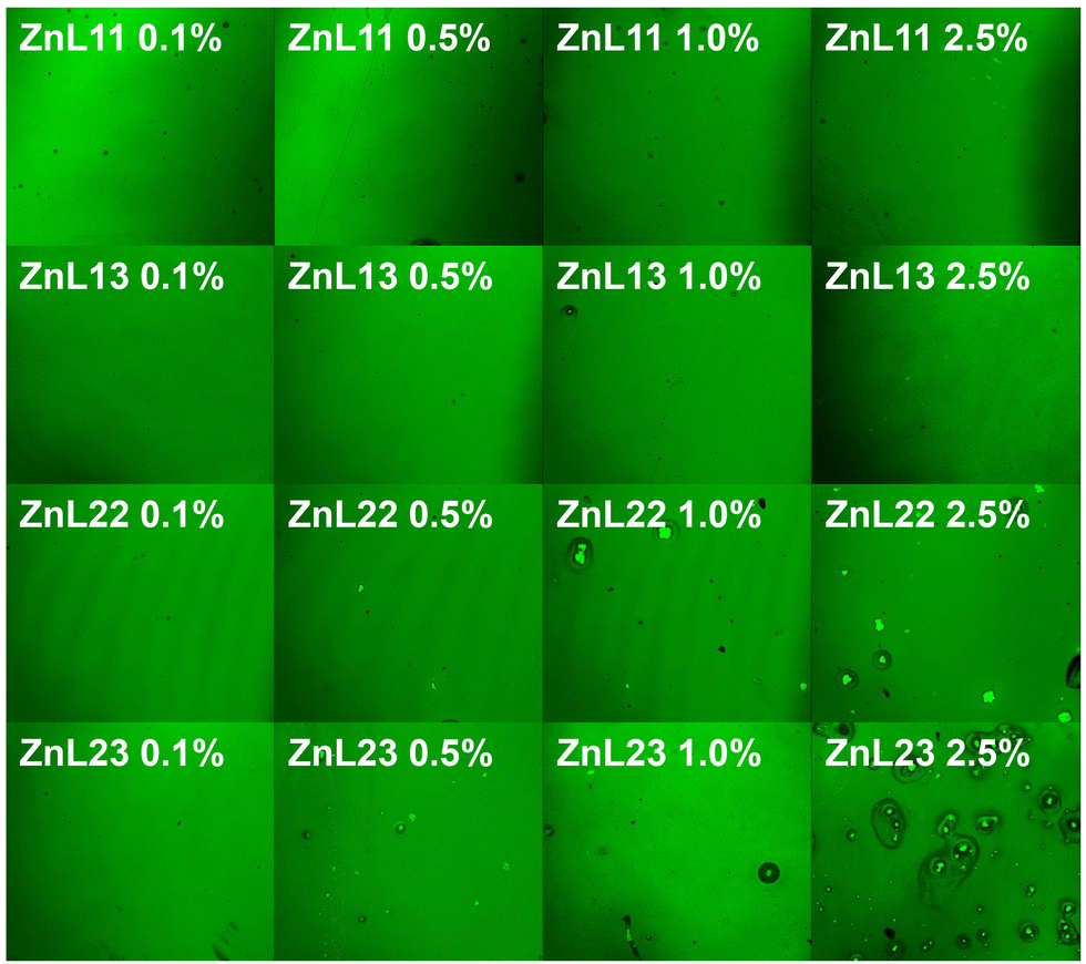 | ||
| Fig. 5 Confocal microscopy images of PFO:Zn(II) coordination compounds (λexc = at 458 nm). | ||
3.4. Solution-processed OLEDs’ optoelectronic properties
Considering the photophysical and morphological characterization of PFO-based zinc-homo (ZnL11 and ZnL22) and heteroligand (ZnL13 and ZnL23) complex composites, including energy transfer studies, we successfully employed them as emissive layers (EMLs) in solution-processed OLEDs in a proof of concept. Considering the FRET (Fig. 4(d)) efficiency and confocal microscopy images (Fig. 5), we chose a 1% (mol mol−1) concentration of each zinc(II) coordination compound in the PFO semiconducting polymer matrix because 1% concentration is the limit threshold for FRET efficiency and does not strongly disturb the thin-film morphology of the composite.The solution-processed OLEDs were assembled following the straightforward architecture previously described (scheme in Fig. 6(d)). PEDOT:PSS is a well-known metal-like conducting polymer blend that was used to optimize the ITO working function to −5.2 eV, while simultaneously acting as a hole injection layer.45 High-molecular weight PVK is a hole transporting polymer (μh ≈ 1 × 10⁻⁶ cm2 V−1 s−1) that has an EHOMO of −6.1 eV and an ELUMO of −1.2 eV,46 which enables PVK to be a good buffer layer, coupled with hole transport and electron blocking characteristics, confining the electrons on the interface with the emissive layer. TmPyPB was used as both an electron transport layer and a hole blocking layer (ELUMO of −2.7 eV and an EHOMO of −6.8 eV). The electron mobility of TmPyPB (μe ≈ 1 × 10⁻³ cm2 V−1 s−1)9 has the same magnitude as the PFO hole mobility,47 while the PFO electron mobility is very small; therefore, the combination of PVK and TmPyPB among the EML will guarantee the electrical balance of the proposed device. Finally, CalAl was thermally evaporated to optimize the cathode working function to −2.9 eV. Table 4 summarizes the optoelectronic characteristics of all the solution-processed OLEDs.
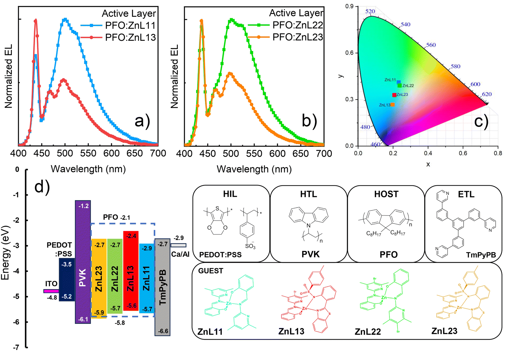 | ||
| Fig. 6 Electroluminescence spectra of ZnL11 (blue curve) and ZnL13 (red curve) (a) and ZnL22 (green curve) and ZnL23 (orange curve) (b) in the PFO matrix (1% mol mol−1), and the OLED chromaticity coordinate diagram CIE 1931 (c). Diagram level energy of each layer of the device and their chemical structures (d). | ||
| Optoelectronic properties | ZnL11 | ZnL13 | ZnL22 | ZnL23 |
|---|---|---|---|---|
| V on (V) | 12.5 | 9.5 | 9.0 | 8.5 |
| L max (cd m−2) | 533.1 | 351.7 | 668.2 | 536.8 |
| EQE (%) | 1.40 | 1.38 | 1.21 | 1.84 |
| EQEest (%) | 1.66 | 1.91 | 1.64 | 1.50 |
| EQE (100 cd m−2) | 1.25 | 1.30 | 1.06 | 1.55 |
| R off (%) | 11 | 6 | 12 | 16 |
| η C (cd A−1) | 2.08 | 1.58 | 1.81 | 2.11 |
| η P (lm W−1) | 0.38 | 0.30 | 0.37 | 0.49 |
| λ EL (nm)PFO; zinc(II) complex | 437; 501 | 437; 498 | 437; 502 | 437; 498 |
| V TFL (V) | 9.60 | 10.96 | 9.91 | 10.67 |
| N T (cm−3) | 3.18 × 10¹⁷ | 3.63 × 10¹⁷ | 3.28 × 10¹⁷ | 3.54 × 10¹⁷ |
| E T (meV) | 189 | 215 | 265 | 257 |
| μ eff (cm2 V−1 s−1) | 2.74 × 10⁻¹⁰ | 8.46 × 10⁻¹⁰ | 5.86 × 10⁻¹⁰ | 2.82 × 10⁻¹⁰ |
| μ SCLC (cm2 V−1 s−1) | 1.97 × 10⁻⁷ | 1.63 × 10⁻⁶ | 3.76 × 10⁻⁷ | 2.97 × 10⁻⁷ |
| θ 0 | 1.39 × 10⁻³ | 5.21 × 10⁻² | 1.56 × 10⁻³ | 9.51 × 10⁻⁴ |
| n 0 (cm−3) | 4.43 × 10¹⁴ | 1.90 × 10¹⁵ | 5.13 × 10¹⁴ | 3.37 × 10¹⁴ |
| μ TCLC (cm2 V−1 s−1) | 2.88 × 10⁻⁷ | 2.57 × 10⁻⁷ | 2.21 × 10⁻⁷ | 7.92 × 10⁻⁷ |
In general, the OLEDs’ electroluminescence (EL) spectra exhibit a combination of zinc(II) complex compounds and PFO matrix electroemission (Fig. 6(a) and (b)). A similar behavior was observed in the steady-state PL measurements. However, ZnL11 and ZnL22 compounds (λEL = 501 and 523 nm, and λEL = 502 and 525 nm, respectively) have shown more intense EL bands in contrast to the zinc(II)-heteroligand compounds (ZnL13 − λEL = 496 nm and 524 nm; ZnL23 − λEL = 498 nm and 525 nm), when compared to the PFO EL profile (λ(0-0)EL = 437 nm and λ(0-1)EL = 468 nm). These features lead to solution-processed OLEDs based on the zinc(II)-homoligands exhibiting greenish-blue emission, while zinc(II)-heteroligands to exhibit cyan-blue emission, according to the CIE1931 color diagram (Fig. 6(c)). Additionally, it is interesting to note that the OLED EL colors are very close to the center of the CIE diagram, which can enable the application of these devices in lighting technology (some specific lighting/decorative and signage applications), besides the usual display applications.
The observed behavior should be originated from several different factors, including, for instance, different materials solubility, energy level diagram compatibility, spectral overlap between PFO emission and zinc(II) complex absorption, complex PLQYs, device charge-carrier transport and recombination efficiency, electrical carrier injection balance and intrinsic defects, in which some of them can alter the recombination region in the organic layers of the device. From photophysical, FRET and confocal microscopy studies, no direct correlation could be observed when the EL features were contrasted, with the exception of the energy level alignment of each zinc(II) complex compound with the PFO matrix (Fig. 6(d)). To better understand the solution-processed PFO-based composite framework, we focused on the optoelectronic properties of the devices, in terms of their figures of merit, as well as charge-carrier transport characteristics under space-charge conditions (Fig. 7).
 | ||
| Fig. 7 Current density and brightness versus voltage curves (a), figures of merit versus brightness (roll-off) curves (b), and DC charge-carrier transport characteristics, according to J × V (log–log) curves, and current density versus voltage curve and the shallow-trap and deep-trap domain, and Child's Law (c) of the PFO-based zinc(II)-homo and heteroligand compound OLEDs. | ||
Fig. 7 presents the overall OLEDs’ figures of merit based on the zinc(II)-homo and heteroligand complexes in the PFO-matrix as EMLs, particularly current density and brightness versus voltage curves (Fig. 7(a)), external quantum, current and power efficiencies (EQE, ηc and ηp, respectively) versus brightness curves (Fig. 7(b)), and DC charge-carrier transport characteristics (Fig. 7(c)).
In general, the ZnL11 and ZnL22 compounds presented high brightness and driving voltage values in contrast to those of the ZnL13 and ZnL23 complexes, according to the sequence ZnL11 > ZnL22 > ZnL13 > ZnL23. On the other hand, the heteroligand compounds exhibited better performance parameters in terms of all the figures of merit, with ZnL23 > ZnL13 ≈ ZnL11 > ZnL22. From our data, zinc(II) complexes presents the following figures of merit: ZnL23 – Von = 8.5 V@Lmax = 536.8 cd m−2@EQEmax = 1.84%@ηCmax = 2.11 cd A−1@ηPmax = 0.49 lm W−1; ZnL13 − Von = 9.5 V@Lmax = 351.7 cd m−2@EQEmax = 1.38%@ηCmax = 1.58 cd A−1@ηPmax = 0.30 lm W−1; ZnL11 − Von = 12.5 V@Lmax = 533.1 cd m−2@EQEmax = 1.40%@ηCmax = 2.08 cd A−1@ηPmax = 0.38 lm W−1; and ZnL22 − Von = 9.0 V@Lmax = 668.2 cd m−2@EQEmax = 1.21%@ηCmax = 1.81 cd A−1@ηPmax = 0.37 lm W−1. Additionally, it is important to note that the obtained experimental EQE values of these solution-processed OLEDs are very close to the estimated ones, considering an approximation of the emissive layer PLQY. As for we know, these are the best results that have been achieved for zinc(II) salicylidene coordination compounds as emissive layers in electroluminescent diodes.19,26,48–51
Another important highlight that should be noted is that the OLEDs have a very low roll-off (Roff) of the EQE (Fig. 6(b)) as the brightness increases until L = 100 cd m−2, with ZnL13 − Roff = 6% < ZnL11@Roff = 11% < ZnL22@Roff = 12% < ZnL23@Roff = 16%. These behaviors could be directly linked to the fact that the ZnL13 and ZnL23 complexes can easily undergo charge transfer, as predicted by our DFT and TD-DFT simulations, which can facilitate the charge carriers’ transport toward the emissive layer; in contrast to zinc(II)-homoligand compounds, although, as previously mentioned, the molecular conformation in the active layer can induce intrinsic defects acting as traps for the electrical carriers. Despite, and at least for ZnL23, confocal microscopy images do not predict such a hypothesis, and the nanodomains of defects can exist.
To support such interpretations, we employed space-charge models in the DC current density versus voltages curves in shallow- (Mott–Gurney's law), deep- (Mark–Helfrich's law) and free-trap domains (Child's law) (Fig. 7(c); fit details on the ESI† Fig. S19–S22). It is well stated that space-charge models can be applied to obtain the charge-carrier mobilities when only one type of charge drifts along the device structure (electron- or hole-only diode).52 Despite this, an estimate of the global electrical mobility could be achieved by applying these models in an OLED, although it has ambipolar electrical injection, transport and recombination.15 At low driving voltages, during the shallow-trap filling process, the current density depends on a quadratic power with an applied voltage, also known as space-charge limited current (SCLC) behavior, as described by the Mott–Gurney equation53–55
 | (3) |
| μeff = μSCLCθ0 | (4) |
 | (5) |
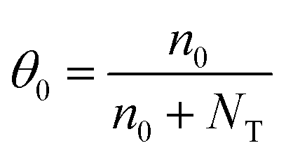
After the trap-filling process, the electrical mobilities of all the OLEDs increase by approximately 103 orders of magnitude, μSCLC(ZnL22) = 3.76 × 10⁻⁷ > μSCLC(ZnL23) 2.97 × 10⁻⁷ > μSCLC(ZnL11) 1.97 × 10⁻⁷ > μSCLC(ZnL13) = 1.63 × 10⁻⁷ cm2 V−1 s−1. Looking only for those values, in comparison with the shallow trap-filling electrical mobility ones, no absolute conclusive correlation with device figures of merit can be clearly observed. However, correlating OLED figures of merit with the θ0 parameter, it is clear that the density of trap-states and free-carriers impact, in our case, the electroemissive device efficiency loss (Roff), following the same trend (see Table 4). To obtain more insights about this, we determine the total density of trap-states (NT) of each kind of OLED by applying the trap-filled-limit voltage (VTFL) relationship:55
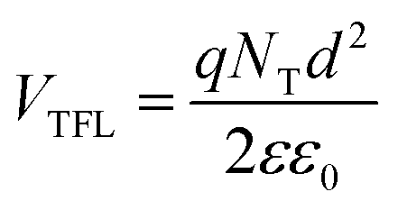 | (6) |
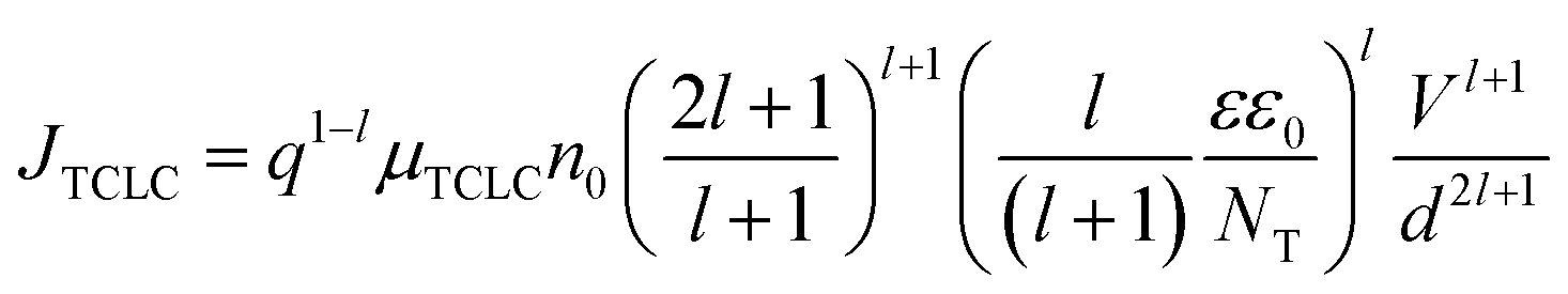 | (7) |
 , and μTCLC is the electrical mobility during the deep-trap filling. Considering these parameters and combining eqn (5) and (6), we can also estimate n0, and finally, determine μTCLC values for each kind of device.
Taking into account the obtained values for n0 and μTCLC (Table 4), we can observe some correlations with the OLEDs’ figures of merit: (i) n0 values follow the same trend with devices roll-off, as observed for θ0 values; and (ii) the electrical mobility during the deep-trap filling process of each OLED has shown a correlation with the devices figures of merit in terms of EQE, ηc and ηp. In other words, OLEDs with better optoelectronic properties exhibit high μTCLC values, while those with lower efficiency losses with brightness increments have high density of free-carriers. Although expected, our data seem to follow a well trend.
4. Conclusions
In summary, our study reports the synthesis and evaluation of four zinc(II) complexes with two newly synthesized and characterized ligands, aiming to modulate their photophysical and optoelectronic properties for applications in solution-processed OLEDs. Our approach involved the strategic combination of different ligands forming Zn(II) coordination compounds in a composite with PFO in 1% minimizing the morphological changes in the thin film. Theoretical predictions indicated that the L3 ligand possessed a higher bandgap energy compared to L1 and L2, resulting in a blue emission when complexed with zinc(II), thereby creating a wider energy gap relative to the green emission of ZnL11 and ZnL22. Consequently, while there were no significant alterations observed in the photophysical properties, slight modifications were noted in the optoelectronic characteristics of the complexes. Notably, our study revealed an increase in external quantum efficiency (EQE) associated with enhancements in electrical mobility and trap-density parameters. This underscores the effectiveness of our novel approach in utilizing zinc(II) complexes with different ligands to fine tune the optoelectronic properties, thus offering a new perspective on their application in OLEDs. In essence, our findings present a promising framework for the rational design of zinc(II) complexes, wherein the insertion of distinct ligands can effectively tailor optoelectronic properties while maintaining morphological integrity. This approach opens new possibilities for the development of solution-processed OLEDs with improved performance and versatility, contributing to the advancement of lighting technologies and beyond.Author contributions
E. S. M.: conceptualization, formal analysis, investigation, writing – original draft, and writing – review and editing; L. G. T. A. D.: conceptualization, investigation, writing – original draft, and writing – review and editing; F. S. R.: supervision, writing – original draft, and writing – review and editing; J. C. G.: supervision, conceptualization, formal analysis, investigation, writing – original draft, and writing – review and editing. L. F. R. P.: funding acquisition, project administration, resources, software assembly, and writing – review and editing. T. D. Z. A.: funding acquisition, project administration, resources, and writing – review and editing.Data availability
The data supporting this article have been included as part of the ESI.†Conflicts of interest
The authors declare no conflicts of interest.Acknowledgements
E. S. M., J. C. G. and L. F. R. P. acknowledge the Institute for Nanostructures, Nanomodeling, and Nanofabrication (i3N) associated laboratory of the Portuguese Foundation for Science and Technology (FCT) (UIDB/50025/2020 & UIDP/50025/2020). J. C. G. also thanks FCT/i3N/UA for the individual CEEC grant (2021.02056.CEECIND) to E. S. M., L. G. T. A. D., F. S. R. and T. D. Z. A. We are thankful for financial support from CNPq (305954/2019-9), FAPESP (2013/16245-2 and 2013/07375-0), FAEPEX, and INEO (MCTI/CNPq). This research was supported in part by the Coordenação de Aperfeiçoamento de Pessoal de Nível Superior – Brasil (CAPES) – Finance Code 001.References
- J. Y. Woo, M. Park, S. Jeong, Y. Kim, B. Kim, T. Lee and T. Han, Adv. Mater., 2023, 35, 2207454 CrossRef CAS PubMed.
- X. Ban, F. Chen, J. Pan, Y. Liu, A. Zhu, W. Jiang and Y. Sun, Chem. – Eur. J., 2020, 26, 3090–3102 CrossRef CAS PubMed.
- C. Amruth, D. K. Dubey, M. Pahlevani and G. C. Welch, Adv. Mater. Technol., 2021, 6, 2100264 CrossRef.
- Q.-S. Tian, W.-S. Shen, Y.-J. Yu, X.-Q. Wang, J.-H. Cai, Y. Hu, Z.-Q. Jiang, J.-S. Huang and L.-S. Liao, Org. Electron., 2022, 100, 1566–1599 CrossRef.
- C. Kant, S. Mahmood and M. Katiyar, Adv. Mater. Technol., 2023, 8, 2201514 CrossRef CAS.
- F. Teixeira, J. C. Germino and L. Pereira, Appl. Sci., 2023, 13, 12020 CrossRef CAS.
- M. Kumar and L. Pereira, J. Visualized Exp., 2022, e61071 Search PubMed.
- M. Kumar and L. Pereira, ACS Omega, 2020, 5, 2196–2204 CrossRef CAS PubMed.
- M. Kumar and L. Pereira, Nanomaterials, 2020, 10, 101 CrossRef CAS PubMed.
- M. Kumar, M. Chapran, G. Wiosna-Salyga, P. Sleczkowski, B. Luszczynska and L. Pereira, J. Phys. Chem. C, 2020, 124, 21935–21947 CrossRef CAS.
- E. S. Hellerich, J. J. Intemann, M. Cai, R. Liu, M. D. Ewan, B. C. Tlach, M. Jeffries-El, R. Shinar and J. Shinar, J. Mater. Chem., 2013, 1, 5191–5199 CAS.
- K. Kishore Kesavan, J. Jayakumar, M. Lee, C. Hexin, S. Sudheendran Swayamprabha, D. Kumar Dubey, F. C. Tung, C. W. Wang and J. H. Jou, Chem. Eng. J., 2022, 435, 134879 CrossRef CAS.
- L. Wang, J. Miao, Y. Zhang, C. Wu, H. Huang, X. Wang and C. Yang, Adv. Mater., 2023, 35, 2303066 CrossRef CAS PubMed.
- L. Zhu, C. Sha, A. Lv, W. Xie, K. Shen, Y. Chen, G. Xie, H. Ma, H. Li and X. C. Hang, Inorg. Chem., 2022, 61, 10402–10409 CrossRef CAS PubMed.
- J. C. Germino, L. G. T. A. Duarte, R. A. Mendes, M. M. Faleiros, A. de Morais, J. N. de Freitas, L. Pereira and T. D. Z. Atvars, Nanomaterials, 2022, 12, 2497 CrossRef CAS PubMed.
- J. C. Germino, J. N. de Freitas, R. A. Domingues, F. J. Quites, M. M. Faleiros and T. D. Z. Atvars, Synth. Met., 2018, 241, 7–16 CrossRef CAS.
- L. G. T. A. Duarte, J. C. Germino, R. A. Mendes, J. F. Berbigier, M. M. Faleiros, F. S. Rodembusch and T. D. Z. Atvars, Dyes Pigm., 2019, 171, 107671 CrossRef CAS.
- L. G. T. A. Duarte, J. C. Germino, J. F. Berbigier, C. A. Barboza, M. M. Faleiros, D. De Alencar Simoni, M. T. Galante, M. S. De Holanda, F. S. Rodembusch and T. D. Z. Atvars, Phys. Chem. Chem. Phys., 2019, 21, 1172–1182 RSC.
- L. G. T. A. Duarte, J. C. Germino, R. A. Mendes, J. F. Berbigier, K. S. Moreira, M. M. Faleiros, J. N. De Freitas, T. A. L. Burgo, F. S. Rodembusch and T. D. Z. Atvars, J. Phys. Chem. C, 2020, 124, 21036–21046 CrossRef CAS.
- M. Chen, Y.-P. Xiao, Y. Wang, W. Cheng, J. Zhang, P. Wang, S.-H. Ye and B.-H. Tong, Inorg. Chim. Acta, 2021, 516, 120100 CrossRef CAS.
- R. G. Alabau, B. Eguillor, J. Esler, M. A. Esteruelas, M. Oliván, E. Oñate, J. Y. Tsai and C. Xia, Organometallics, 2014, 33, 5582–5596 CrossRef CAS.
- G. Santos, F. J. Fonseca, A. M. de Andrade, T. Monteiro and L. F. R. Pereira, Phys. Status Solidi A, 2008, 8, 2057–2060 CrossRef.
- S. K. Mizoguchi, G. Santos, A. M. Andrade, F. J. Fonseca, L. Pereira and N. Y. Murakami Iha, Synth. Met., 2011, 161, 1972–1975 CrossRef CAS.
- C. Bizzarri, E. Spuling, D. M. Knoll, D. Volz and S. Bräse, Coord. Chem. Rev., 2018, 373, 49–82 CrossRef CAS.
- A. N. Gusev, M. A. Kiskin, E. V. Braga, M. A. Kryukova, G. V. Baryshnikov, N. N. Karaush-Karmazin, V. A. Minaeva, B. F. Minaev, K. Ivaniuk, P. Stakhira, H. Ågren and W. Linert, ACS Appl. Electron. Mater., 2021, 3, 3436–3444 CrossRef CAS.
- H. Xu, Z. F. Xu, Z. Y. Yue, P. F. Yan, B. Wang, L. W. Jia, G. M. Li, W. Bin Sun and J. W. Zhang, J. Phys. Chem. C, 2008, 112, 15517–15525 CrossRef CAS.
- A. N. Gusev, M. A. Kiskin, E. V. Braga, M. Chapran, G. Wiosna-Salyga, G. V. Baryshnikov, V. A. Minaeva, B. F. Minaev, K. Ivaniuk, P. Stakhira, H. Ågren and W. Linert, J. Phys. Chem. C, 2019, 123, 11850–11859 CrossRef CAS.
- H. W. Tseng, J. Q. Liu, Y. A. Chen, C. M. Chao, K. M. Liu, C. L. Chen, T. C. Lin, C. H. Hung, Y. L. Chou, T. C. Lin, T. L. Wang and P. T. Chou, J. Phys. Chem. Lett., 2015, 6, 1477–1486 CrossRef CAS PubMed.
- E. S. Moraes, L. G. Teixeira Alves Duarte, J. C. Germino and T. D. Z. Atvars, J. Phys. Chem. C, 2020, 124, 22406–22415 CrossRef CAS.
- G. M. Sheldrick, Acta Crystallogr., Sect. A: Found. Crystallogr., 2008, 64, 112–122 CrossRef CAS PubMed.
- G. M. Sheldrick, Acta Crystallogr., Sect. C: Struct. Chem., 2015, 71, 3–8 Search PubMed.
- J. P. Perdew, K. Burke and M. Ernzerhof, Am. Phys. Soc., 1996, 77, 3865–3868 CAS.
- F. Weigend, Phys. Chem. Chem. Phys., 2006, 8, 1057–1065 RSC.
- R. Izsák and F. Neese, J. Chem. Phys., 2011, 135, 144105 CrossRef PubMed.
- F. Neese, Wiley Interdiscip. Rev.: Comput. Mol. Sci., 2022, 12, 1–15 Search PubMed.
- F. Neese, F. Wennmohs, U. Becker and C. Riplinger, J. Chem. Phys., 2020, 152, 224108 CrossRef CAS PubMed.
- A. R. Allouche, J. Comput. Chem., 2011, 32, 174–182 CrossRef CAS PubMed.
- R. López, Adv. Math., 2014, 262, 476–483 CrossRef.
- M. Enamullah, M. A. Quddus, M. A. Halim, M. K. Islam, V. Vasylyeva and C. Janiak, Inorg. Chim. Acta, 2015, 427, 103–111 CrossRef CAS.
- X.-F. Zhang, I. Zhang and L. Liu, Photochem. Photobiol., 2010, 86, 492–498 CrossRef CAS PubMed.
- H. J. Eggimann, F. Le Roux and L. M. Herz, J. Phys. Chem. Lett., 2019, 10, 1729–1736 CrossRef CAS PubMed.
- D. L. Andrews and A. A. Demidov, Resonance Energy Transfer, Wiley, 1999, vol. 1 Search PubMed.
- F. Samaeifar, H. Yu, T. Davidson-Hall, M. Sadeghianlemraski, D. S. Chung and H. Aziz, J. Phys. Chem. C, 2021, 125, 20094–20103 CrossRef CAS.
- M. Kumar and L. Pereira, Nanomater., 2019, 9, 1307 CrossRef CAS PubMed.
- W. Kim, N. Kim, J. K. Kim, I. Park, Y. S. Choi, D. H. Wang, H. Chae and J. H. Park, ChemSusChem, 2013, 6, 1070–1075 CrossRef CAS PubMed.
- J. Jeong, J. Lee, H. Lee, G. Hyun, S. Park, Y. Yi, S. W. Cho and H. Lee, Chem. Phys. Lett., 2018, 706, 317–322 CrossRef CAS.
- A. Babel and S. A. Jenekhe, Macromolecules, 2003, 36, 7759–7764 CrossRef CAS.
- F. Dumur, Synth. Met., 2014, 195, 241–251 CrossRef CAS.
- F. Dumur, L. Beouch, M.-A. Tehfe, E. Contal, M. Lepeltier, G. Wantz, B. Graff, F. Goubard, C. R. Mayer, J. Lalevée and D. Gigmes, Thin Solid Films, 2014, 564, 351–360 CrossRef CAS.
- T. D. Z. Germino, J. C. Quites, F. J. Faria, G. C. Ramos, R. J. Atvars, J. C. Germino, F. J. Quites, G. C. Faria, R. J. Ramos, T. D. Z. Atvars, T. D. Z. Germino, J. C. Quites, F. J. Faria, G. C. Ramos and R. J. Atvars, J. Braz. Chem. Soc., 2016, 27, 295–302 Search PubMed.
- J. C. Germino, J. N. de Freitas, R. A. Domingues, F. J. Quites, M. M. Faleiros and T. D. Z. Atvars, Synth. Met., 2018, 241, 7–16 CrossRef CAS.
- M. Pope and S. E. Charles, Electronic processes in organic crystals and polymers, Oxford University Press, New York, 2nd edn, 1999 Search PubMed.
- N. F. Mott and R. W. Gurney, Electronic Processes in Ionic Crystals, Oxford University Press, London, UK, 2nd edn, 1948 Search PubMed.
- A. M. Stoneham, Phys. Bull., 1970, 21, 558 CrossRef.
- L. Pereira, Organic Light Emitting Diodes, Jenny Stanford Publishing, 2012 Search PubMed.
- P. Mark and W. Helfrich, J. Appl. Phys., 1962, 33, 205–215 CrossRef CAS.
Footnotes |
| † Electronic supplementary information (ESI) available. CCDC 2210785, 2210790 and 2210791. For ESI and crystallographic data in CIF or other electronic format see DOI: https://doi.org/10.1039/d4ma00581c |
| ‡ These authors contributed equally to this work. |
| This journal is © The Royal Society of Chemistry 2024 |