DOI:
10.1039/D4MA01011F
(Paper)
Mater. Adv., 2024,
5, 9823-9837
Bismuth and tellurium co-doping: a route to improve thermoelectric efficiency in InSe polycrystals
Received
8th October 2024
, Accepted 10th November 2024
First published on 26th November 2024
Abstract
Indium selenide (InSe), a layered chalcogenide material, has gained substantial scientific interest as a thermoelectric material due to its intrinsic low thermal conductivity. However, its intrinsic carrier concentration is notably minimal (∼1014 cm−3) due to a significant bandgap of 1.3 eV limiting its thermoelectric efficiency. Therefore, to optimize InSe-based materials for thermoelectric applications, it is essential to increase the carrier concentration through precise doping methodologies. In this study, co-doping at both the anion and cation sites of InSe was achieved by introducing Bi to the In site and Te to the Se site. The impact of this co-doping on the thermoelectric performance of InSe-based materials was thoroughly investigated. The increase in carrier concentration due to the electron-donating nature of Bi significantly enhanced the electrical transport properties and the Seebeck coefficient (S) experienced a minor reduction, and the incorporation of Bi atoms resulted in a substantial improvement in the power factor (PF) across the temperature range. Among all the samples studied, In0.96Bi0.04Se0.97Te0.03 exhibited the highest PF throughout the temperature range. The dopants Bi/Te acted as an effective phonon scattering center, reducing lattice thermal conductivity. The synergistic effect of cation–anion co-doping resulted in a maximum ZT of ∼0.13 at 630 K in the In0.96Bi0.04Se0.97Te0.03 sample, which is nearly 11 times higher compared to the pristine sample. Considering these findings, Bi–Te co-doped InSe emerged as a highly promising material for thermoelectric applications.
1. Introduction
The current global energy crisis and ecological problems due to the growing population, industrial production, and exhaustion of non-renewable energy sources like coal, natural gas, and petroleum are causing widespread suffering and preventing humankind from progressing further.1,2 The global increase in energy consumption has drawn considerable research attention toward novel renewable energy conversion technologies based on clean energy sources. Thermoelectrics (TE) is a key technology in the current renewable energy landscape and has shown great promise for producing electricity from waste heat.3 But by using conventional semiconductor-based systems, solar energy devices, for instance, can only produce electricity in response to 50–60% of the sun's radiation that falls within the visible and ultraviolet portions of the spectrum. In contrast, thermoelectric devices can convert a large portion of the sun's remaining 40–50% of radiation, primarily infrared, into electricity. Thus, combining photovoltaic and thermoelectric devices would greatly expand the range of solar radiation that is available for energy conversion.4 So, in this work, we discuss the thermoelectric aspect.
Thermoelectric materials have drawn a great deal of interest because they facilitate waste heat recovery by converting heat into electricity. Thermoelectric materials are safe for the environment and a potential candidate to help with overall global energy management with benefits like having no moving parts, requiring little maintenance, and operating for a longer period over a wide temperature range.5 Due to its reliability and simplicity, thermoelectric technology has been widely used in a variety of industries, including deep space missions, refrigeration, and electronic cooling.2 The energy conversion efficiency, the figure of merit (ZT) of thermoelectric devices, serves as a measure of their effectiveness. It is defined as ZT = S2σ/(κL + κe) where σ stands for electrical conductivity, S is the Seebeck coefficient, κe stands for electronic thermal conductivity, κL is the lattice thermal conductivity, and T is the absolute temperature. A ZT greater than 1 is generally required for commercial applications, and the main barrier to using TE devices in a variety of applications is their low efficiency, which is difficult to improve. High Seebeck coefficient and electrical conductivity are necessary for a good ZT value, but thermal conductivity must be low. However, the Wiedemann–Franz law (κe = LσT) states that high electronic thermal conductivity (κe) is equivalent to high electrical conductivity (σ).6 All other thermoelectric parameters for a given material, aside from lattice thermal conductivity, depend on carrier concentration. To fully utilize a material's potential for a thermoelectric device, an optimized carrier concentration, typically in the range of 1017 to 1021 cm−3, is desirable, as it balances electrical conductivity and the Seebeck coefficient to maximize ZT. Several strategies, including doping,7 alloying,8 and composites,9 are suggested to increase the TE efficiency. By doping, the electrical conductivity can be significantly improved. However, the Seebeck coefficient and the electrical conductivity of the compounds are inversely related to the carrier concentration. Due to the dopant's solubility restriction, balance control of electrical conductivity, Seebeck coefficient, and thermal conductivity are essential for a high figure of merit through single doping. Compared to single doping, dual doping considerably enhances the thermoelectric properties.10
Recent developments in thermoelectric research have concentrated on creating inexpensive, high-performance materials using elements that are abundant in earth and are environmentally friendly. For instance, recent reports of high ZT values for chemically straightforward binary compounds11 and numerous semiconducting chalcogenides have undergone extensive research for thermoelectric use. The thermoelectric performance in sustainable energy is greatly influenced by metal chalcogenide materials (PbTe,12 PbSe,13 SnTe,14 SnSe,15 and InTe16). These chalcogenides can increase the thermoelectric features of the devices by converting thermal energy to electrical energy.17 However, despite lead chalcogenides being well-known for their thermoelectric properties and higher ZT values, their use is limited by lead toxicity and environmental concerns, which pose significant challenges for large-scale applications.18 In contrast, InSe offers several advantages, such as ambient stability, a direct band gap in the visible regime, and active electronic edge states.4 Indium mono selenide is a semiconductor belonging to a III–VI layered compound19 with a direct band gap of 1.3 eV at room temperature20 and Se–In–In–Se atoms are stacked in layers to form InSe, which has covalently bonded layers with weak van der Waals forces between its quadruple layers.21 Indium selenide could be formed in hexagonal (β-InSe) and rhombohedral (γ-InSe) structures with space groups of P63/mmc and R3m, respectively.22 Even though numerous research groups have examined the structural, electronic, and optical characteristics of InSe, the results are inconsistent because most of the measurements were made on multiphase crystals. Due to the coexistence of several phases, including InSe,23 In2Se3,24 In4Se3,25 and In6Se7,26 and the substantial difference in vapor pressure between In and Se, it is difficult to prepare single crystalline InSe.27 Because of its outstanding tunable electrical properties as well as low thermal conductivity, InSe is a promising thermoelectric material. A low thermal conductivity range of 0.37 to 1.2 W m−1 K−1 has been reported for InSe.28 However, InSe exhibits a comparatively wide band gap, resulting in a low intrinsic carrier concentration of approximately 1014 cm−3.29 Consequently, numerous attempts have been made to enhance InSe's thermoelectric performance through the implementation of various approaches. For example, Raad Haleoot et al. conducted a theoretical investigation on the thermoelectric properties of both InSe and Bi-doped InSe. Doping with Bi in the InSe matrix results in a 50% decrease in the κL value of β-InSe0.75Bi0.25 compared to β-InSe at 300 K. This resulted in an increase in the ZT value to 0.65 at 800 K.23 Ji-il Kim et al. investigated the electrical and thermal transport properties of InSe polycrystalline samples doped with 7% S or Te. Anion substitutions improved the electrical conductivity of InSe, with Te-doped InSe showing a greater improvement due to its smaller bandgap. Doping significantly reduced thermal conductivity due to increased point defect phonon scattering. The ZT increased by 62% and 230%, reaching a maximum of 0.13 and 0.28, respectively, at 735 K for InSe0.93S0.07 and InSe0.93Te0.07.30 Jeon et al. reported that doping Si and Te to InSe will enhance the ZT to about 2 times greater than that of InSe in the In0.9Si0.1Se0.9Te0.07 composition.31
Inspired by the results from the aforementioned literature review, we adopted a co-doping approach to enhance the thermoelectric performance of InSe. The literature shows that doping InSe with Bi and Te can significantly improve the electrical properties while reducing thermal conductivity. This has prompted us to investigate the combined effects of these two dopants, as we seek to understand their synergistic interaction and the potential to further optimize the thermoelectric performance of InSe. In this study, the solid-state metathesis route is utilized to synthesize In1−xBixSe0.97Te0.03 (x = 0, 0.02, 0.04, 0.06) samples by doping Bi at the In site and Te at the Se site with varying Bi concentrations in the matrix. Te and heavy Bi atom selection is expected to enhance the electrical characteristics and lower the lattice thermal conductivity. As expected, point defect scattering caused by the co-doping decreased the thermal conductivity, and an increase in σ was found with a slight decrement in S. As a result, the sample doped with 4% Bi has shown high PF and ZT values of 67.2 μW m−1 K−2 and 0.12 at 630 K, respectively. The novelty of this work lies in the synergistic effect of Bi and Te co-doping, which significantly enhances the thermoelectric performance of InSe by optimizing carrier concentration and reducing thermal conductivity, positioning Bi–Te co-doped InSe as a superior thermoelectric material. Future work should focus on optimizing the doping concentrations, exploring other dopant combinations, and investigating long-term stability and scalability for practical applications.
2. Experimental procedure
2.1 Sample synthesis
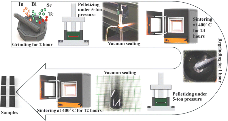
A familiar solid-state reaction technique was used to synthesize InSe and co-doped InSe (In1−xBixSe0.97Te0.03) polycrystalline samples (x = 0, 0.02, 0.04, and 0.06). During synthesis, Bi and Te atoms are intended to substitute In and Se atoms within the InSe lattice, ensuring substitutional doping. For synthesis purposes, stoichiometric amounts of precursors like In (99.9% Alfa Aesar, Hyderabad), Bi, Se, and Te (99.999% Molychem, Mumbai, India) powders were used. Four grams of material for each composition using a common atomic weight percentage calculation was used. Then precursors were mixed in an appropriate stoichiometric ratio and hand-ground in an agate mortar for two hours. Using a hydraulic press with a pressure of 5 tons, the fine powder was compressed into pellets and sealed in a quartz tube with a 10−4 torr vacuum. For 24 hours, the pellet samples were sintered at 400 °C with natural cooling. The grinding procedure was repeated for one hour to achieve the ideal homogeneity in the compound. This powder was again pelletized and heated to 400 °C for 12 hours. Fig. 1 illustrates a schematic of the preparation of InSe and co-doped InSe polycrystalline samples.
 |
| | Fig. 1 A schematic depiction of sample synthesis using a solid-state metathesis pathway. | |
2.2 Characterization techniques
Powder X-ray diffraction (XRD) was carried out on the synthesized samples using a Rigaku Ultima IV diffractometer equipped with a CuKα (λ = 1.54 Å) radiation source, and the patterns of XRD were identified with a scan rate of 2° min−1 in the 20°–80° range with a step size of 0.02° to validate the structure, purity, crystallinity, dominant phase, and compound formation. For Rietveld refinement, the “EXPO 2014 software” was utilized. The surface morphological features of the samples were investigated by employing a field emission scanning electron microscope (Carl Zeiss Sigma) with a particle size range of 1 μm and a magnification of 40 KX. The chemical composition of the grown samples was determined using energy dispersive electron X-ray analysis (EVO MA18 and Oxford EDS (X-act)). A Vickers microhardness tester (MMTX3/MMTX7 Matsuzawa CO. Ltd) was used to measure the samples' hardness. The density of the synthesized samples was calculated using the CONTECH CAS – 234 density measurement system. The Van der Pauw method was adopted to determine carrier concentration and mobility at room temperature using a “Keithley meter 6220” at a magnetic field of 0.6 T and an electric current of 50 mA. The pellets were polished to a parallelepiped shape with dimensions of roughly (2 × 4 × 10) mm3 to measure the electrical resistivity (σ) and Seebeck coefficient (S) simultaneously. Measurements were performed between 300–663 K in an argon atmosphere using a ZEM 3 (ADVANCE RIKO). For S and σ, the error margin is ∼5% and ∼3%, respectively. An LFA 467 HT instrument was used to measure the specific heat capacity (Cp) and thermal diffusivity (D) of the pellets, which had a diameter of approximately 12.7 mm and a thickness of approximately 2.0 mm. The measurements were taken entirely between the 300–663 K range. The error margin for thermal conductivity (κ) is ∼5%.
3. Results and discussion
3.1 Powder X-ray diffraction: structural investigation
Fig. 2a shows the XRD peak patterns collected for InSe and doped InSe samples, showing that the material is polycrystalline. All diffraction peaks agree with the standard JCPDS card no. 34–1431 data. The patterns were indexed, and their peaks were identified for the hexagonal crystal system with space group P63/mmc and sublayers in the form of a Se–In–In–Se pattern.32 It is verified that all the prepared samples show a single phase and are formed as intended because there isn't another peak within the XRD measurement limit. The XRD results show an intense peak at a diffraction angle of 21.42° that corresponds to the (0 0 4) plane. Refer to Fig. 2b for an enlarged view of the (0 0 4) diffraction peak. As a result of Bi atoms substituting In sites in the lattice, it is possible to observe a left shift (lower angle) for the Bi/Te codoped samples, which indicates a lattice expansion in the 2%, 4%, and 6% Bi-doped samples. This confirms that Bi atoms occupy substitutional sites in the InSe matrix, replacing In atoms within the crystal structure. Fig. 2c shows the change in lattice parameters a and c effectively with the dopant contents, which is tabulated in Table 1. In accordance with the slightly larger atomic radius of Bi3+ (130 pm) than In2+ (80 pm), the lattice parameter increased as the Bi content increased. The changes in lattice parameters indicate that substitutional doping effectively confirmed the incorporation of the dopant atom into the InSe lattice, which is consistent with previous reports.30 Because the dopants' atomic radii are slightly different from those of the parent atoms, the matrix is strained. So after doping, the strain is generated, and the results are listed in Table 1.
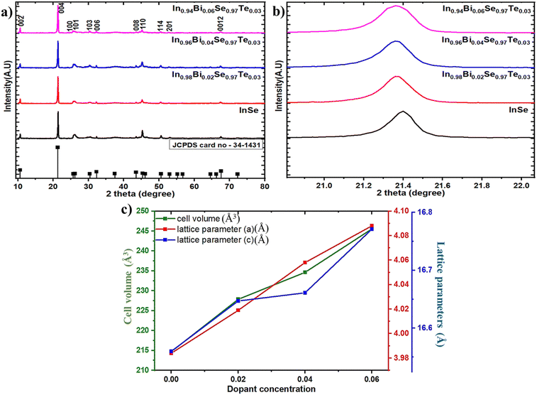 |
| | Fig. 2 (a) Powder XRD peak, (b) shift in the XRD peak pattern, and (c) lattice parameter and cell volume variation of In1−xBixSe0.97Te0.03 (x = 0, 0.02, 0.04, 0.06) polycrystal samples. | |
Table 1 Powder XRD data interpretation of pure and codoped InSe polycrystalline samples
| Sample |
InSe |
In0.98Bi0.02Se0.97Te0.03 |
In0.96Bi0.04Se0.97Te0.03 |
In0.94Bi0.06Se0.97Te0.03 |
|
R
p
|
14.59 |
16.23 |
15.88 |
17.12 |
|
R
wp
|
19.17 |
21.01 |
20.90 |
22.44 |
|
R
ep
|
8.47 |
8.18 |
8.45 |
7.86 |
|
χ
2
|
2.1 |
1.6 |
2.1 |
1.8 |
| Crystallite size (D) (nm) |
WH method |
76 ± 2 |
69 ± 4 |
55 ± 3 |
47± 6 |
| Scherrer method |
65 ± 2 |
59 ± 3 |
53 ± 3 |
49 ± 2 |
|
a = b (Å) |
3.984 |
4.019 |
4.058 |
4.088 |
|
c (Å) |
16.560 |
16.647 |
16.661 |
16.771 |
| Cell volume (Å3) |
214.70 |
227.85 |
234.63 |
245.53 |
| Strain (ε) 10−4 |
15.4 ± 2.8 |
19.4 ± 2.8 |
20.9 ± 3.4 |
24.1 ± 2.8 |
| Density (g cm−3) |
5.82 |
5.86 |
5.88 |
5.90 |
Fig. 3 shows the XRD patterns fitted with the Rietveld refinement using “EXPO 2014” software. Table 1 depicts the values of Rp (profile factor), Rwp (weighted profile factor), Rep (expected profile factor), χ2 (goodness of fit), lattice parameters, lattice strain, cell volume, density, and crystallite size of the prepared samples.
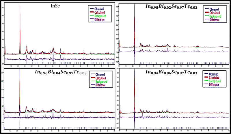 |
| | Fig. 3 Rietvield refinement XRD plots of In1−xBixSe0.97Te0.03 (x = 0, 0.02, 0.04, 0.06) polycrystal samples. | |
An array of methods was used to estimate the strain (ε) and crystallite size (D), including the Scherrer and Williamson–Hall methods. The Scherrer equation is provided by ref. 33,
| |  | (1) |
to calculate the average crystallite size (
D), where
β – FWHM
λ – wavelength of X-ray,
θ – Braggs diffraction angle. According to
eqn (1), the average crystallite size ranged between 49 and 65 nm, as shown in
Table 1.
The following Williamson–Hall formula is used to calculate the crystallite size (D) and the lattice strain (ε) is given by ref. 20,
| |  | (2) |
The plotting of
β![[thin space (1/6-em)]](https://www.rsc.org/images/entities/char_2009.gif)
cos
![[thin space (1/6-em)]](https://www.rsc.org/images/entities/char_2009.gif) θ
θ on the
y-axis
vs. 4
![[thin space (1/6-em)]](https://www.rsc.org/images/entities/char_2009.gif)
sin
![[thin space (1/6-em)]](https://www.rsc.org/images/entities/char_2009.gif) θ
θ on the
x-axis enables the line (
y =
mx +
c) to be fitted to the data.
Fig. 4 shows the experiment data as well as the fitted graphs. The strain values were calculated using the line's slope (
ε =
m), and the crystallite size was determined using the line's intercept (
D =
kλ/
c). The crystallite size is found to typically range between 47 and 76 nm using the WH technique. Impurities known as dopants can function as point defects in polycrystalline materials, increasing the strain on the lattice. Dopants can modify the lattice parameters in addition to raising strain.
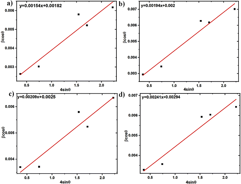 |
| | Fig. 4 WH plots of (a) InSe, (b) In0.98Bi0.02Se0.97Te0.03, (c) In0.96Bi0.04Se0.97Te0.03 and (d) In0.94Bi0.06Se0.97Te0.03 samples. | |
3.2 Mechanical hardness
The appropriateness of a crystalline surface for a particular application depends on the mechanical properties of a grown crystal.34 Mechanical strength is a well-known and important production indicator for thermoelectric modules. For these materials to be used in thermoelectric systems, their mechanical qualities must be improved.35 A Vicker's hardness tester with a diamond micro indenter is used to measure the hardness of the prepared samples.36 The load and dwell times are set to 200 g and 15 seconds, respectively. This test is non-destructive and will provide quantitative data regarding the materials' strength rapidly.37Fig. 5 shows the hardness values of the In1−xBixSe0.97Te0.03 (x = 0, 0.02, 0.04, 0.06) polycrystal samples. The x = 6% doped sample shows much higher hardness (1.3 times) than the pristine InSe sample. The hardness of the InSe sample is 36 (±10%) HV, while the hardness of In0.94Bi0.06Se0.97Te0.03 is found to be 47 (±10%) HV. The results indicate that the dopants considerably increase hardness. An increase in dopant concentration may improve the microhardness of the InSe matrix by filling the intergranular space and strengthening the material.38 In addition to the increase in microhardness, the phenomenon can also be explained by the maximum elastic interaction energy between the dislocation and dopant atoms. The parameter for elastic interaction (ξ) can be determined by using,39| |  | (3) |
where the dopant atom's covalent radius represented by r1, is 130 pm (Bi radii), and the substituted atom's covalent radius, symbolized by r0, is 80 pm (In radii). The hardness and the elastic interaction parameter (ξ) are directly correlated. The substitution of Bi for ‘In’ yields a positive value for doped samples, indicating that the hardness has been enhanced by the elastic interactions among atoms. These findings would benefit the device's reliability and the material's machinability. Therefore, it is beneficial to use an appropriate doping strategy to support the sample's mechanical strength and improve TE performance. The synthesized material's enhanced mechanical qualities are beneficial to produce TE modules, particularly for small-scale devices.
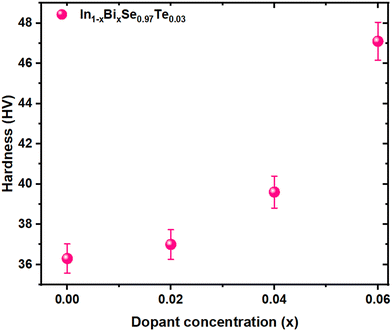 |
| | Fig. 5 Vicker's hardness value vs. dopant concentration for In1−xBixSe0.97Te0.03 (x = 0, 0.02, 0.04, 0.06) polycrystal samples. | |
3.3 Field emission scanning electron microscopy (FESEM)
FESEM serves as a high-resolution imaging approach used to investigate the surface morphology as well as the microstructure of InSe and codoped InSe polycrystals and the results are shown in Fig. 6. The samples illustrated in the images exhibit well-crystalline grains with a uniform distribution of grains. Additionally, when the dopant concentration was raised, no agglomerations or overgrowth of scattered grains were seen. The samples show a uniform and dense polycrystalline microstructure with multiscale grains that are randomly oriented. The study found that the density of the material rose slightly from 5.83 to 6.05 g cm−3 after adding the dopants. This increase is due to the inclusion of Bi and Te, which are heavier elements than In and Se, thus raising the average atomic mass of the material. As shown in Table 1, the increase in atomic mass leads to a corresponding increase in density, and these results well align with previously published data.29 The multiscale grains help to significantly lower the lattice's thermal conductivity by scattering phonons of various wavelengths. Perhaps because of the layered structure of indium selenide, the samples contain packed layered crystals.2 The layered structure is shown using arrows in the FESEM images. The surface becomes more compact as well as uniform all over the entire surface when the dopant concentration is increased from 0.02 to 0.04 to 0.06. The pure InSe and doped InSe samples exhibit a surface morphology with some localized pinholes, cracks, and voids. These features arise due to the preferential evaporation of Se atoms during synthesis.40
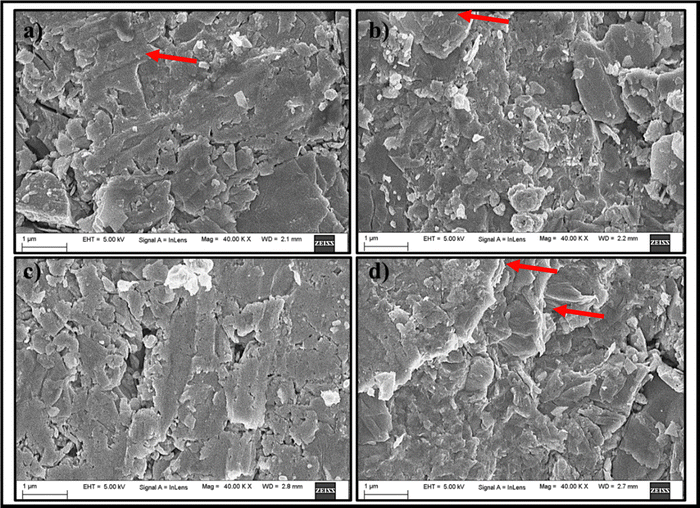 |
| | Fig. 6 FESEM images of (a) InSe, (b) In0.98Bi0.02Se0.97Te0.03, (c) In0.96Bi0.04Se0.97Te0.03 and (d) In0.94Bi0.06Se0.97Te0.03 samples. | |
3.4 Energy dispersive X-ray analysis (EDAX)
Energy-dispersive X-ray analysis (EDAX) was performed to identify the chemical composition of pristine and codoped InSe polycrystals, and the results are depicted in Fig. 7. Table 2 lists the expected and observed atomic percentages of the elements found in the samples. According to EDAX spectra, the expected and observed atomic percentages are close to each other. The elemental distribution map ensures the compositions and existence of indium and selenium in the pure indium selenide, which roughly corresponds to a 1![[thin space (1/6-em)]](https://www.rsc.org/images/entities/char_2009.gif) :
:![[thin space (1/6-em)]](https://www.rsc.org/images/entities/char_2009.gif) 1 ratio [Fig. 7a]. Dopants like Bi/Te are found to be present in doped InSe [Fig. 7(b)–(d)] and are evenly distributed throughout the synthesized samples. According to the analysis, there is an excess of In and a slight deficiency of Se. The identification of relative molars for In, Bi, Se, and Te are generally near to nominal values, indicating that the final sample compositions are nearly as intended.41
1 ratio [Fig. 7a]. Dopants like Bi/Te are found to be present in doped InSe [Fig. 7(b)–(d)] and are evenly distributed throughout the synthesized samples. According to the analysis, there is an excess of In and a slight deficiency of Se. The identification of relative molars for In, Bi, Se, and Te are generally near to nominal values, indicating that the final sample compositions are nearly as intended.41
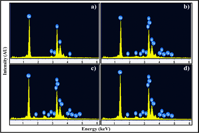 |
| | Fig. 7 EDAX images of (a) InSe, (b) In0.98Bi0.02Se0.97Te0.03, (c) In0.96Bi0.04Se0.97Te0.03 and (d) In0.94Bi0.06Se0.97Te0.03 samples. | |
Table 2 Elemental composition of In1−xBixSe0.97Te0.03 polycrystal samples
| Sample |
Elements |
Expected atomic percentage |
Observed atomic percentage |
| InSe |
In |
50 |
51.82 |
| Se |
50 |
48.18 |
| In0.98Bi0.02Se0.97Te0.03 |
In |
49 |
50.00 |
| Bi |
1.0 |
0.88 |
| Se |
48.5 |
47.89 |
| Te |
1.5 |
1.23 |
| In0.96Bi0.04Se0.97Te0.03 |
In |
48 |
49.00 |
| Bi |
2.0 |
2.0 |
| Se |
48.5 |
47.60 |
| Te |
1.5 |
1.40 |
| In0.94Bi0.06Se0.97Te0.03 |
In |
47 |
48.00 |
| Bi |
3.0 |
2.57 |
| Se |
48.5 |
48.09 |
| Te |
1.5 |
1.34 |
3.5 Electrical and thermal properties
3.5.1 Hall measurement.
The Hall carrier concentration, carrier type, and mobility of In1−xBixSe0.97Te0.03 (x = 0, 0.02, 0.04, 0.06) polycrystalline samples are investigated to determine the carrier transport in more detail. The Hall carrier concentration and mobility of the samples at 300 K are displayed in Fig. 8. The samples exhibit negative Hall coefficients, indicating that both pure and doped samples exhibit n-type semiconducting behavior, suggesting that electron carriers dominate n-type electrical conduction.41 The estimates of the electron concentration (n) in the pristine, 2%, 4%, and 6% Bi-doped samples are given in Table 3. Bi atoms occupy the In lattice in the InSe material, acting as n-type dopants that introduce extra electrons into the conduction band. This increases electron concentration, enhancing electrical conductivity. However, this doping also alters the lattice dynamics and affects the carrier mobility, which impacts the material's thermoelectric performance. It is found that the carrier concentration (n) rises from 2.36 × 1017 cm−3 to 6.77 × 1017 cm−3 as the Bi content increases from x = 0 to x = 0.06 which is about 2.86 times higher than the pristine one. On the other hand, carrier mobility decreases monotonically as the Bi content increases, from 75 cm2 V−1 s−1 for x = 0 to 44 cm2 V−1 s−1 for x = 0.06, around 1.7 times. It has been observed that there are contrasting trends between carrier concentration and mobility.30 The decreased carrier mobility with increasing Bi concentration is due to enhanced scattering from dopant atoms or defects. This increased scattering could also introduce additional phonon scattering centers, potentially reducing thermal conductivity. Bi substitution can be attributed to an increase in both carrier concentration and the impurity scattering on electrons.23 The range of carrier concentration in this data is exactly in line with previously published data.28,31 This suggests that the Bi in the InSe matrix has been successfully substituted.
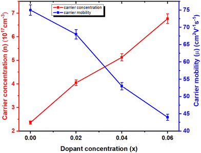 |
| | Fig. 8 The plots of mobility (μ) and carrier concentration (n) as a function of Bi doping content at 300 K for In1−xBixSe0.97Te0.03 (x = 0, 0.02, 0.04, 0.06) polycrystal samples. | |
Table 3 Carrier concentration and mobility of In1−xBixSe0.97Te0.03 samples
| Samples |
Carrier concentration, n (cm−3) × 1017 |
Mobility, μ (cm2 V−1 s−1) |
Carrier type |
| InSe |
2.36 |
75 |
n
|
| In0.98Bi0.02Se0.97Te0.03 |
3.05 |
68 |
n
|
| In0.96Bi0.04Se0.97Te0.03 |
5.13 |
53 |
n
|
| In0.94Bi0.06Se0.97Te0.03 |
6.77 |
44 |
n
|
3.5.2 Electrical conductivity (σ).
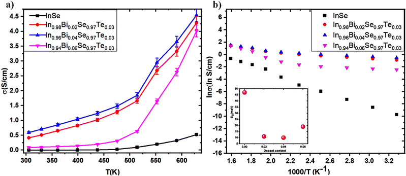
A temperature-dependent plot of electrical conductivity for In1−xBixSe0.97Te0.03 (x = 0, 0.02, 0.04, 0.06) polycrystal samples is presented in Fig. 9a. As the temperature rises, the σ value of all the samples increases which shows a semiconducting conduction behavior of the samples throughout the temperature range. The undoped InSe sample had a σ of 6.01 × 10⁻⁵ S cm−1 at 300 K. For x = 0.02, 0.04, and 0.06 Bi-doped samples, σ increased to 0.41, 0.59, and 0.08 S cm−1, respectively. σ of the undoped InSe sample was 0.52 S cm−1 at 630 K. It increased to 4.29, 4.54, and 4.01 S cm−1, respectively for x = 0.02, 0.04, and 0.06, indicating that Bi doping generally causes an increase in σ. An increase in carrier concentration is mainly responsible for the electrical conductivity that rises with increasing Bi concentration in the In1−xBixSe0.97Te0.03 matrix. Hall measurement data confirms that the substitution of Bi3+ on the cationic lattice site of In2+, which acts as a donor-type dopant in the In1−xBixSe0.97Te0.03 matrix, may be the cause of an increase in carrier concentration. At higher doping levels, such as x = 0.06, the σ value typically decreased due to decreased mobility, but σ increased for x = 0.02 and 0.04 Bi content. Across the whole temperature range, the Bi/Te-doped sample has a higher σ, and above 450 K, the increase becomes as large as about 8.73 times compared to the pristine one. The logarithmic σ values are plotted against 1000 T−1 in Fig. 9b, while the estimated activation energies (Ea) are displayed in the inset in Fig. 9b. The Arrhenius relationship,  (where k – Boltzmann constant, σ0 – pre-exponential factor, and T – absolute temperature) describes the activation energy for σ as a function of temperature.2Table 4 illustrates that the Ea is 47 meV at x = 0 Bi content. Subsequently, the Ea decreases as Bi doping increases, up to x = 0.04 concentration in In1−xBixSe0.97Te0.03 achieving 10 meV. It was found that when the amount of Bi doping reaches x = 0.06, Ea tends to increase once again. Table 4 displays the computed σ0 value, which exhibits the same pattern as Ea. These findings demonstrate that doping with small quantities of Bi positively impacts electronic transport characteristics.
 |
| | Fig. 9 (a) Electrical conductivity as a function of temperature; (b) ln![[thin space (1/6-em)]](https://www.rsc.org/images/entities/char_2009.gif) σ as a function of 1000 T−1 reveals that the slope relates to the activation energy. The estimated activation energy, Ea, is displayed in the inset for In1−xBixSe0.97Te0.03 (x = 0, 0.02, 0.04, 0.06) polycrystal samples. σ as a function of 1000 T−1 reveals that the slope relates to the activation energy. The estimated activation energy, Ea, is displayed in the inset for In1−xBixSe0.97Te0.03 (x = 0, 0.02, 0.04, 0.06) polycrystal samples. | |
Table 4 Activation energy (Ea), pre-exponential factor (σ0), effective mass, and weighted mobility (μw) of In1−xBixSe0.97Te0.03 samples
| Samples |
E
a (meV) |
σ
0 (S m−1) |
Effective mass m*/m0 |
Weighted mobility (μw) (cm2 V−1 s−1) |
| InSe |
47 |
2215 |
0.075 |
1.54 |
| In0.98Bi0.02Se0.97Te0.03 |
11 |
901 |
0.087 |
1.74 |
| In0.96Bi0.04Se0.97Te0.03 |
10 |
841 |
0.120 |
2.2 |
| In0.94Bi0.06Se0.97Te0.03 |
19 |
1166 |
0.144 |
2.4 |
3.5.3 Seebeck coefficient (S) and power factor (PF).
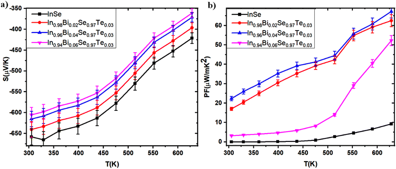
Fig. 10a depicts the temperature-dependent S value of In1−xBixSe0.97Te0.03 (x = 0, 0.02, 0.04, 0.06) polycrystal samples. The negative S values suggest that all the samples behave like n-type semiconducting materials with electrons as a majority charge carrier and agree with the hall measurement data.42 As the temperature increases, the Seebeck coefficient of every sample has been found to decrease.23 As the Bi concentration increases from x = 0 to x = 0.06, the Seebeck coefficient slightly decreased from 658 μV K−1 to 605 μV K−1 at 300 K, approximately 1.08 times lower than the pristine sample. Usually, the trend of the Seebeck coefficient opposes the electrical conductivity.43 Bi's donor doping raises the electron concentration, which results in a decrease in the Seebeck coefficient, according to Mott's relation,44| |  | (4) |
where kB – Boltzmann constant, e – electron charge, h – Planck's constant, m* – effective mass of the charge carrier, and n – carrier concentration sequentially. This relationship highlights the inverse correlation between the Seebeck coefficient (S) and carrier concentration (n), such that as n increases, S tends to decrease. In the case of Bi doping, the introduction of Bi generally leads to an elevated carrier concentration, resulting in a decrease in S. Eqn (4) was employed to calculate the effective mass using the measured values of carrier concentration and the Seebeck coefficient. Consequently, Table 4 presents the computed values of m* for both pure and doped InSe samples. The m* value was found to increase with an increase in dopant concentration. These results demonstrate donor-like behavior, confirming the substitution of Bi atoms for In atoms, and the transfer of electrons from the impurity atoms to the conduction band in InSe. Additionally, the slight decrease in the Seebeck coefficient is primarily attributed to the increase in effective mass.
 |
| | Fig. 10 (a) Seebeck coefficient and (b) power factor as a function of temperature for In1−xBixSe0.97Te0.03 (x = 0, 0.02, 0.04, 0.06) polycrystal samples. | |
The power factor (PF) of In1−xBixSe0.97Te0.03 (x = 0, 0.02, 0.04, 0.06) polycrystal samples exhibits a systematic increase with temperature, prominently illustrated in Fig. 10b. PF is determined as the product of electrical conductivity (σ) and the square of the Seebeck coefficient (S2).42 The measured parameters, including electrical conductivity (σ), Seebeck coefficient (S), carrier concentration (n), mobility (μ), and activation energy (Ea), indicate notable variation in PF between co-doped and undoped InSe samples. Specifically, at 300 K, the power factors of the In0.98Bi0.02Se0.97Te0.03, In0.96Bi0.04Se0.97Te0.03, and In0.94Bi0.06Se0.97Te0.03 samples are 17.03, 22.34, and 3.172 μW m−1 K−2, respectively, contrasting with the undoped sample (0.0026 μW m−1 K−2). As temperature increases to 630 K (Fig. 10b), the PF values escalate to 62.5, 67.27, and 52.26 μW m−1 K−2 for the In0.98Bi0.02Se0.97Te0.03, In0.96Bi0.04Se0.97Te0.03, and In0.94Bi0.06Se0.97Te0.03 samples, respectively, demonstrating a sevenfold enhancement compared to the undoped sample (9.26 μW m−1 K−2). Thus, doping induces a substantial enhancement in the power factor of the InSe sample. Remarkably, incorporating Bi atoms leads to a substantial enhancement in the PF value across the temperature range for InSe. The In0.96Bi0.04Se0.97Te0.03 sample exhibits the highest PF among all the samples investigated throughout the temperature range. This underscores the significant impact of Bi doping on improving the thermoelectric performance of InSe-based materials.
3.5.4 Thermal conductivity (κ).
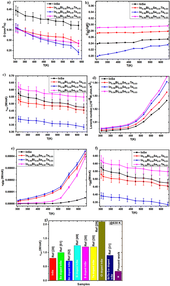
The total thermal conductivity (κtot) of a material can be conveniently estimated using the equation κtot = DCpd, where D-thermal diffusivity, Cp-specific heat capacity, and d-density.45 This approach provides an insightful framework for evaluating the thermal conductivity of synthesized samples. The thermal conductivity of a material is the sum of contributions from lattice vibrations (phonons) and charge carriers (electrons), encapsulated in the equation κtot = κlat + κele. The electronic thermal conductivity (κele) can be determined from the electrical conductivity (σ) using the Wiedemann–Franz law: κele = LσT,46 where L – Lorentz number, calculated via L = 1.5 + exp(−|S|/116),47 and T – absolute temperature. Subtracting the electronic thermal conductivity from the total thermal conductivity yields the lattice thermal conductivity (κlat), and thermal diffusivity, and specific heat capacity data are presented in Fig. 11a and b. Utilizing these graphs, the total thermal conductivity (κtot) is calculated, and is shown in Fig. 11c and the Lorentz number is depicted in Fig. 11d. Compared to pristine InSe, the κtot of all co-doped samples was found to be significantly lower. Notably, κtot decreases with an increase in dopant concentration and temperature. For example, the κtot of pristine InSe (0.475 W m−1 K−1) typically reduces to a value of approximately 0.33 W m−1 K−1 in the In0.96Bi0.04Se0.97Te0.03 sample at 630 K, which is 1.4 times lower than that of pristine InSe. The contributions of kele and klat to ktot are illustrated in Fig. 11e and f. The increase in κele is due to the increased carrier concentration in the samples, enhancing the electronic thermal transport. The In1−xBixSe0.97Te0.03 samples demonstrate lower lattice thermal conductivity values compared to pure InSe up to a Bi concentration of x = 0.04. However, at a Bi concentration of x = 0.06, the total thermal conductivity begins to increase again. This trend suggests that lower Bi content enhances the thermoelectric (TE) properties of InSe.
 |
| | Fig. 11 (a) Thermal diffusivity, (b) specific heat capacity, (c) κtot, (d) Lorentz number, (e) κele, (f) κlat plots of In1−xBixSe0.97Te0.03 (x = 0, 0.02, 0.04, 0.06) polycrystalline samples as a function of temperature and (g) comparison of κtot of this work with other published κtot values of InSe systems. | |
Moreover, the substitution of Bi and Te in the InSe matrix introduces point defects at the atomic level, which scatter phonons and contribute additional heat resistance. This phonon scattering by point defects leads to a significant reduction in lattice thermal conductivity. It is noteworthy that the contribution of κlat is more pronounced compared to κele in these samples. Due to the incredibly low recorded electrical conductivity (<5 S cm−1), electronic thermal conductivity (κele) plays a very small role in this situation. It is well known that substitutional doping adds interesting phonon scattering mechanisms. With atomic masses of 114.8 u for In and 208.9 u for Bi, and atomic radii of 80 pm for In2+ and 130 pm for Bi3+, the substitution of Bi for In results in a minor size mismatch as well as a huge mass difference. Because of these disparities in mass and size, it is anticipated that the substitution of Bi for In will increase phonon scattering.30 The large difference in atomic mass between Bi and In significantly disturbs the lattice vibrations, even with the small size difference.29,48 This perturbation increases phonon scattering, which in turn causes a significant decrease in klat. Fig. 11g provides a comprehensive comparison of κtot in various InSe systems, underscoring the enhanced thermal performance of co-doped samples.
3.5.5 Figure of merit (ZT) and quality factor (B).
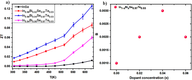
As a function of temperature, the expected ZT values are computed and displayed in Fig. 12a by combining the measured electrical and thermal properties of the In1−xBixSe0.97Te0.03 (x = 0, 0.02, 0.04, 0.06) polycrystalline samples. Through cation–anion interaction and ordered structures, the In1−xBixSe0.97Te0.03 samples systematically reduce thermal conductivity (κ) throughout the temperature range and strategically improve electrical transport properties. The carrier concentration in In1−xBixSe0.97Te0.03 is greatly optimized by Bi/Te co-doping, which raises the doped samples' electrical conductivity. Here, Bi is acting as a donor-type dopant to increase ‘n’. Additionally, the slight decrease in the Seebeck coefficient (S) is primarily due to the increase in effective mass, which leads to an enhanced power factor in doped samples.48 Additionally, this process significantly reduces lattice thermal conductivity through mass and size-dependent point-defect scattering. As a result, at 630 K, the maximum ZT increases from 0.012 for pure InSe to 0.13 for In0.96Bi0.04Se0.97Te0.03, which is ∼11 times higher than that of the pristine one. Several influential studies on InSe systems provide a comparative viewpoint, as shown in Table 5. Although the maximum ZT values reported in other works at higher temperatures (873 K or 923 K) are comparable or even superior, the ZT value of In0.96Bi0.04Se0.97Te0.03 is significantly higher across the entire temperature range of 300–630 K.
 |
| | Fig. 12 (a) Figure of merit (ZT) as a function of temperature amd (b) quality factor as a function of dopant concentration for In1−xBixSe0.97Te0.03 (x = 0, 0.02, 0.04, 0.06) polycrystal samples. | |
Table 5 Comparison of thermoelectric properties of InSe systems prepared using various techniques
| Sample |
Method |
σ (S cm−1) @630 K |
S (μV K−1) @630 K |
κ (W m−1 K−1) @630 K |
ZT @630 K |
Ref. |
|
Present work.
|
| InSe |
Melting + spark plasma sintering |
∼1.6 |
∼260 |
∼0.8 |
∼0.01 |
28
|
| InSe |
Melting + ball milling + spark plasma sintering |
∼0.25 |
∼610 |
∼1.25 |
∼0.01 |
41
|
| InSea |
Solid-state reaction |
∼0.52 |
∼425 |
∼0.475 |
∼0.012 |
— |
| Sn-doped InSe |
Solid-state reaction + spark plasma sintering |
∼3 |
∼500 |
∼1.0 |
∼0.06 |
49
|
| Sn-doped InSe |
Melting + quenching + spark plasma sintering |
∼102 |
∼250 |
∼0.7 |
∼0.26 |
50
|
| Si-doped InSe |
Solid-state reaction + Spark plasma sintering |
∼10 |
∼390 |
∼1.25 |
∼0.08 |
48
|
| S doped InSe |
Melting + spark plasma sintering |
∼4 |
∼425 |
∼1.2 |
∼0.1 |
30
|
| Te doped InSe |
Melting + spark plasma sintering |
∼11 |
∼390 |
∼1.2 |
∼0.23 |
30
|
| Cl-doped InSe |
Melting + spark plasma sintering |
∼3.6 |
∼560 |
∼2.1 |
∼0.039 |
29
|
| Si/Te co-doped InSe |
Solid-state reaction + spark plasma sintering |
∼5.5 |
∼425 |
∼0.9 |
∼0.085 |
31
|
| In0.96Bi0.04Se0.97Te0.03a |
Solid-state reaction method |
∼4.54 |
∼380 |
∼0.33 |
∼0.13 |
— |
The weighted mobility (μw) is given by ref. 51,
| |  | (5) |
where
μ – carrier mobility,
m* – effective mass,
m0 – rest mass of electron.
Table 4 presents the values of
μw and the effective mass (
m*/
m0) at 300 K for In
1−xBi
xSe
0.97Te
0.03 samples. The trend observed in
μw mirrors the trend in
m*/
m0, as
μw is proportional to
m*/
m0 according to
eqn (4). All doped samples exhibited an improvement in
μw compared to the undoped sample.
Fig. 12b illustrates the quality factor (
B) for polycrystalline samples of In
1−xBi
xSe
0.97Te
0.03 (
x = 0, 0.02, 0.04, 0.06) at 300 K. The dimensionless thermoelectric quality factor (
B) was calculated using the equation,
51| |  | (6) |
‘
B’ calculations are based on the intrinsic thermoelectric properties of the samples. Notably, In
0.96Bi
0.04Se
0.97Te
0.03 exhibited the lowest lattice thermal conductivity, resulting in a maximum
B value of approximately 0.003 at 300 K. This study demonstrates that co-doping is an effective strategy for introducing appropriate dopants to optimize the collective thermoelectric transport properties. The findings suggest that the enhanced
ZT values in InSe-based materials hold significant promise for future thermoelectric applications, underscoring the potential of co-doping to achieve superior performance in thermoelectric devices.
Using a simple solid-state reaction method, we observed significantly lower thermal conductivity compared to other studies. This method typically produces materials with well-defined crystal structures, enhancing phonon scattering, reducing thermal conductivity, and ensuring uniform dopant distribution. Solid-state synthesis, performed in controlled environments with fewer processing steps, results in higher chemical purity. Additionally, it allows for precise control over the material's microstructure, morphology, and porosity, which critically impacts the transport properties. These benefits highlight the effectiveness of the solid-state metathesis route in enhancing material performance for various applications.
Bi and Te co-doped InSe samples demonstrate superior thermoelectric performance at 630 K, achieving a ZT of ∼0.13, which exceeds values reported in previous studies. Although other studies, such as those by Ji-il Kim et al.30 indicate that InSe achieves higher ZT values at elevated temperatures, the current measurements were constrained to 630 K due to instrumental limitations. Given the observed trends of reduced thermal conductivity and enhanced electrical conductivity, it is plausible that the sample could achieve even higher ZT values at temperatures beyond 630 K. Therefore, future work should focus on studying the thermoelectric properties of this material at elevated temperatures above 630 K to fully assess its potential for thermoelectric applications.
4. Conclusion
In summary, polycrystalline samples of In1−xBixSe0.97Te0.03 (x = 0.0, 0.02, 0.04, 0.06) were synthesized using a solid-state reaction technique. The co-doping of Bi and Te in InSe led to significant enhancements in thermoelectric properties: Bi increases carrier concentration and electrical conductivity while causing a slight reduction in the Seebeck coefficient. Additionally, Bi and Te co-doping introduce point defects that reduce total thermal conductivity (κtot). The optimized samples achieved a power factor of approximately 67.27 μW m−1 K−2, which is seven times higher than that of pristine InSe, and a reduced κtot of about 0.33 W m−1 K−1. Specifically, the In0.96Bi0.04Se0.97Te0.03 sample reached a maximum ZT of ∼0.13 at 630 K, eleven times higher than the pristine InSe. These findings indicate that Bi and Te codoped InSe is a promising candidate for applications in power generation. Future research should focus on refining doping concentrations, investigating other co-dopants, and further reducing thermal conductivity to optimize the thermoelectric performance of InSe-based materials.
Author contributions
Manasa R Shankar: methodology, investigation, analysis, writing – original draft. A. N. Prabhu: supervision, validation, writing – review & editing. Tulika Srivastava: resources, data curation.
Data availability
The corresponding author can provide the data used in this study upon request.
Conflicts of interest
The authors certify that they have no known conflicts of interest about money or personal connections that might have influenced the work that was done for this paper.
Acknowledgements
The author wishes to thank the Manipal Academy of Higher Education for providing financial assistance through the Dr T. M. A. doctoral fellowship. The author would like to acknowledge Vighnesh K. R., Glass Processing Lab, MIT, MAHE, for his assistance with density measurement, as well as the Head, Mechanical Engineering Department, MIT, MAHE, for providing the Hardness measurement facility and Dr Vikas Mishra for his support. ANP would like to acknowledge MAHE for providing intramural funds (MAHE/CDS/PHD/IMF/2022).
References
- Y. Pan,
et al., Recent advances in synthesis, modification and photocatalytic applications of micro/nano-structured zinc indium sulfide, Chem. Eng. J., 2018, 354, 407–431, DOI:10.1016/j.cej.2018.08.028.
- P. Dhama, A. Kumar and P. Banerji, Combined effects of indium nanoinclusion and Se-deficiency on thermoelectric performance of n-type indium selenide, J. Alloys Compd., 2022, 901, 163653, DOI:10.1016/j.jallcom.2022.163653.
- P. Sharma, A. Dahshan, V. K. Sehgal and K. A. N. Aly, High Thermoelectric Action in Vacuum Deposited Indium Alloyed Chalcogenide Thin Films: InxSe100−x, IEEE Trans. Electron Devices, 2018, 65(8), 3408–3413, DOI:10.1109/TED.2018.2845413.
- L. W. Sprague, C. Huang, J. P. Song and B. M. Rubenstein, Maximizing Thermoelectric Figures of Merit by Uniaxially Straining Indium Selenide, J. Phys. Chem. C, 2019, 123(41), 25437–25447, DOI:10.1021/acs.jpcc.9b05681.
- P. P. Murmu,
et al., Role of phase separation in nanocomposite indium-tin-oxide films for transparent thermoelectric applications, J. Materiomics, 2021, 7(3), 612–620, DOI:10.1016/j.jmat.2020.10.015.
- R. Haleoot and B. Hamad, Thermoelectric properties of doped β-InSe by Bi: First principle calculations, Phys. B, 2020, 587, 412105, DOI:10.1016/j.physb.2020.412105.
- B. Zhou,
et al., Thermoelectric properties of SnS with Na-doping, ACS Appl. Mater. Interfaces, 2017, 9(39), 34033–34041, DOI:10.1021/acsami.7b08770.
- X. Qian,
et al., Synergistically optimizing interdependent thermoelectric parameters of n-type PbSe through alloying CdSe, Energy Environ. Sci., 2019, 12(6), 1969–1978, 10.1039/c8ee03386b.
- D. Liu, X. Li, P. M. De Castro Borlido, S. Botti, R. Schmechel and M. Rettenmayr, Anisotropic layered Bi2Te3–In2Te3 composites: Control of interface density for tuning of thermoelectric properties, Sci. Rep., 2017, 7, 1–13, DOI:10.1038/srep43611.
- N. H. Tran Nguyen,
et al., Thermoelectric Properties of Indium and Gallium Dually Doped ZnO Thin Films, ACS Appl. Mater. Interfaces, 2016, 8(49), 33916–33923, DOI:10.1021/acsami.6b10591.
- A. A. Olvera,
et al., Partial indium solubility induces chemical stability and colossal thermoelectric figure of merit in Cu2Se, Energy Environ. Sci., 2017, 10(7), 1668–1676, 10.1039/c7ee01193h.
- Y. Xiao and L. D. Zhao, Charge and phonon transport in PbTe-based thermoelectric materials, npj Quantum Mater., 2018, 3, 55, DOI:10.1038/s41535-018-0127-y.
- J. Sun, Y. Zhang, Y. Fan, X. Tang and G. Tan, Strategies for boosting thermoelectric performance of PbSe: a review, Chem. Eng. J., 2022, 431(P4), 133699, DOI:10.1016/j.cej.2021.133699.
- L. Zhang, J. Wang, Z. Cheng, Q. Sun, Z. Li and S. Dou, Lead-free SnTe-based thermoelectrics: Enhancement of thermoelectric performance by doping with Gd/Ag, J. Mater. Chem. A, 2016, 4(20), 7936–7942, 10.1039/c6ta01994c.
- Y. L. Lee,
et al., Data-Driven Enhancement of ZT in SnSe-Based Thermoelectric Systems, J. Am. Chem. Soc., 2022, 144(30), 13748–13763, DOI:10.1021/jacs.2c04741.
- H. Zhu, G. Wang, G. Wang, X. Zhou and X. Lu, The role of electronic affinity for dopants in thermoelectric transport properties of InTe, J. Alloys Compd., 2021, 869, 1–6, DOI:10.1016/j.jallcom.2021.159224.
- P. Mannu, M. Palanisamy, G. Bangaru, S. Ramakrishnan, M. Ramcharan and A. Kandasami, Electrical transport properties of Indium chalcogenide thin films and their thermoelectric applications, Mater. Today: Proc., 2019, 48(xxxx), 115–118, DOI:10.1016/j.matpr.2020.02.675.
- I. Alexandrescu, C. Teodosiu and A. Maftei, Environmental and ecotoxicological risk of lead compounds, Environ. Eng Manage. J., 2003, 2(3), 255–270, DOI:10.30638/eemj.2003.024.
- K. Imai, K. Suzuki, T. Haga, Y. Hasegawa and Y. Abe, Phase diagram of In-Se system and crystal growth of indium monoselenide, J. Cryst. Growth, 1981, 54(3), 501–506, DOI:10.1016/0022-0248(81)90505-4.
- P. B. Patel, J. M. Dhimmar, B. P. Modi and H. N. Desai, The advancement of compelling Indium Selenide: synthesis, structural studies, optical properties and photoelectrical applications, J. Mater. Sci.: Mater. Electron., 2021, 32(1), 1033–1041, DOI:10.1007/s10854-020-04878-3.
- D. W. Boukhvalov,
et al., The advent of indium selenide: Synthesis, electronic properties, ambient stability and applications, Nanomaterials, 2017, 7(11), 1–16, DOI:10.3390/nano7110372.
- G. Han, Z. G. Chen, J. Drennan and J. Zou, Indium selenides: structural characteristics, synthesis and their thermoelectric performances, Small, 2014, 10(14), 2747–2765, DOI:10.1002/smll.201400104.
- R. Haleoot and B. Hamad, Thermoelectric properties of doped β-InSe by Bi: first principle calculations, Phys. B, 2020, 587, 412105, DOI:10.1016/j.physb.2020.412105.
- M. Küpers,
et al., Controlled Crystal Growth of Indium Selenide, In2Se3, and the Crystal Structures of α-In2Se3, Inorg. Chem., 2018, 57(18), 11775–11781, DOI:10.1021/acs.inorgchem.8b01950.
- Y. Zhai,
et al., Thermoelectric performance of the ordered In4Se3-in composite constructed by monotectic solidification, J. Mater. Chem. A, 2013, 1(31), 8844–8847, 10.1039/c3ta01599h.
- S. Mori, Electrical Properties of In6Se7, J. Phys. Soc. Jpn., 1973, 35(1), 310, DOI:10.1143/JPSJ.35.310.
- P. Matheswaran, R. Saravana Kumar and R. Sathyamoorthy, Effect of annealing on the structural and optical properties of InSe bilayer thin films, Vacuum, 2011, 85(8), 820–826, DOI:10.1016/j.vacuum.2010.12.004.
- J. Yoo,
et al., Electronic and Thermal Properties of Si-doped InSe Layered Chalcogenides, J. Korean Phys. Soc., 2018, 72(7), 775–779, DOI:10.3938/jkps.72.775.
- S. W. Lee, T. Kim, H. S. Kim, O. Park, D. H. Kim and S. Il Kim, Enhanced thermoelectric properties of InSe through simultaneous increase in electrical conductivity and Seebeck coefficient by Cl doping, J. Mater. Res. Technol., 2022, 19, 2077–2083, DOI:10.1016/j.jmrt.2022.05.180.
- J. Il Kim, H. S. Kim and S. Il Kim, Electrical and thermal transport properties of S- and Te-doped InSe alloys, J. Phys. D: Appl. Phys., 2019, 52, 295501, DOI:10.1088/1361-6463/ab1caa.
- J. H. Jeon,
et al., Thermoelectric Properties of Te-doped In0.9Si0.1Se with Enhanced Effective Mass, Electron. Mater. Lett., 2021, 17(4), 340–346, DOI:10.1007/s13391-021-00278-9.
- A. A. A. Darwish, M. M. El-Nahass and M. H. Bahlol, Structural and electrical studies on nanostructured InSe thin films, Appl. Surf. Sci., 2013, 276, 210–216, DOI:10.1016/j.apsusc.2013.03.068.
- U. Deepika Shanubhogue, A. Pal, A. Rao, S. Chattopadhyay, A. M. Ashok and N. Davis, Tuning optical and thermoelectric properties of LaCoO3: partial substitution of La by isovalent Gd, J. Alloys Compd., 2023, 941, 168987, DOI:10.1016/j.jallcom.2023.168987.
- T. Mathew, A. G. Kunjomana, K. Munirathnam, K. A. Chandrasekharan, M. Meena and C. K. Mahadevan, Mechanical and Dielectric Properties of InTe Crystals, Cryst. Struct. Theory Appl., 2012, 01(03), 79–83, DOI:10.4236/csta.2012.13015.
- M. R. Shankar, A. N. Prabhu, A. M. Ashok, N. Davis, B. Srinivasan and V. Mishra, Role of Bi/Te co-dopants on the thermoelectric properties of SnSe polycrystals: an experimental and theoretical investigation, J. Mater. Sci., 2024, 59(28), 13055–13077, DOI:10.1007/s10853-024-09984-9.
- B. Nan,
et al., Bottom-Up Synthesis of SnTe-Based Thermoelectric Composites, ACS Appl. Mater. Interfaces, 2023, 15(19), 23380–23389, DOI:10.1021/acsami.3c00625.
- H. Watson,
et al., Author’ s Accepted Manuscript Author’ s Accepted Manuscript, Prostaglandins, Leukotrienes Essent. Fatty Acids, 2016, 115, 60–66, DOI:10.1097/JU.0000000000002945.
- S. J. Brito-Garcia, J. C. Mirza-Rosca, C. Jimenez-Marcos and I. Voiculescu, Impact of Ti Doping on the Microstructure and Mechanical Properties of CoCrFeMoNi High-Entropy Alloy, Metals, 2023, 13(5), 1–13, DOI:10.3390/met13050854.
- L. Zhao,
et al., The Effects of Te2− and I− Substitutions on the Electronic Structures, Thermoelectric Performance, and Hardness in Melt-Quenched Highly Dense Cu2−xSe, Adv. Electron. Mater., 2015, 1(3), 1–8, DOI:10.1002/aelm.201400015.
- Y. Yan,
et al., Influence of indium concentration on the structural and optoelectronic properties of indium selenide thin films, Opt. Mater., 2014, 38, 217–222, DOI:10.1016/j.optmat.2014.10.033.
- X. Hou, S. Chen, Z. Du, X. Liu and J. Cui, Improvement of the thermoelectric performance of InSe-based alloys doped with Sn, RSC Adv., 2015, 5(124), 102856–102862, 10.1039/c5ra23023c.
- J. S. Rhyee and J. H. Kim, Chemical potential tuning and enhancement of thermoelectric properties in Indium Selenides, Materials, 2015, 8(3), 1283–1324, DOI:10.3390/ma8031283.
- X. Tan,
et al., Optimizing the thermoelectric performance of In–Cd codoped SnTe by introducing Sn vacancies, J. Mater. Chem. C, 2017, 5(30), 7504–7509, 10.1039/c7tc02162c.
- X. Yin, J. Y. Liu, L. Chen and L. M. Wu, High Thermoelectric Performance of In4Se3-Based Materials and the Influencing Factors, Acc. Chem. Res., 2018, 51(2), 240–247, DOI:10.1021/acs.accounts.7b00480.
- H. Tan,
et al., Synergistic Effect of Bismuth and Indium Codoping for High Thermoelectric Performance of Melt Spinning SnTe Alloys, ACS Appl. Mater. Interfaces, 2019, 11(26), 23337–23345, DOI:10.1021/acsami.9b05880.
- S. Perumal, P. Bellare, U. S. Shenoy, U. V. Waghmare and K. Biswas, Low Thermal Conductivity and High Thermoelectric Performance in Sb and Bi Codoped GeTe: Complementary Effect of Band Convergence and Nanostructuring, Chem. Mater., 2017, 29(24), 10426–10435, DOI:10.1021/acs.chemmater.7b04023.
- T. Wang,
et al., Thermoelectric performance of SnTe alloys with In and Sb co-doped near critical solubility limit, J. Mater. Sci., 2019, 54(12), 9049–9062, DOI:10.1007/s10853-019-03502-y.
- K. H. Lee,
et al., Enhanced thermoelectric transport properties of n-type InSe due to the emergence of the flat band by Si doping, Inorg. Chem. Front., 2019, 6(6), 1475–1481, 10.1039/c9qi00210c.
- S. S. Choo, S. W. Hong and H. S. Kim, and S. Il Kim, Enhanced thermoelectric transport properties of n-type InSe by Sn doping, Taehan Kumsok·Chaeryo Hakhoechi, 2020, 58(5), 348–352, DOI:10.3365/KJMM.2020.58.5.348.
- Y. Zhai,
et al., Thermoelectric properties of In1.3xSnxSe prepared by spark plasma sintering method, J. Alloys Compd., 2013, 553, 270–272, DOI:10.1016/j.jallcom.2012.11.139.
- G. J. Snyder, A. H. Snyder, M. Wood, R. Gurunathan, B. H. Snyder and C. Niu, Weighted Mobility, Adv. Mater., 2020, 32(25), 1–5, DOI:10.1002/adma.202001537.
|
| This journal is © The Royal Society of Chemistry 2024 |
Click here to see how this site uses Cookies. View our privacy policy here.  Open Access Article
 *a and
Tulika
Srivastava
b


![[thin space (1/6-em)]](https://www.rsc.org/images/entities/char_2009.gif) cos
cos![[thin space (1/6-em)]](https://www.rsc.org/images/entities/char_2009.gif) θ on the y-axis vs. 4
θ on the y-axis vs. 4![[thin space (1/6-em)]](https://www.rsc.org/images/entities/char_2009.gif) sin
sin![[thin space (1/6-em)]](https://www.rsc.org/images/entities/char_2009.gif) θ on the x-axis enables the line (y = mx + c) to be fitted to the data. Fig. 4 shows the experiment data as well as the fitted graphs. The strain values were calculated using the line's slope (ε = m), and the crystallite size was determined using the line's intercept (D = kλ/c). The crystallite size is found to typically range between 47 and 76 nm using the WH technique. Impurities known as dopants can function as point defects in polycrystalline materials, increasing the strain on the lattice. Dopants can modify the lattice parameters in addition to raising strain.
θ on the x-axis enables the line (y = mx + c) to be fitted to the data. Fig. 4 shows the experiment data as well as the fitted graphs. The strain values were calculated using the line's slope (ε = m), and the crystallite size was determined using the line's intercept (D = kλ/c). The crystallite size is found to typically range between 47 and 76 nm using the WH technique. Impurities known as dopants can function as point defects in polycrystalline materials, increasing the strain on the lattice. Dopants can modify the lattice parameters in addition to raising strain.


![[thin space (1/6-em)]](https://www.rsc.org/images/entities/char_2009.gif) :
:![[thin space (1/6-em)]](https://www.rsc.org/images/entities/char_2009.gif) 1 ratio [Fig. 7a]. Dopants like Bi/Te are found to be present in doped InSe [Fig. 7(b)–(d)] and are evenly distributed throughout the synthesized samples. According to the analysis, there is an excess of In and a slight deficiency of Se. The identification of relative molars for In, Bi, Se, and Te are generally near to nominal values, indicating that the final sample compositions are nearly as intended.41
1 ratio [Fig. 7a]. Dopants like Bi/Te are found to be present in doped InSe [Fig. 7(b)–(d)] and are evenly distributed throughout the synthesized samples. According to the analysis, there is an excess of In and a slight deficiency of Se. The identification of relative molars for In, Bi, Se, and Te are generally near to nominal values, indicating that the final sample compositions are nearly as intended.41


 (where k – Boltzmann constant, σ0 – pre-exponential factor, and T – absolute temperature) describes the activation energy for σ as a function of temperature.2Table 4 illustrates that the Ea is 47 meV at x = 0 Bi content. Subsequently, the Ea decreases as Bi doping increases, up to x = 0.04 concentration in In1−xBixSe0.97Te0.03 achieving 10 meV. It was found that when the amount of Bi doping reaches x = 0.06, Ea tends to increase once again. Table 4 displays the computed σ0 value, which exhibits the same pattern as Ea. These findings demonstrate that doping with small quantities of Bi positively impacts electronic transport characteristics.

