Electron beam lithography of GeTe through polymorphic phase transformation†
Hu
Zhang‡
abc,
Meng
Li‡
d,
Shao-Bo
Mi
 *a,
Shao-Dong
Cheng
c,
Lu
Lu
a and
Zhi-Gang
Chen
 *d
*d
aJi Hua Laboratory, Foshan 528200, China. E-mail: mi_jhlab@163.com
bSchool of Physics and Information Technology, Shaanxi Normal University, Xi’an 710119, China
cState Key Laboratory for Mechanical Behavior of Materials & School of Microelectronics, Xi’an Jiaotong University, Xi’an 710049, China
dSchool of Chemistry & Physics, Faculty of Science, Queensland University of Technology, Queensland 4000, Australia. E-mail: zhigang.chen@qut.edu.au
First published on 12th July 2024
Abstract
We report two previously undiscovered phases of GeTe including the sphalerite (c-) phase and the hexagonal (h-) phase with interlayer van der Waals gaps. A polymorphic phase transformation from rhombohedral α-GeTe to c- and h-GeTe at near room temperature is first realized via electron beam irradiation. Their underlying thermodynamics and kinetics are illustrated using the in situ heating experiments and molecular dynamics simulations. Density-functional theory calculations indicate that c-GeTe exhibits typical metallic behavior and h-GeTe is a narrow-gap semiconductor with a strong spin–orbital coupling effect. Our findings shed light on a strategy for designing GeTe-based quantum devices compromising nanopillars and heterostructures via an atomic-scale electron beam lithography technique.
New conceptsFinding new phases can help deeply understand the fundamentals of materials and broaden their practical applications. Particularly, locally tailoring the crystal structure of materials at the atomic scale through phase transitions in scanning transmission electron microscopy can tune their physical and chemical properties. It is a proof-of-concept that two previously unreported phases of GeTe, the sphalerite (c-) phase and the hexagonal (h-) phase with interlayer van der Waals gaps, are first realized by electron beam irradiation on α-GeTe. Moreover, an atomic-scale electron beam lithography technique is developed and adopted to fabricate GeTe-based quantum devices compromising nanopillars and heterostructures of c- and h-GeTe in the α-GeTe matrix, offering a strategy for enhancing and extending the application range of GeTe-based materials. |
Introduction
As a historic member of group IV–VI chalcogenides, germanium telluride (GeTe) was first known for its non-volatile ovonic memory switching behavior, which can be applied for high-speed, high-density, and multi-value memory technologies.1–3 More recently, investigations on GeTe and its derivative antimonides and bismuthides have resurged, with heightened interest surrounding their intriguing phase-change crystallography,4 nature of chemical bonds,5 and underlying physical and chemical fundamentals.6 Particularly, such a family of materials exhibits desirable electronic and thermal transport characteristics for thermoelectricity,7–9 ferroelectricity,10–12 information storage,13 and superconductivity.14 These functionalities are based mainly on the entanglement or decoupling between the amorphous and crystalline phases of GeTe, thus being sensitive to the corresponding phase transformation.Pristine GeTe alone undergoes a ferroelectric-like, reversible, and quasi-second ordered phase transformation from low-temperature rhombohedral α-GeTe (R3m) to high-temperature face-centered cubic β-GeTe (Fm![[3 with combining macron]](https://www.rsc.org/images/entities/char_0033_0304.gif) m) at a Curie temperature (Tc) of ∼720 K.15 Specifically, in β-GeTe, the central Ge atom is six-fold coordinated with neighboring Te atoms, resulting in an Oh chemical bond scheme.16 During the phase transformation, the Oh coordination symmetry switches to C3v through splitting the six equivalent Ge–Te bonds into three long metavalent bonds and three short dative bonds.17 Meanwhile, the rocksalt-type lattice of β-GeTe randomly shears along the four Peierls distortion vectors, i.e., [111], [
m) at a Curie temperature (Tc) of ∼720 K.15 Specifically, in β-GeTe, the central Ge atom is six-fold coordinated with neighboring Te atoms, resulting in an Oh chemical bond scheme.16 During the phase transformation, the Oh coordination symmetry switches to C3v through splitting the six equivalent Ge–Te bonds into three long metavalent bonds and three short dative bonds.17 Meanwhile, the rocksalt-type lattice of β-GeTe randomly shears along the four Peierls distortion vectors, i.e., [111], [![[1 with combining macron]](https://www.rsc.org/images/entities/char_0031_0304.gif) 11], [1
11], [1![[1 with combining macron]](https://www.rsc.org/images/entities/char_0031_0304.gif) 1], and [
1], and [![[1 with combining macron]](https://www.rsc.org/images/entities/char_0031_0304.gif)
![[1 with combining macron]](https://www.rsc.org/images/entities/char_0031_0304.gif) 1], resulting in simultaneous polarization of Ge and Te sublattices.18 The phase-change-induced evolutionary crystal structure and bonding mechanism lead to exceptional optical absorption and dielectric constants, and an unconventionally large Born effective charge, making GeTe have competent diverse functionalities.19 Discovering additional phases is therefore crucial for broadening the application scope of GeTe-based functional materials. In fact, there have been previous reports of orthorhombic γ-GeTe (Pnma),20 orthorhombic δ-GeTe (Pbcn),21 and monoclinic ε-GeTe (Cm),22 which are achieved either with non-stoichiometry or under ultrahigh isometric pressure, being exempt from scalable synthesis and practical applications. As a result, exploring easily achievable new phases of GeTe is still an open challenge in this field.
1], resulting in simultaneous polarization of Ge and Te sublattices.18 The phase-change-induced evolutionary crystal structure and bonding mechanism lead to exceptional optical absorption and dielectric constants, and an unconventionally large Born effective charge, making GeTe have competent diverse functionalities.19 Discovering additional phases is therefore crucial for broadening the application scope of GeTe-based functional materials. In fact, there have been previous reports of orthorhombic γ-GeTe (Pnma),20 orthorhombic δ-GeTe (Pbcn),21 and monoclinic ε-GeTe (Cm),22 which are achieved either with non-stoichiometry or under ultrahigh isometric pressure, being exempt from scalable synthesis and practical applications. As a result, exploring easily achievable new phases of GeTe is still an open challenge in this field.
In this work, we report two room-temperature-stable phases of GeTe that have never been observed, namely sphalerite c-GeTe and hexagonal h-GeTe with interlayer van der Waals gaps. Specifically, we first tailor the polymorphic phase transformation from α-GeTe to c-GeTe and h-GeTe via electron beam irradiation, which supposedly ends in β-GeTe above Tc. The thermodynamic and kinetic features behind this phenomenon are theoretically explained by the stereochemical expression of Ge 4s2 lone pairs and experimentally verified based on in situ heating experiments. We further performed density functional theory (DFT) calculations to understand the electronic transport characteristics of inclusive phases at the fundamental level. Last but foremost, two proof-of-concept GeTe-based quantum devices are successfully fabricated through patterning nanopillar arrays and heterostructures of h-GeTe and c-GeTe superlattices in the α-GeTe matrix via electron beam irradiation, offering a feasible method for enhancing and extending the application range of GeTe-based compounds.
Results and discussion
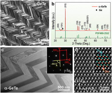
The microstructures and phase purities of the as-prepared samples have been studied by X-ray diffraction (XRD) and scanning electron microscopy (SEM, see Fig. S1, ESI†). Fig. 1a displays a typical secondary electron SEM image of the fractured cross-section, which exhibits a typical herringbone structure with periodic twinning motifs. The alternative contrast between adjacent twinned domains should be attributed to the different variants of ferroelectric polarization when cooling from β-GeTe to α-GeTe. Fig. 1b shows an XRD pattern of the as-prepared GeTe sample at room temperature, where the majority of diffraction peaks can be indexed as α-GeTe. Additionally, a minor Ge impurity phase (<5 wt%) can be trackable, indicating that the major GeTe phase is Ge-deficient according to the nominal composition designed for the ingot. The lattice parameters of α-GeTe are calculated to be a = 4.170(1) Å and c = 10.672(9) Å, being consistent with previous literature.23–25 To simplify the discussion, for the time being, we consider α-GeTe as the pseudo-cubic analogy of β-GeTe with a lattice parameter of a = 5.900 Å, and mark relevant planes and axes with subscripted “pc”. The bright-field transmission electron microscopy (BF-TEM) image of GeTe in Fig. 1c displays a contrast variation periodically owing to the twinned domain stacking in α-GeTe.26,27 The inset showing the selected-area electron diffraction (SAED) pattern obtained from a single domain of the TEM specimen further elucidates the crystallographic orientation characteristics of α-GeTe on the [1![[1 with combining macron]](https://www.rsc.org/images/entities/char_0031_0304.gif) 0]pc zone axis, showing an angle of ∼88.5° between (002)pc and (220)pc planes. Fig. 1d shows an atomic-resolution high-angle annular dark-field scanning transmission electron microscopy (HAADF-STEM) image of α-GeTe taken along the [1
0]pc zone axis, showing an angle of ∼88.5° between (002)pc and (220)pc planes. Fig. 1d shows an atomic-resolution high-angle annular dark-field scanning transmission electron microscopy (HAADF-STEM) image of α-GeTe taken along the [1![[1 with combining macron]](https://www.rsc.org/images/entities/char_0031_0304.gif) 0]pc zone axis, indicating the off-centering displacement of Ge from the high-symmetry ground state along the 〈111〉pc direction. The corresponding superposed structure model of α-GeTe from the simulated HAADF-STEM image is provided in the inset for visualization.
0]pc zone axis, indicating the off-centering displacement of Ge from the high-symmetry ground state along the 〈111〉pc direction. The corresponding superposed structure model of α-GeTe from the simulated HAADF-STEM image is provided in the inset for visualization.
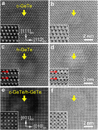
Modulating vacancies in Ge-deficient GeTe via nanosecond pulsed laser radiation to alter the multilevel reversible electrical conductivity of GeTe films has been previously reported.28,29 Other notable reports are about tuning the vacancy ordering in Ge2Sb2Te5via electron beam irradiation,30–32 which leads to the occurrence of unique optical, electrical, and thermal properties in the modified materials.33 In our experiment, we vary the time of electron beam irradiation on the region of interest (ROI) and simultaneously take corresponding atomic-resolution HAADF- and annular bright-field (ABF)-STEM images in the 〈100〉pc and 〈110〉pc zone axes of α-GeTe. In the HAADF-STEM mode, the intensity of the atomic column is roughly proportional to the squared atomic number (Z2),34 based on which the Te sublattice can be clearly distinguished from the Ge sublattice. Moreover, as a supplement, the sublattice of the light element Ge can be well recognized in the ABF-STEM mode.35 As can be seen in Fig. 2a and b, compared with the pristine α-GeTe, the ∼5 × 5 nm2 ROI in the α-GeTe matrix becomes unstable when the probe current of the electron beam is above 6.4 pA cm−2, corresponding to a beam intensity of 1.6 × 1026 e m−2 s−1. After 240 s of continuous electron beam irradiation, the Ge sublattices in the ROI are displaced along the 〈111〉pc direction, while the Te sublattices are arguably unaffected, leading to the formation of an unreported face-centered cubic phase of GeTe (see Movie S1 and Fig. S2, ESI†), here named as c-GeTe.
By extending the electron beam irradiation to 500 s, further re-arrangement of Ge sublattices can occur, while Te sublattices, as one would expect, remain almost the same (see Fig. 2c and d). This leads to another unreported layered hexagonal phase of GeTe, here named as h-GeTe (see Movie S1 and Fig. S2, ESI†). Unlike the –Te –Ge– stacking sequence along the 〈111〉pc direction in α-GeTe, the –Te–Ge–Ge–Te– stacking sequence appears in h-GeTe due to the simultaneous convergence of two adjacent Ge layers and divergence of two adjacent Te layers. As a consequence, in h-GeTe van der Waals (vdW) gaps exist between adjacent quadruple atomic layers.36 Supplementary HAADF- and ABF-STEM images of ROI in the 〈100〉pc zone axis are presented in Fig. 2e and f. As can be seen, while the Ge and Te atomic columns of α-GeTe are overlapped when viewed in such a zone axis, they can be distinguished in c-GeTe and h-GeTe phases, where the Ge atomic column lies among four neighboring Te atomic columns (see Fig. S3, ESI†). It is worth mentioning that no other crystalline phases appear by further extending the electron beam irradiation (e.g., about 5000 s).
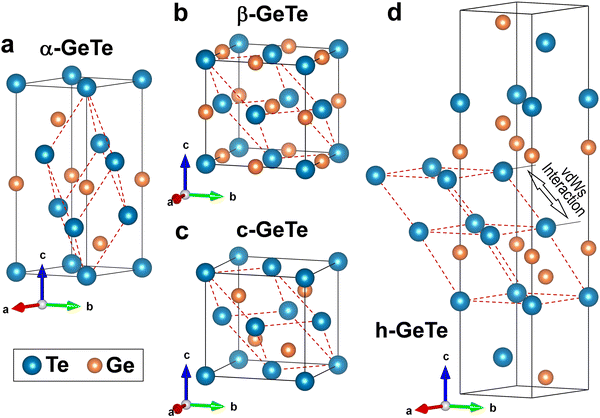
The preceding micrographs suggest that both c-GeTe and h-GeTe belong to distinct coordination symmetries and space groups compared with those of α-GeTe and β-GeTe. Fig. 3a–d display conventional cells of α-GeTe, β-GeTe, c-GeTe, and h-GeTe. In addition, the primitive cell of α-GeTe, β-GeTe, and c-GeTe, and the structure unit of h-GeTe containing vdW gap are illustrated by red broken-line frames in Fig. 3a–d. The evolution from α-GeTe to c-GeTe originates from the displacement of the central Ge atom in the GeTe6 octahedron along the 〈111〉pc direction, which is ultimately in the interstitial of the GeTe4 tetrahedron. c-GeTe is therefore identified as the sphalerite structure (F![[4 with combining macron]](https://www.rsc.org/images/entities/char_0034_0304.gif) 3m, Fig. 3c). A cube-on-cube orientation relationship (OR) can be described between α-GeTe and c-GeTe. It is necessary to mention that no apparent diffusion of Ge atoms occurs between the ROI and the surrounding α-GeTe matrix (see Fig. S4, ESI†).
3m, Fig. 3c). A cube-on-cube orientation relationship (OR) can be described between α-GeTe and c-GeTe. It is necessary to mention that no apparent diffusion of Ge atoms occurs between the ROI and the surrounding α-GeTe matrix (see Fig. S4, ESI†).
The evolution from c-GeTe to h-GeTe can be regarded as one Ge atom hopping from the interstitial of the GeTe4 tetrahedron to the center of the adjacent vacant Te tetrahedron. Meanwhile, the two as-formed consecutive Te tetrahedra form vdW gaps between two Te atomic layers. h-GeTe is therefore identified as the hexagonal structure with an inversion center (R![[3 with combining macron]](https://www.rsc.org/images/entities/char_0033_0304.gif) m, Fig. 3d), which has an OR of h-GeTe(0001)[11
m, Fig. 3d), which has an OR of h-GeTe(0001)[11![[2 with combining macron]](https://www.rsc.org/images/entities/char_0032_0304.gif) 0]//α-GeTe(111)pc[1
0]//α-GeTe(111)pc[1![[1 with combining macron]](https://www.rsc.org/images/entities/char_0031_0304.gif) 0]pc relative to the α-GeTe matrix.
0]pc relative to the α-GeTe matrix.
Note that in the course of phase transition induced by electron-beam irradiation, the c-GeTe and h-GeTe phases can co-exist in a single ROI (see Fig. S5 and Movie S1, ESI†). In addition, in contrast to the chemical stoichiometry of α-GeTe measured by energy dispersive X-ray spectroscopy (EDS) in SEM (see Fig. S1, ESI†), an unambiguous determination of the stoichiometry of c-GeTe and h-GeTe phases is challenging since they are susceptible to electron-beam irradiation under EDS-STEM conditions (see Fig. S6, ESI†). On the other hand, the stoichiometry of c-GeTe and h-GeTe phases can be the same as that of the α-GeTe matrix because the formation of c-GeTe and h-GeTe phases is related to the change in the position of the Ge sublattice relative to the Te sublattice in GeTe phases.
The thermodynamic and kinetic features of such a polymorphic phase transformation are complicated because the elastic and inelastic interactions between incident electrons and lamella TEM specimen may, respectively, trigger knock-on damage and radiolysis (breaking of chemical bonds). In the latter scenario, the driven force of phase transformation is proportional to the increase of specimen temperature (ΔT) due to the inelastic scattering process, which can be calculated using ΔT = (IΔE/πκed)·ln(b/r0), where I, κ, e, ΔE, d, b, and r0 are the beam current, thermal conductivity, elementary charge, total energy loss, thickness and radius of interactive volume, and beam radius, respectively.37 We here assume κ as 8.3 W m−1 K−1 and ΔE/d as 0.97 eV nm−1 according to the literature,38,39 and neglect their change in different phases. We also estimate I, b, and r0 to be 6.4 pA, 1.5 mm, and 0.08 nm, respectively, obtaining the value of ΔT as ∼0.004 K, which implies that the radiolysis can hardly drive the phase transformation.
Coming to the elastic scattering process, the minimum energy of incident electrons (Emin0) to force an atomic displacement can be calculated based on Emin0 , where A is the atomic mass, and Ed is the displacement threshold energy (6.43 eV for Ge, and 7.90 eV for Te).40–42 This results in the Emin0 values of 180.8 keV for Ge and of 343.6 keV for Te, implying that the knock-on effect is the primary driven force. The lower Emin0 value of Ge than the accelerating voltage of the electron beam (200 keV) may explain the dynamic motion of Ge atoms in the GeTe lattice during the phase transformation. In contrast, the much higher Emin0 value of Te than 200 keV means that the Te sublattices are hardly drifted by the electron beam, being more stable during the phase transformation. On the other hand, the ROI including c-GeTe or h-GeTe coherently forms in the α-GeTe matrix. The difference in the crystal structure between GeTe phases may cause a strain between the ROI and the α-GeTe matrix, which may provide an additional effect on the phase formation in GeTe under electron beam irradiation.43
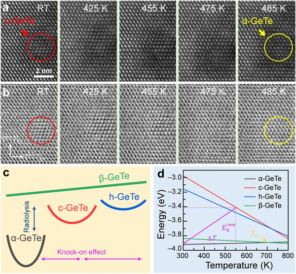
We conduct an in situ TEM heating experiment with a temperature profile given in Fig. S7 (ESI†), which allows for dynamic observation of the thermal stability of the structure formed by electron beam irradiation at the nanoscale. It can be known from the HAADF- and simultaneously recorded ABF-STEM images in Fig. 4a and b that, with increasing temperature, c-GeTe in the ROI is thermally stable until 475 K, which transforms into α-GeTe when the temperature is above 485 K. It should be noted that the color circles indicate the ROI in Fig. 4a and b. Such an Arrhenius barrier of ∼200 K is proposed to compensate for the knock-on effect due to 200 s electron beam irradiation, as illustrated in Fig. 4c. DFT calculation is performed to explain the polymorphic phase transformation from an energetic perspective. It should be noted that both c-GeTe and h-GeTe are coherently embedded in the α-GeTe matrix as shown in Fig. 2. Additionally, the lattice parameters of α-GeTe (a = 4.170(1) Å and c = 10.672(9) Å) were obtained from the XRD results in Fig. 1b. Based on the crystallographic OR between α-GeTe and c-GeTe (or h-GeTe), the lattice parameters are calculated to be a = 5.900 Å for c-GeTe, and a = 4.172 Å and c = 20.438 Å for h-GeTe. We determine the linear thermal expansion parameters based on MD simulations, which are 1.8 × 10⁻⁵ K−1, 7.1 × 10⁻⁶ K−1, 9.8 × 10⁻⁶ K−1, and 3.4 × 10⁻⁵ K−1 for α-GeTe, c-GeTe, h-GeTe, and β-GeTe, respectively. The calculated temperature-dependent energies per atom are plotted in Fig. 4d, being consistent with Fig. 4a–c.
To understand the electronic transport characteristics, which govern macroscopic physical and chemical fundamentals, we calculate the band structure and density-of-state (DOS) of different phases of GeTe using the DFT method. As shown in Fig. 5a–d, α-GeTe is a wide-gap semiconductor, with a direct bandgap (Eg) at the L point being ∼0.6 eV. The conduction band minimum (CBM) is comprised of the Ge_4p2 state, while the valence band maximum (VBM) is occupied by the Te_5p4 state. Trackable contribution from the Ge_4s2 state near the VBM indicates the hybridization of Te_5p4 orbitals and Ge_4s2 lone pairs, which dominates the hole transport given that α-GeTe usually has p-type conductance. In contrast, c-GeTe exhibits typical metallic characters, mainly arising from the interaction between Ge_4p2 and Te_5p4 orbitals. In terms of h-GeTe, the Te–Te vdW interaction opens an indirect Eg of ∼0.1 eV along the L-to-Γ k-path. The CBM and VBM are mainly occupied by Ge_4p2 and Te_5p4 states, corresponding to σ-type Ge–Te chemical bonds. Ultimately, β-GeTe is a narrow-gap semiconductor, with a direct Eg at the L point being ∼0.2 eV. Similar to α-GeTe, the hole transport in β-GeTe is dominated by the hybridization of Te_5p4 orbitals and Ge_4s2 lone pairs.
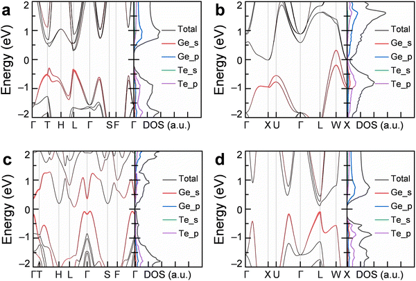 | ||
| Fig. 5 Electronic transport characteristics. (a)–(d) Band structure (left) and DOS (right) of α-GeTe, c-GeTe, h-GeTe, and β-GeTe, respectively. | ||
By comparing the constituent states of the VBM in different phases of GeTe, we believe that the polymorphic phase transformation is due to the switch of Ge_4s2 lone pairs from being quenched to being stereochemically expressed, which usually distorts its bonding with neighboring ligands. To confirm our hypothesis, we draw the fat band structure with the projected orbital weight of Ge_4s2 electrons. It is apparent that the quenching of Ge_4s2 lone pairs, viz., participating in the bonding state near the VBM, leads to the formation of resonant Ge–Te bonds in α-GeTe with ferroelectric polarization and β-GeTe with anisotropic structural dipoles.44 Whereas in c-GeTe and h-GeTe, the Ge_4s2 lone pairs tend to express themself due to a decrease in the coordination number of Ge from 6 to 4, leading to the formation of these two metastable phases.
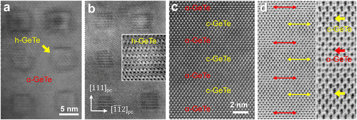
The polymorphic phase transformation inspires us to carry out an electron beam lithography study, which can be used to pattern the motifs of c-GeTe and/or h-GeTe in α-GeTe.45–48 As displayed in Fig. 6a and b, the HAADF- and ABF-STEM images show the as-fabricated 3 × 2 nanopillars of h-GeTe embedded in the α-GeTe matrix. Such a system can be regarded as a proof-of-concept quantum device, containing highly dense phase boundaries and vdW gaps, accompanied by interfacial strain. According to the Debye–Callaway theory, κ of anisotropic solid materials based on the phonon relaxation time is contributed by multiple scattering processes, e.g., intrinsic normal and Umklapp phonon–phonon processes, and extrinsic scattering due to grain boundary, lattice strain, and nanoprecipitates.49,50 Hence, the formation of nanopillar arrays can effectively decrease κ and increase the figure-of-merit, which plays a prominent role in improving thermoelectric performance.
We additionally fabricated heterostructures of α-GeTe and c-GeTe superlattices using the focused electron beam. According to the HAADF- and ABF-STEM images in Fig. 6c and d, alternative α-GeTe and c-GeTe layers with coherent interfaces are stacked along the [100]pc direction. The width of each layer is ∼2 nm, being comparable with the de Broglie wavelength of electrons. This may cause quantum confinement of near-free-electron motion and surface plasmon polaritons, which are the fountain of exotic chemical and physical phenomena.51,52 It is worth mentioning that the layer width can be precisely controlled by changing the energy spread of the electron beam, making such a system competent for the application of phonoelectricity,53 thermoionicity,54 photoelectricity,55etc.
Conclusions
In summary, we observe the previously unreported phases of c-GeTe and h-GeTe, which enter into a controllable polymorphic phase transformation via electron beam irradiation. With aberration-corrected STEM characterization, c-GeTe is resolved as in a sphalerite structure, while h-GeTe is resolved as in a rhombohedral structure with vdW gaps. In situ heating experiments imply that c-GeTe is thermally stable at 475 K, which is consistent with MD simulations. The electronic transport characteristics of all phases of GeTe are rationalized using DFT calculations, and are sensitive to the bonding state of Ge_4s2 lone pairs. Most importantly, we demonstrate that the focused high-energy electron beam can be used for patterning nanopillars and superlattices of c-GeTe and h-GeTe in the α-GeTe matrix, providing a strategic approach for fabricating quantum devices to broaden the application scope of IV–VI chalcogenides.Experimental
Material synthesis
GeTe samples with a nominal composition of Ge0.5 Te0.5 (at%) are synthesized through a traditional solidification process. Ge and Te powders in trace-metal purity are weighed out according to stoichiometry and hand-ground with a mortar and pestle in an argon-filled glove box. The mixed products are sealed in fused quartz tubes under vacuum (<5 Pa), followed by heating to 1173 K at 5 K min−1 and kept at this temperature for 10 h. After that, the molten products are quickly cooled to room temperature to form highly dense ingot samples.Characterization
Phase analyses are performed by X-ray diffraction (XRD, Rigaku D/Max-2400) with Cu-Kα (λ = 1.5418 Å) radiation. Surface morphology is characterized using a scanning electron microscope (SEM, FEI Quanta FEG 250) with a secondary electron (SE) detector. Transmission electron microscopy specimens are prepared by mechanical thinning, followed by argon ion milling on a stage cooled by liquid nitrogen. In situ heating STEM specimens are prepared by the focused ion beam (FIB, Thermos Fisher Helios NanoLab 600i) lift-out technique. The diffraction contrast images, SAED, HAADF, and ABF images are collected by a TEM and a STEM using the JEOL ARM200F equipped with a probe aberration corrector, and HAADF- and ABF-STEM detectors covering the angular ranges of 90–176 and 11–23 mrad, respectively. It should be noted that the in situ experiment is performed on the DENSsolution heating specimen holder in the STEM. The simulated HAADF-STEM images are obtained based on the multi-slice method.54DFT calculations
DFT calculations and molecular dynamics (MD) simulations in the canonical ensemble (N, V, and T) are performed using a projector-augmented wave (PAW) method as implemented in the Vienna Ab initio Simulation Package (VASP).56–59 Fully relativistic Perdew–Burke–Ernzerhof generalized gradient approximation functional (GGA-PBE) is adopted to treat the exchange–correlation interaction.60 A 21 × 21 × 21 Monkhorst–Pack k-mesh is created to sample the primitive cells of different phases of GeTe for structural relaxation with a plane wave cut-off energy of 500 eV. The convergence criterion is set to be 1 × 10⁻⁷ eV per electron and 1 × 10⁻³ eV Å−1 per atom. The spin–orbital coupling (SOC) effect is considered because Te is a heavy element. The electron band structures are calculated along the line-mode k-path based on Brillouin path features indicated by the AFLOW framework.61Author contributions
H. Z.: investigation, formal analysis, and writing – original draft. M. L.: investigation, data curation, and writing – original draft. S. M.: supervision, conceptualization, funding acquisition, and writing – review and editing. S. C.: methodology and walidation. L. L.: formal analysis and walidation. Z. C.: supervision, funding acquisition, and writing – review and editing.Data availability
The data are available from the corresponding author on reasonable request.Conflicts of interest
There are no conflicts to declare.Acknowledgements
This work is financially supported by the Basic and Applied Basic Research Major Programme of Guangdong Province, China (Grant No. 2021B0301030003), and Ji Hua Laboratory Project (Grant No. X210141TL210). Z.-G. Chen thanks the financial support from the Australian Research Council, HBIS-UQ Innovation Centre for Sustainable Steel project, and QUT Capacity Building Professor Program. The authors acknowledge the Research Computing Centre at the Queensland University of Technology and National Computational Infrastructure supported by the Australian Government for providing computing resources and support.Notes and references
- L. Perniola, V. Sousa, A. Fantini, E. Arbaoui, A. Bastard, M. Armand, A. Fargeix, C. Jahan, J. F. Nodin, A. Persico, D. Blachier, A. Toffoli, S. Loubriat, E. Gourvest, G. B. Beneventi, H. Feldis, S. Maitrejean, S. Lhostis, A. Roule, O. Cueto, G. Reimbold, L. Poupinet, T. Billon, B. D. Salvo, D. Bensahel, P. Mazoyer, R. Annunziata, P. Zuliani and F. Boulanger, IEEE Electron Device Lett., 2010, 31, 488–490 CAS.
- G. Bruns, P. Merkelbach, C. Schlockermann, M. Salinga, M. Wuttig, T. D. Happ, J. B. Philipp and M. Kund, Appl. Phys. Lett., 2009, 95 Search PubMed.
- M. Terao, T. Morikawa and T. Ohta, Jpn. J. Appl. Phys., 2009, 48, 080001 CrossRef.
- P. Bauer Pereira, I. Sergueev, S. Gorsse, J. Dadda, E. Müller and R. P. Hermann, Phys. Status Solidi B, 2013, 250, 1300–1307 CrossRef CAS.
- K. Shportko, S. Kremers, M. Woda, D. Lencer, J. Robertson and M. Wuttig, Nat. Mater., 2008, 7, 653–658 CrossRef CAS.
- M. Hong, M. Li, Y. Wang, X.-L. Shi and Z.-G. Chen, Adv. Mater., 2023, 35, 2208272 CrossRef CAS.
- X. Zhang, Z. Bu, S. Lin, Z. Chen, W. Li and Y. Pei, Joule, 2020, 4, 986–1003 CrossRef CAS.
- T. Xing, Q. Song, P. Qiu, Q. Zhang, X. Xia, J. Liao, R. Liu, H. Huang, J. Yang, S. Bai, D. Ren, X. Shi and L. Chen, Nat. Sci. Rev., 2019, 6, 944–954 CrossRef CAS PubMed.
- D. Wu, L. Xie, X. Xu and J. He, Adv. Funct. Mater., 2019, 29, 1806613 CrossRef.
- S. Varotto, L. Nessi, S. Cecchi, J. Sławińska, P. Noël, S. Petrò, F. Fagiani, A. Novati, M. Cantoni, D. Petti, E. Albisetti, M. Costa, R. Calarco, M. Buongiorno Nardelli, M. Bibes, S. Picozzi, J.-P. Attané, L. Vila, R. Bertacco and C. Rinaldi, Nat. Electron., 2021, 4, 740–747 CrossRef CAS.
- D. Kriegner, G. Springholz, C. Richter, N. Pilet, E. Müller, M. Capron, H. Berger, V. Holý, J. H. Dil and J. Krempaský, Crystals, 2019, 9, 335 CrossRef CAS.
- X. Wang, L. Zhou, J. Feng, S. Wang, H. Qian, H. Tong and X.-S. Miao, Appl. Phys. Lett., 2018, 113, 232903 CrossRef.
- D. Lencer, M. Salinga and M. Wuttig, Adv. Mater., 2011, 23, 2030–2058 CrossRef CAS.
- R. A. Hein, J. W. Gibson, R. Mazelsky, R. C. Miller and J. K. Hulm, Phys. Rev. Lett., 1964, 12, 320–322 CrossRef CAS.
- S. Raoux, H.-Y. Cheng, M. A. Caldwell and H.-S. P. Wong, Appl. Phys. Lett., 2009, 95, 071910 CrossRef.
- S. Perumal, S. Roychowdhury and K. Biswas, J. Mater. Chem. C, 2016, 4, 7520–7536 RSC.
- M. Zhu, O. Cojocaru-Mirédin, A. M. Mio, J. Keutgen, M. Küpers, Y. Yu, J.-Y. Cho, R. Dronskowski and M. Wuttig, Adv. Mater., 2018, 30, 1706735 CrossRef.
- T. Chattopadhyay, J. X. Boucherle and H. G. vonSchnering, J. Phys. C: Solid State Phys., 1987, 20, 1431 CrossRef CAS.
- B. J. Kooi and M. Wuttig, Adv. Mater., 2020, 32, 1908302 CrossRef CAS.
- J. E. Boschker, R. Wang and R. Calarco, CrystEngComm, 2017, 19, 5324–5335 RSC.
- A. Onodera, I. Sakamoto, Y. Fujii, N. Mo⁁ri and S. Sugai, Phys. Rev. B: Condens. Matter Mater. Phys., 1997, 56, 7935–7941 CrossRef CAS.
- K. Jeong, H. Lee, C. Lee, L. H. Wook, H. Kim, E. Lee and M.-H. Cho, Appl. Mater. Today, 2021, 24, 101122 CrossRef.
- D. Dangic, O. Hellman, S. Fahy and I. Savic, npj Comput. Mater., 2021, 7, 57 CrossRef CAS.
- M. Xu, Z. Lei, J. Yuan, K. Xue, Y. Guo, S. Wang, X. Miao and R. Mazzarello, RSC Adv., 2018, 8, 17435–17442 RSC.
- P. M. Konze, V. L. Deringer and R. Dronskowski, Chem. Mater., 2016, 28, 6682–6688 CrossRef CAS.
- A. Frolov, J. Sánchez-Barriga, C. Callaert, J. Hadermann, A. Fedorov, D. Usachov, A. Chaika, B. Walls, K. Zhussupbekov, I. Shvets, M. Muntwiler, M. Amati, L. Gregoratti, A. Varykhalov, O. Rader and L. Yashina, ACS Nano, 2020, 14(12), 16576–16589 CrossRef CAS.
- H. S. Lee, B.-S. Kim, C.-W. Cho, M.-W. Oh, B.-K. Min, S.-D. Park and H.-W. Lee, Acta Mater., 2015, 91, 83–90 CrossRef CAS.
- K. Jeong, S. Park, D. Park, M. Ahn, J. Han, W. Yang, H.-S. Jeong and M.-H. Cho, Sci. Rep., 2017, 7, 955 CrossRef.
- V. V. Ionin, A. V. Kiselev, N. N. Eliseev, V. A. Mikhalevsky, M. A. Pankov and A. A. Lotin, Appl. Phys. Lett., 2020, 117, 011901 CrossRef CAS.
- T.-T. Jiang, X.-D. Wang, J.-J. Wang, Y.-X. Zhou, D.-L. Zhang, L. Lu, C.-L. Jia, M. Wuttig, R. Mazzarello and W. Zhang, Acta Mater., 2020, 187, 103–111 CrossRef CAS.
- T. Siegrist, P. Jost, H. Volker, M. Woda, P. Merkelbach, C. Schlockermann and M. Wuttig, Nat. Mater., 2011, 10, 202–208 CrossRef CAS.
- V. Bragaglia, F. Arciprete, W. Zhang, A. M. Mio, E. Zallo, K. Perumal, A. Giussani, S. Cecchi, J. E. Boschker, H. Riechert, S. Privitera, E. Rimini, R. Mazzarello and R. Calarco, Sci. Rep., 2016, 6, 23843 CrossRef CAS.
- K. S. Siegert, F. R. L. Lange, E. R. Sittner, H. Volker, C. Schlockermann, T. Siegrist and M. Wuttig, Rep. Prog. Phys., 2015, 78, 013001 CrossRef CAS PubMed.
- P. D. Nellist, M. F. Chisholm, A. R. Lupini, A. Borisevich, J. W. H. Sides, S. J. Pennycook, N. Dellby, R. Keyse, O. L. Krivanek, M. F. Murfitt and Z. S. Szilagyi, J. Phys. Conf. Ser., 2006, 26, 7 CrossRef.
- S. D. Findlay, N. Shibata, H. Sawada, E. Okunishi, Y. Kondo and Y. Ikuhara, Ultramicroscopy, 2010, 110, 903–923 CrossRef CAS PubMed.
- I. E. Dzyaloshinskii, E. M. Lifshitz and P. P. Lev, Soviet Physics - Uspekhi, 1961, 4, 153 CrossRef.
- X. Qu and Q. Deng, RSC Adv., 2017, 7, 37032–37038 RSC.
- D. Wu, D. Feng, X. Xu, M. He, J. Xu and J. He, J. Alloys Compd., 2019, 805, 831–839 CrossRef CAS.
- V. V. Ionin, A. V. Kiselev, A. A. Burtsev, V. A. Mikhalevsky, N. N. Eliseev, I. M. Asharchuk, V. I. Sokolov and A. A. Lotin, Appl. Phys. Lett., 2021, 119, 081105 CrossRef CAS.
- R. F. Egerton, R. McLeod, F. Wang and M. Malac, Ultramicroscopy, 2010, 110, 991–997 CrossRef CAS.
- F. J. Bryant, A. F. J. Cox and F. C. Frank, Proc. R. Soc. Edinburgh, Sect. A: Math. Phys. Sci., 1969, 310, 319–339 CAS.
- Y. Kudriavtsev, A. Villegas, A. Godines and R. Asomoza, Appl. Surf. Sci., 2005, 239, 273–278 CrossRef CAS.
- Y. Tu, L. Xie, S. J. Pennycook, M. Bosman and J. Q. He, Sci. Adv., 2022, 8, eadd7690 CrossRef PubMed.
- W. G. Zeier, A. Zevalkink, Z. M. Gibbs, G. Hautier, M. G. Kanatzidis and G. J. Snyder, Angew. Chem., Int. Ed., 2016, 55, 6826–6841 CrossRef CAS PubMed.
- S. Kim, S. Jung, J. Lee, S. Kim and A. G. Fedorov, ACS Appl. Mater. Interfaces, 2020, 12, 39595–39601 CrossRef CAS.
- S. Jesse, Q. He, A. R. Lupini, D. N. Leonard, M. P. Oxley, O. Ovchinnikov, R. R. Unocic, A. Tselev, M. Fuentes-Cabrera, B. G. Sumpter, S. J. Pennycook, S. V. Kalinin and A. Y. Borisevich, Small, 2015, 11, 5895–5900 CrossRef CAS PubMed.
- R. R. Unocic, A. R. Lupini, A. Y. Borisevich, D. A. Cullen, S. V. Kalinin and S. Jesse, Nanoscale, 2016, 8, 15581–15588 RSC.
- L. Yao, S. Majumdar, L. Äkäslompolo, S. Inkinen, Q. H. Qin and S. van Dijken, Adv. Mater., 2014, 26, 2789–2793 CrossRef CAS.
- P. G. Klemens, Proc. R. Soc. Edinburgh, Sect. A: Math., 1955, 68, 1113 CrossRef.
- J. Yang, L. Xi, W. Qiu, L. Wu, X. Shi, L. Chen, J. Yang, W. Zhang, C. Uher and D. J. Singh, npj Comput. Mater., 2016, 2, 15015 CrossRef CAS.
- P. Bharadwaj, A. Bouhelier and L. Novotny, Phys. Rev. Lett., 2011, 106, 226802 CrossRef.
- C. Melnick and M. Kaviany, Appl. Phys. Rev., 2019, 6, 021305 Search PubMed.
- C. Herring and M. H. Nichols, Rev. Modern Phys., 1949, 21, 185–270 CrossRef CAS.
- E. O. Kane, Phys. Rev., 1962, 127, 131–141 CrossRef CAS.
- J. M. LeBeau, S. D. Findlay, L. J. Allen and S. Stemmer, Phys. Rev. Lett., 2008, 100, 206101 CrossRef PubMed.
- G. Kresse and J. Hafner, J. Phys.: Condens. Matter, 1994, 6, 8245 CrossRef CAS.
- G. Kresse and J. Hafner, Phys. Rev. B: Condens. Matter Mater. Phys., 1993, 47, 558–561 CrossRef CAS.
- G. Kresse and J. Furthmüller, Phys. Rev. B: Condens. Matter Mater. Phys., 1996, 54, 11169–11186 CrossRef CAS.
- G. Kresse and D. Joubert, Phys. Rev. B: Condens. Matter Mater. Phys., 1999, 59, 1758–1775 CrossRef CAS.
- J. P. Perdew, K. Burke and M. Ernzerhof, Phys. Rev. Lett., 1996, 77, 3865–3868 CrossRef CAS.
- W. Setyawan and S. Curtarolo, Comput. Mater. Sci., 2010, 49, 299–312 CrossRef.
Footnotes |
| † Electronic supplementary information (ESI) available. See DOI: https://doi.org/10.1039/d4nh00035h |
| ‡ These authors contributed equally. |
| This journal is © The Royal Society of Chemistry 2024 |

