
Surface-enhanced optical-mid-infrared photothermal microscopy using shortened colloidal silver nanowires: a noble approach for mid-infrared surface sensing†
Naoki
Baden
a,
Hirohmi
Watanabe
b,
Masaru
Aoyagi
b,
Hiroshi
Ujii
cde and
Yasuhiko
Fujita
 *b
*b
aNihon Thermal Consulting, Co., Ltd, 3-9-2 Nishishinjuku, Sinjuku-ku, Tokyo 160-0023, Japan
bResearch Institute for Sustainable Chemistry, National Institute of Advanced Industrial Science and Technology (AIST), Kagamiyama 3-11-32, Higashihiroshima, Hiroshima 739-0046, Japan. E-mail: yasuhiko.fujita@aist.go.jp
cResearch Institute for Electronic Science (RIES) and Division of Information Science and Technology, Graduate School of Information Science and Technology, Hokkaido University, N20W10, Sapporo, Hokkaido 001-0020, Japan
dDepartment of Chemistry, Division of Molecular Imaging and Photonics, KU Leuven, Celestijnenlaan 200F, B-3001 Leuven, Belgium
eInstitute for Integrated Cell-Material Science (WPI-iCeMS), Kyoto University, Yoshida, Sakyo-ku, Kyoto 606-8501, Japan
First published on 23rd May 2024
Abstract
We propose surface-enhanced optical-mid-infrared photothermal (MIP) microscopy using highly crystalline silver nanowires, acting as a Fabry–Perot resonator, and demonstrate its applicability to enhanced mid-infrared surface sensing of thin polymer layers as thin as 20 nm.
New conceptsThis paper presents a novel approach in optical-mid-infrared photothermal (MIP) microscopy that enables surface sensing of polymer top surfaces with a depth resolution below 20 nm. Highly crystalline silver nanowires were deposited directly onto the polymer surfaces, and by measuring polarized optical-MIP spectra at the silver nanowire, a chemical fingerprint of the top surfaces of the sample can be obtained through the resonant-surface-enhanced infrared absorption (SEIRA) effect. Silver nanowires of several μm in length can be produced by a simple ultrasonic treatment of the original long nanowires available on the market. These shortened silver nanowires were found to serve as a strong mid-IR plasmonic antenna, and their resonant frequency can be fine-tuned by their length. Furthermore, by averaging optical-MIP spectra with multiple nanowires of different lengths, a broad infrared resonance can be achieved across the IR fingerprint region. Finally, an improved optical-MIP surface sensitivity is presented in a hydrolyzed polyimide layer as thin as 20 nm. |
Mid-infrared photothermal (MIP) microscopy is one of the most advanced super-resolution infrared techniques available today. When pulsed infrared light is directed at samples, it induces a photothermal response through infrared (IR) absorption by the sample. This results in a small change in the physical properties of the sample, such as thermal expansion, pressure wave emission, refractive index, and/or Grüneisen parameter.1 These changes can be detected using either the AFM cantilever or focused visible light, effectively overcoming the diffraction limit of IR light. The former AFM-type, commonly known as AFM-IR or AFM-PTIR, was launched in 2010 by Anasys Instruments (now Bruker). This technology has demonstrated the spatial resolution of less than 50 nm in both the lateral and depth directions.2,3 Achieving such high resolution is facilitated by the frequency mixing, notably in tapping AFM-IR.4,5 Concurrently, an optical-type MIP system, designed as an optical-photothermal infrared (O-PTIR) microscopy system, was developed and commercialized in 2018 (mIRage, Photothermal Spectroscopy Corp.). This optical-MIP has rapidly gained popularity due to its ease of use and versatility in both air and aqueous environments.6 As a result, there has been a significant increase in its applications, ranging from material sciences7–9 to life sciences,10–12 including live MIP imaging beyond video rate.13–15 While optical-MIP microscopy provides a lateral resolution in the range of several hundred nm, the surface sensitivity (i.e. depth resolution) is limited to a few μm.16 This limitation is due to the large penetration depth of mid-IR light, which is a major challenge in current optical-MIP microscopy, apart from AFM-IR.
One approach to improve the sensitivity of vibrational spectroscopy is the use of surface plasmons. In the visible range, direct light irradiation to noble metal nanostructures leads to collective oscillations of electrons in metals, called localized surface plasmon resonances (LSPRs). LSPRs produce strong near-field light that decays exponentially with distance from the metal surface. Enormous efforts have been made to strategically exploit the near-field for spectroscopic applications, from molecular sensing of analytes in solution17,18 to surface sensing of bulk samples19,20 (e.g. SERS stamps), each taking advantage of the improved detection sensitivity and depth resolution provided by LSPRs. Wet-synthesized, highly crystalline colloidal metal nanostructures have been actively incorporated for these purposes due to their low ohmic damping nature.17,18
In the mid-IR region, however, direct excitation of LSPRs by far-field light is not feasible due to the large negative permittivity of noble metals. Noble metal nanospheres, often used in visible plasmonics, are not feasible for mid-IR plasmonic applications. Therefore, an analogy of a dipole antenna is applied to excite plasmons.21 A simple yet highly effective antenna structure is a noble metal nanowire. Light irradiation to such nanowires gives rise to collective oscillations of electrons via cavity resonances (e.g. Fabry–Perot resonances), which induces the plasmonic near-field. This near-field has been shown to effectively enhance the mid-IR absorption coefficiency of surrounding molecules, called resonant surface-enhanced IR absorption (resonant-SEIRA).21 Since the pioneering work by Neubrech et al.,22 extensive studies have been carried out on the view of resonance tuning,22–28 spatial scaling,29–31 sensitivity,24,25,27,32,33 antenna shape,25,26,30,33–36 and plasmonic materials.37–39 The resonant antenna structures are often fabricated by a top-down approach, such as electron beam lithography,23–26,29–33,35,40–43 for the artificial design of sub-wavelength (periodic) structures. Resonant-SEIRA has been applied to molecular sensing of analytes, including gas molecules,44 biomolecules,24,30,32,37 or their in situ monitoring.27,45
A drawback of the current SEIRA platform is the need to deliver analytes to the plasmonic (periodic) substrate, often requiring ensemble measurements to obtain sufficient IR signals. Potentially, wet-synthesized, colloidal noble metal nanowires could open up the possibility of versatile surface sensing on any surface due to their flexibility in structure positioning. In addition, the highly crystalline nature of the colloidal metal nanowires would allow resonant-SEIRA measurements down to the single nanowire level, as recently demonstrated by Li et al.28 However, there are only a few publications using colloidal metal nanostructures in SEIRA applications,28,36,46–49 and, to the best of our knowledge, a versatile SEIRA approach that is capable of obtaining chemical fingerprints on arbitrary bulk surfaces has not yet been reported.
Here, we propose surface-enhanced optical-MIP microscopy using a wet-synthesized silver nanowire antenna as a versatile surface sensing platform. We report that highly crystalline, shortened silver nanowires of several μm-length, which act as a Fabry–Perot resonator, can be easily fabricated by a simple ultrasonic treatment of a solution containing long chemically synthesized silver nanowires of 10–30 μm lengths. Our strategy for MIP surface sensing is straightforward: disperse shortened silver nanowires directly onto arbitrary surfaces and measure spectra at the nanowires with the desired resonance frequency. In this context, we have investigated the mid-IR antenna activity of silver nanowires both experimentally and with numerical simulations. Finally, we demonstrate surface-sensitive infrared detection on polymer samples, achieving a 10-fold increase in detection sensitivity compared to conventional optical-MIP microscopy, and improved surface sensitivity (i.e. depth resolution) down to below 20 nm.
Fig. 1(a) shows a schematic of a reflection-type MIP (O-PTIR) system (mIRageTM, Photothermal Spectroscopy Corp.) used in this study. Wavelength-tunable pulsed IR laser light from a quantum cascade laser (QCL) was focused on a nanowire/sample using a Cassegrain objective lens (40×, 0.78 N.A.). Pulsed IR irradiation induces a photothermal response of the sample system via either the Fabry–Perot resonance of the nanowire or the IR absorption of the sample. This instant response was lock-in detected by a change in reflectance of a co-focused 532 nm continuous wave laser, the magnitude of which is known to be proportional to the IR absorption coefficient.16,50
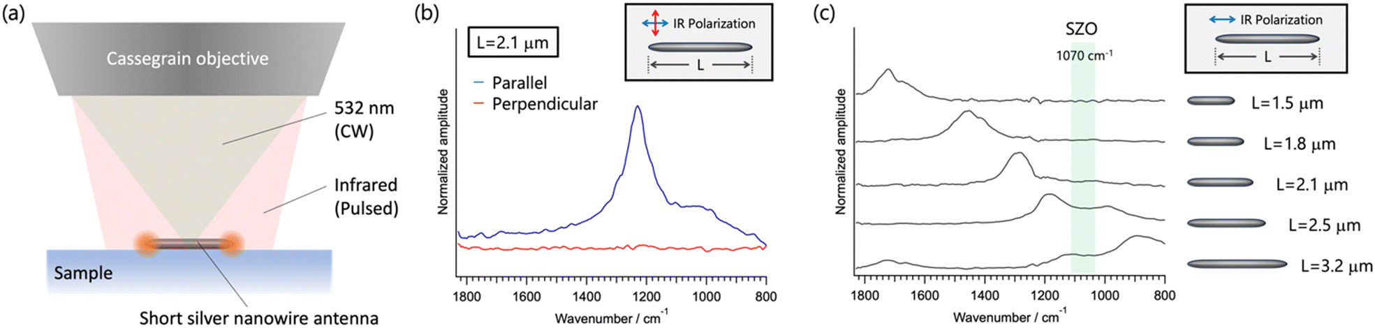 | ||
| Fig. 1 (a) Schematic illustration of surface-enhanced optical-mid infrared photothermal (MIP) microscopy using a resonant short silver nanowire antenna. (b) Optical-MIP spectra obtained on silver nanowire (L = 2.1 μm)/low-e glass with infrared polarization set to parallel (blue) and perpendicular (red) to the long axis of the nanowire. (c) Optical-MIP spectra of silver nanowires on low-e glass with the nanowire length (L) of L = 1.5–3.2 μm. The IR polarization was set to be parallel to the long axis of the nanowire. | ||
We performed MIP measurements on three sample systems: (1) a silver nanowire/low-e glass system, (2) a silver nanowire/polystyrene/glass system, and (3) a nanowire/poly(amic acid)/polyimide system. The first system of (1) was used to study the length-dependence of the plasmon resonance of silver nanowire antennas. The latter (2) and (3) aimed to demonstrate the enhanced MIP sensitivity by the nanowire antenna. In both systems, the original silver nanowire (Sigma-Aldrich, d = 105 nm (d: diameter) on average, see Fig. S1, ESI†) was ultrasonicated before being spin-cast onto the surfaces. The used silver nanowires are reported to be synthesized by the polyol method and surfactant molecules of polyvinylpyrrolidone (PVP) cover the entire silver surfaces.51 The ultrasonic treatment was continued until the desired nanowire lengths were obtained. In particular, under our experimental conditions, the ultrasonic treatment for 3 h resulted in the production of silver nanowires of several μm in length (Fig. S2, ESI†), in which the resonance frequency of the first (m = 1) to third (m = 3) order longitudinal plasmon modes matches with the IR fingerprint region (i.e. 800–1850 cm−1). Note that no further treatment to remove PVPs was performed in this study.
First, an experimental investigation into the IR resonance of silver nanowires was carried out. For this purpose, the shortened silver nanowires were spin-cast on low-emissivity (low-e) glass (MirrIR, Kevley Technologies, Chesterland, OH, USA). The low-e glass has a thin coating of three layers of Ag + SZO (Sn-doped Zinc Oxide) on top of a glass substrate, which reflects over 90% of IR light in the mid-IR region (Fig. S3, ESI†). In Fig. 1(b), the MIP spectrum of a single 2.1 μm-length single silver nanowire deposited on low-e glass is presented, obtained with two different IR polarization directions. Note that 532 nm probe light was focused at the center of the nanowire, with a spot size of approximately 1 μm in diameter. Parallel excitation (i.e. irradiation of a focused IR beam with polarization parallel to the longitudinal axis of the nanowire) resulted in a broad peak at ∼1240 cm−1, while perpendicular excitation showed no IR response, indicating a strong polarization dependence of the nanowire antenna. The absence of PVP peaks in the MIP spectra may be below the detection limit. Fig. 1(c) shows optical-MIP spectra obtained on single silver nanowires of five different lengths under parallel excitation. It clearly shows that the resonance peak, which can be attributed to a fundamental cavity plasmon mode (m = 1, Fig. S4, ESI†), shifts to a lower wavenumber with increasing nanowire length, in agreement with previous reports on lithography-fabricated gold nanowires.7 The nanowire with L = 3.2 μm shows, in addition to the m = 1 peak at around 880 cm−1, another peak at around 1700 cm−1, representing a higher order plasmon mode. Interestingly, a decrease in peak intensity was observed in the spectra at the frequency corresponding to SZO absorption at around 1070 cm−1 (e.g. L = 2.5, 3.2 μm). This intensity decrease may be attributed to the strong light-matter coupling between cavity-plasmons and SZO. Therefore, it is likely that shortened silver nanowires act as strong Fabry–Perot plasmonic antennas.
We then performed a finite-difference time-domain (FDTD) simulation to gain further insight into the plasmon resonance modes. Fig. 2(a) shows a plot of the E-field intensity as a function of wavenumber, along with a corresponding E-field intensity distribution image at each peak (Fig. 2(b)). The silver nanowire was modelled as a cylindrical structure with L = 2.5 μm and d = 100 nm (details of the FDTD calculations can be found in ESI†). The silver nanowire showed 3 peaks at 1500, 4600, and 7700 cm−1, corresponding to m = 1, m = 3, and m = 5 resonances, respectively, according to the E-field images. Fig. 2(c) illustrates the E-field intensity as a function of nanowire length and wavenumber, and shows that both m = 1 and m = 3 resonances shift to a lower frequency as the nanowire length increases. In addition, the m = 1 mode was found to be the most intense in the E-field intensity and to cover the widest wavenumber range in E-field enhancement among other higher modes (Fig. S5, ESI†). This suggests that the use of m = 1 can benefit infrared applications in terms of strong signal enhancement over a broad frequency range in a single nanowire system. Fig. 2(d) represents the experimental results plotted in the same manner as Fig. 2(c), with the scale range corresponding to the grey box in Fig. 2(c). According to the previous reports,7,52,53 not only the odd modes but also the even modes can potentially be excited with the used mid-IR angle of incidence (NA = 0.8), while we observe only the odd modes. A possible reason for the absence of the even mode (m = 2) in our experiment could be that the resonance of the even modes is relatively weaker than that of the odd modes, since only a limited fraction of the incident photons can excite the even modes. As a result, the MIP signals from the even modes were below the sensitivity limit. Nonetheless, as can be seen from the plot, the experiment essentially showed good agreement with the simulation, highlighting the fine tunability of plasmon resonance by silver nanowire structures. A small variation of the resonance positions in Fig. 2(d) could be due to the variation of the nanowire widths (Fig. S1, ESI†).
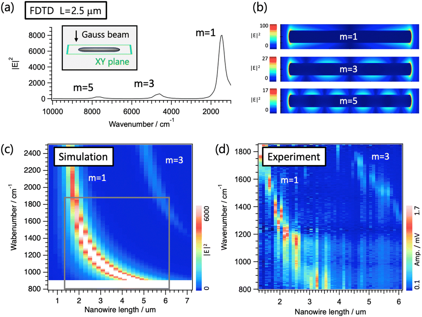 | ||
| Fig. 2 (a) A simulated E-field intensity spectrum of a silver nanowire (length L = 2.5 μm, diameter d = 100 nm) and (b) corresponding E-field distribution maps at m = 1, 3, and 5. (c) and (d) Plots of E-field intensity as a function of wavenumber and nanowire length obtained by simulation (c) and experiment (d). | ||
Next, the enhancement of the MIP sensitivity by silver nanowires in a thin PS film on glass was demonstrated. Fig. 3(a)–(c) show optical-MIP spectra of PS/glass with (blue) and without (black) silver nanowires, with the PS thickness tuned to 40, 160, and 1000 nm, respectively. IR peaks at 1492, 1450, and 1050 cm−1 (broad) are assigned to phenyl C![[double bond, length as m-dash]](https://www.rsc.org/images/entities/char_e001.gif) C stretching (PS), CH bending (PS), and Si–O stretching (Glass), respectively. The broad background enhancement observed in the presence of the nanowire can be attributed to the IR resonance (=absorption) of the nanowire. The thickness of the spin-cast PS layer was controlled by the concentration of the PS/toluene solution and was confirmed by a laser microscope at the scratched region with a depth resolution of 5 nm. The spectrum of ‘with nanowire’ was obtained by averaging three spectra measured on silver nanowires with L = 1.8, 2.3, and 2.7 μm under the parallel excitation (spectra before averaging are shown in Fig. S6, ESI†). This averaging process allows a broad range of surface-enhanced MIP spectra to be obtained from 1000–1800 cm−1. Without nanowires, as the PS thickness decreased, the PS peaks at 1450 and 1492 cm−1 weakened and became almost negligible at 40 nm PS thickness because the sensitivity of the MIP system used was near the limit. However, with nanowires, although the PS peaks became weaker with the thinner PS films, the PS peaks can be clearly identified even with the PS thickness of 40 nm. The enhancement factor (EF), defined as the baseline-corrected peak intensity ratio with nanowire to without nanowire, was calculated for the infrared absorption of polystyrene (1492 cm−1) and glass (1050 cm−1), and then plotted as a function of PS film thickness in Fig. 3(d)–(e). The PS peak intensity was estimated by Gaussian fitting at 1492 cm−1 after linear baseline correction at 1476 to 1510 cm−1. Glass peak intensity was estimated by direct reading of the intensity at 1050 cm−1 after linear baseline correction at 850 to 1236 cm−1. The plot shows that the EF of PS remained unchanged with decreasing PS thickness up to 300 nm, but increased significantly below 100 nm PS thickness, although there was no detectable change in EF for glass. The absence of IR enhancement in the bottom glass layer suggests that strong field enhancement is confined to silver nanowires with an estimated enhancement length scale below 40 nm. These results provide a proof-of-concept for silver nanowire-based surface sensing of polymer top surfaces with a depth resolution down to 40 nm.
C stretching (PS), CH bending (PS), and Si–O stretching (Glass), respectively. The broad background enhancement observed in the presence of the nanowire can be attributed to the IR resonance (=absorption) of the nanowire. The thickness of the spin-cast PS layer was controlled by the concentration of the PS/toluene solution and was confirmed by a laser microscope at the scratched region with a depth resolution of 5 nm. The spectrum of ‘with nanowire’ was obtained by averaging three spectra measured on silver nanowires with L = 1.8, 2.3, and 2.7 μm under the parallel excitation (spectra before averaging are shown in Fig. S6, ESI†). This averaging process allows a broad range of surface-enhanced MIP spectra to be obtained from 1000–1800 cm−1. Without nanowires, as the PS thickness decreased, the PS peaks at 1450 and 1492 cm−1 weakened and became almost negligible at 40 nm PS thickness because the sensitivity of the MIP system used was near the limit. However, with nanowires, although the PS peaks became weaker with the thinner PS films, the PS peaks can be clearly identified even with the PS thickness of 40 nm. The enhancement factor (EF), defined as the baseline-corrected peak intensity ratio with nanowire to without nanowire, was calculated for the infrared absorption of polystyrene (1492 cm−1) and glass (1050 cm−1), and then plotted as a function of PS film thickness in Fig. 3(d)–(e). The PS peak intensity was estimated by Gaussian fitting at 1492 cm−1 after linear baseline correction at 1476 to 1510 cm−1. Glass peak intensity was estimated by direct reading of the intensity at 1050 cm−1 after linear baseline correction at 850 to 1236 cm−1. The plot shows that the EF of PS remained unchanged with decreasing PS thickness up to 300 nm, but increased significantly below 100 nm PS thickness, although there was no detectable change in EF for glass. The absence of IR enhancement in the bottom glass layer suggests that strong field enhancement is confined to silver nanowires with an estimated enhancement length scale below 40 nm. These results provide a proof-of-concept for silver nanowire-based surface sensing of polymer top surfaces with a depth resolution down to 40 nm.
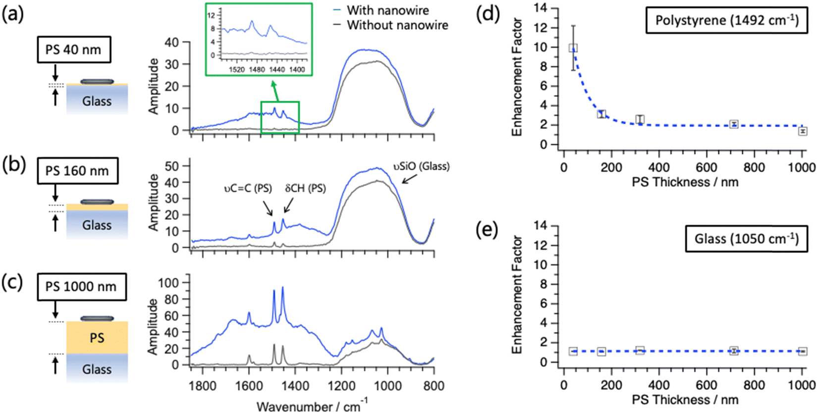 | ||
| Fig. 3 (a)–(c) Optical-MIP spectra of thin polystyrene (PS) films on glass with different PS thicknesses ((a) 40 nm, (b) 160 nm, (c) 1000 nm) obtained with (blue) and without (black) shortened silver nanowires. 1492, 1450, and 1050 cm−1 are assigned to phenyl CC stretching (PS), CH bending (PS), and Si–O stretching (Glass), respectively. (d) and (e) A plot of the enhancement factor (Inanowire/Iwithout) as a function of PS thickness at 1492 cm−1 (d) and 1050 cm−1 (e). Error bars in the plot represent standard deviations of n = 3 measurements. | ||
Finally, as a practical application example, surface-enhanced MIP detection of a thin hydrolyzed layer on a polyimide (PI) film is presented. PIs have been extensively applied to semiconductors as an interlayer dielectric for packaging,54,55 microelectromechanical systems (MEMS),55 flexible displays,56,57etc. For such applications, the chemical (and physical) properties of PI top surfaces play a critical role in the adhesion to other materials.58 While surface analysis tools, such as sum-frequency generation (SFG), X-ray photoelectron spectroscopy (XPS) or secondary ion mass spectrometry (SIMS), have been used to study soft-matter top surfaces down to 50 nm,59 a noble IR method that allows for the acquisition of such top surface chemical information would have a significant impact on science and industry.
As a model system, a PI film was alkaline-treated to form a thin, thickness-controlled hydrolyzed layer on the PI surface.60 Specifically, a commercial PI film consisting of pyromellitic dianhydride (PMDA) linked with 4,4′-oxydianiline (ODA) was immersed in 0.5 M KOH solution at 30 °C for a given reaction time ‘t’. This treatment results in the formation of a uniform hydrolyzed layer consisting of poly(amic acid) (PAA) on the film surfaces, as shown in Fig. 4(a) as an example of a cross-sectional optical microscope image (t = 400 min). As a result of hydrolysis, PAA showed characteristic IR absorption of amide I at 1650 cm−1 and amide II at 1540 cm−1, as shown in Fig. 4(b). Supplementary attenuated total reflectance-Fourier transform IR (ATR-FTIR) and AFM stiffness measurements show that the reaction proceeds at a constant kinetic rate and the thickness of the PAA layers increases linearly with the reaction time, which means that the PAA thickness can be estimated solely from the reaction time (Fig. S7, ESI†).
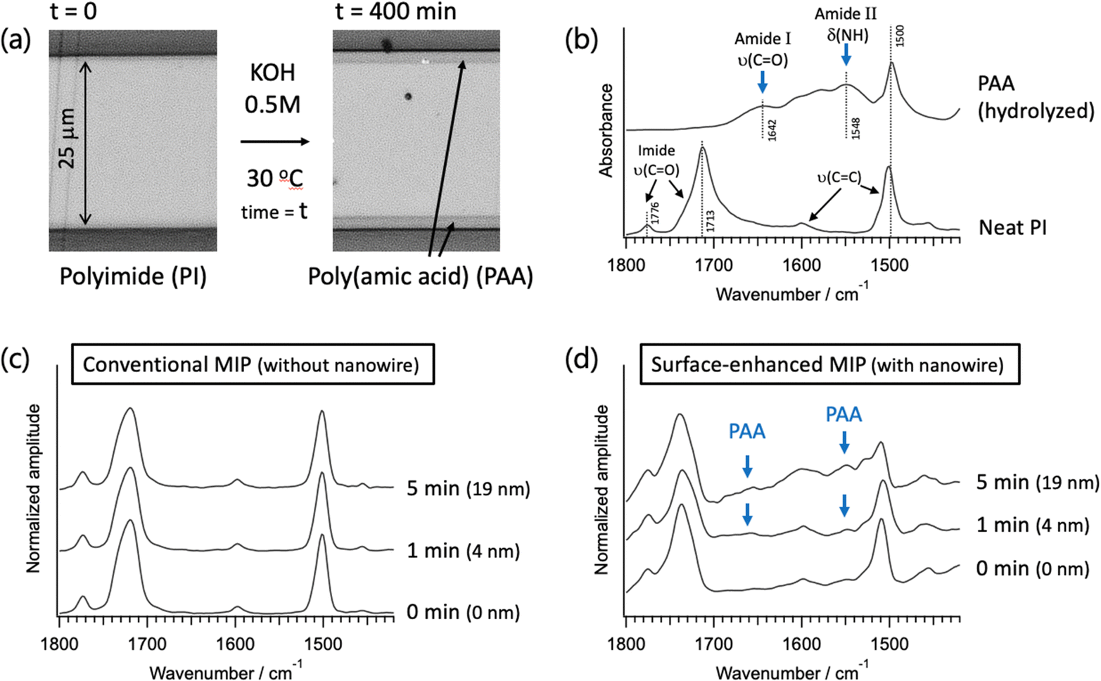 | ||
| Fig. 4 (a) Cross-sectional optical microscope images of polyimide (PI) films before (t = 0, left) and after (t = 400 min, right) KOH treatment. The thickness of the original PI film is 25 μm. The KOH treatment results in the formation of a uniform layer of poly(amic acid) (PAA) as indicated by arrows. (b) Bulk ATR-FTIR spectra of PAA (top) and neat PI. 1776 and 1713 cm−1 are assigned to the symmetric (in-phase) and antisymmetric (out-of-phase) imide CO stretching of PI. 1642 and 1548 cm−1 are assigned to the amide CO stretching and the combination of NH bending and CN stretching of PAA. For both PI and PAA, 1595 and 1500 cm−1 are assigned to benzene ring stretching. (c) and (d) Optical MIP spectra of PI films before (t = 0 min) and after (t = 1, 5 min) the KOH treatment obtained without (c) and with (d) silver nanowire. Note that the subtracted spectrum is shown for ‘with nanowire’ in (d), where the ‘without nanowire’ spectrum was subtracted from the frequency-averaged ‘with nanowire’ spectrum (Fig. S8, ESI†), to eliminate the far-field components arising from the non-nanowire region within the focal spot of the probe green light. | ||
Fig. 4(c) shows optical-MIP spectra of PI films at each reaction time without silver nanowires. Note that t = 0 min means a bare PI film. The PAA thicknesses of t = 1 min and t = 5 min samples were estimated to be 4 nm and 19 nm, respectively, according to Fig. S7(e) (ESI†). From Fig. 4(c), the characteristic IR absorption of PAA was not observed due to insufficient sensitivity, as can be expected from the results of Fig. 3. On the other hand, ‘with nanowire’ in Fig. 4(d), IR absorption assignable to both PAA and PI was observed from t = 5 min and t = 1 min samples. The ‘with nanowire’ spectrum was obtained by averaging multiple spectra measured at silver nanowires, identical to Fig. 3, and then subtracting the ‘without nanowire’ spectrum from the frequency-averaged spectrum. In Fig. 4(d), it is observed that IR absorption of PI (i.e. imide CO stretching) is still present in the spectra. This result indicates that, with such a thin PAA layer, the near-field of the nanowire not only penetrated the top PAA layer but also reached the PI bottom layer. As a result, IR signals of both PAA and PI were enhanced by the near-field. In addition, the peak positions of the antisymmetric CO stretching around 1720 cm−1 in Fig. 4(d) were shifted to a higher wavenumber compared to those in Fig. 4(c). This may indicate that the PI structure is disordered at the top surface of the neat PI film (t = 0 min) and near the interface between the PAA and PI layers (t = 1 min, 5 min), resulting in out-of-plane orientation of CO as well as disturbance of the electronic CO–N–CO conjugation.61 Nevertheless, IR absorption from the PAA layer thinner than 20 nm was successfully detected as indicated by the blue arrows in Fig. 4(d), highlighting the significant enhancement of MIP surface sensitivity by silver nanowires. Interestingly, a tiny but non-negligible PAA absorption was observed from the neat PI film (Fig. 4(d), t = 0 min). While the investigation of its origin is beyond the scope of this paper, the result insists that the neat PI film contains a trace amount of PAA components on its surfaces, which may originate from the hydrolyzed components by ambient water (e.g. moisture62), or the residue of unreacted PAA components during the film manufacturing.
To put it in perspective, combining our work with “nanowire-handling” technology, such as high-aspect nanowire synthesis,28,63 free manipulation,64,65 self-assembly,66,67 or nanowire probe fabrication,68,69 would open up a new opportunity to further generalize the method, and push the current limit of sensitivity and/or spatial resolution of both optical- and AFM-based MIP microscopy.
Conclusions
We have investigated the Fabry–Perot resonance of shortened silver nanowires and demonstrated its applicability to enhanced optical-MIP surface sensing of thin polymer layers as thin as 20 nm. We found that the chemically synthesized silver nanowires of several μm in length, produced by ultrasonication of the original long nanowires, serve as a strong mid-IR plasmonic antenna and their resonant frequency can be fine-tuned by their length. We further demonstrated that averaging optical-MIP spectra with multiple nanowires of different lengths can achieve a broad infrared resonance across the fingerprint region and improve the optical-MIP surface sensitivity down to below 20 nm.Author contributions
N. B., H. W., M. A., and Y. F. designed the experiment. H. W., M. A. and Y. F. developed experimental resources. N. B. and Y. F. conducted MIP measurements. H. U. conducted FDTD simulations. Y. F. supervised the whole project. All authors critically reviewed and revised the manuscript draft and approved the final version for submission.Conflicts of interest
The authors declare that there are no conflicts of interest regarding the publication of this article.Acknowledgements
This work was supported by JSPS KAKENHI (Grant Numbers 23K19205, 21H04634, 23H04877, 23K17856) and the Research Foundation of Flanders (FWO) research grant (G081916N, G022724N).Notes and references
- Y. R. Bai, J. Z. Yin and J. X. Cheng, Sci. Adv., 2021, 7(20), eabg1559 CrossRef CAS PubMed.
- J. Mathurin, A. Deniset-Besseau, D. Bazin, E. Dartois, M. Wagner and A. Dazzi, J. Appl. Phys., 2022, 131, 010901 CrossRef CAS.
- J. J. Schwartz, D. S. Jakob and A. Centrone, Chem. Soc. Rev., 2022, 51, 5248–5267 RSC.
- J. Mathurin, E. Pancani, A. Deniset-Besseau, K. Kjoller, C. B. Prater, R. Gref and A. Dazzi, Analyst, 2018, 143, 5940–5949 RSC.
- J. Mathurin, A. Deniset-Besseau and A. Dazzi, Acta Phys. Pol., A, 2020, 137, 29–32 CrossRef CAS.
- Q. Xia, J. Z. Yin, Z. Y. Guo and J. X. Cheng, J. Phys. Chem. B, 2022, 126, 8597–8613 CrossRef CAS PubMed.
- K. Aleshire, I. M. Pavlovetc, R. Collette, X. T. Kong, P. D. Rack, S. B. Zhang, D. J. Masiello, J. P. Camden, G. V. Hartland and M. Kuno, Proc. Natl. Acad. Sci. U. S. A., 2020, 117, 2288–2293 CrossRef CAS PubMed.
- Y. Su, X. Hu, H. J. Tang, K. Lu, H. M. Li, S. J. Liu, B. S. Xing and R. Ji, Nat. Nanotechnol., 2022, 17, 76 CrossRef CAS PubMed.
- I. M. Pavlovetc, M. C. Brennan, S. Draguta, A. Ruth, T. Moot, J. A. Christians, K. Aleshire, S. P. Harvey, S. Toso, S. U. Nanayakkara, J. Messinger, J. M. Luther and M. Kuno, ACS Energy Lett., 2020, 5, 2802–2810 CrossRef CAS.
- Y. Zhang, C. Yurdakul, A. J. Devaux, L. Wang, X. J. G. Xu, J. H. Connor, M. S. Ünlü and J. X. Cheng, Anal. Chem., 2021, 93, 4100–4107 CrossRef CAS PubMed.
- M. A. Pleitez, A. A. Khan, A. Solda, A. Chmyrov, J. Reber, F. Gasparin, M. R. Seeger, B. Schätz, S. Herzig, M. Scheideler and V. Ntziachristos, Nat. Biotechnol., 2020, 38, 293 CrossRef CAS PubMed.
- J. B. Xu, X. J. Li, Z. Y. Guo, W. E. Huang and J. X. Cheng, Anal. Chem., 2020, 92, 14459–14465 CrossRef CAS PubMed.
- G. Ishigane, K. Toda, M. Tamamitsu, H. Shimada, V. R. Badarla and T. Ideguchi, Light: Sci. Appl., 2023, 12, 174 CrossRef CAS PubMed.
- Y. R. Bai, D. L. Zhang, L. Lan, Y. M. Huang, K. Maize, A. Shakouri and J. X. Cheng, Sci. Adv., 2019, 5, eaav7127 CrossRef CAS PubMed.
- J. Z. Yin, L. Lan, Y. Zhang, H. L. Ni, Y. Y. Tan, M. Zhang, Y. R. Bai and J. X. Cheng, Nat. Commun., 2021, 12, 11 CrossRef.
- D. L. Zhang, C. Li, C. Zhang, M. N. Slipchenko, G. Eakins and J. X. Cheng, Sci. Adv., 2016, 2, e1600521 CrossRef PubMed.
- N. R. Visaveliya, R. Mazetyte-Stasinskiene and J. M. Köhler, Adv. Opt. Mater., 2022, 10, 2102757 CrossRef CAS.
- P. Mandal and B. S. Tewari, Surf. Interfaces, 2022, 28, 101655 CrossRef CAS.
- A. Nilghaz, S. M. Mousavi, A. Amiri, J. F. Tian, R. Cao and X. A. Wang, J. Agric. Food Chem., 2022, 70, 5463–5476 CrossRef CAS.
- C. C. Li, Y. M. Huang, X. Y. Li, Y. R. Zhang, Q. L. Chen, Z. W. Ye, Z. Alqarni, S. E. J. Bell and Y. K. Xu, J. Mater. Chem. C, 2021, 9, 11517–11552 RSC.
- F. Neubrech, C. Huck, K. Weber, A. Pucci and H. Giessen, Chem. Rev., 2017, 117, 5110–5145 CrossRef CAS.
- F. Neubrech, A. Pucci, T. W. Cornelius, S. Karim, A. García-Etxarri and J. Aizpurua, Phys. Rev. Lett., 2008, 101, 157403 CrossRef PubMed.
- P. Alonso-González, P. Albella, F. Neubrech, C. Huck, J. Chen, F. Golmar, F. Casanova, L. E. Hueso, A. Pucci, J. Aizpurua and R. Hillenbrand, Phys. Rev. Lett., 2013, 110, 203902 CrossRef PubMed.
- R. Adato, A. A. Yanik, J. J. Amsden, D. L. Kaplan, F. G. Omenetto, M. K. Hong, S. Erramilli and H. Altug, Proc. Natl. Acad. Sci. U. S. A., 2009, 106, 19227–19232 CrossRef CAS PubMed.
- H. Aouani, H. Sípová, M. Rahmani, M. Navarro-Cia, K. Hegnerová, J. Homola, M. H. Hong and S. A. Maier, ACS Nano, 2013, 7, 669–675 CrossRef CAS PubMed.
- I. M. Pryce, K. Aydin, Y. A. Kelaita, R. M. Briggs and H. A. Atwater, Nano Lett., 2010, 10, 4222–4227 CrossRef CAS PubMed.
- R. Adato and H. Altug, Nat. Commun., 2013, 4, 2154 CrossRef.
- N. N. Li, H. Yin, X. L. Zhuo, B. C. Yang, X. M. Zhu and J. F. Wang, Adv. Opt. Mater., 2018, 6, 1800436 CrossRef.
- D. Dregely, F. Neubrech, H. G. Duan, R. Vogelgesang and H. Giessen, Nat. Commun., 2013, 4, 2237 CrossRef PubMed.
- L. V. Brown, K. Zhao, N. King, H. Sobhani, P. Nordlander and N. J. Halas, J. Am. Chem. Soc., 2013, 135, 3688–3695 CrossRef CAS.
- P. Alonso-González, P. Albella, M. Schnell, J. Chen, F. Huth, A. García-Etxarri, F. Casanova, F. Golmar, L. Arzubiaga, L. E. Hueso, J. Aizpurua and R. Hillenbrand, Nat. Commun., 2012, 3, 684 CrossRef PubMed.
- A. De Ninno, G. Ciasca, A. Gerardino, E. Calandrini, M. Papi, M. De Spirito, A. Nucara, M. Ortolani, L. Businaro and L. Baldassarre, Phys. Chem. Chem. Phys., 2015, 17, 21337–21342 RSC.
- I. M. Pryce, Y. A. Kelaita, K. Aydin and H. A. Atwater, ACS Nano, 2011, 5, 8167–8174 CrossRef CAS PubMed.
- E. Cubukcu, S. Zhang, Y. S. Park, G. Bartal and X. Zhang, Appl. Phys. Lett., 2009, 95, 043113 CrossRef.
- L. V. Brown, X. Yang, K. Zhao, B. Y. Zheng, P. Nordlander and N. J. Halas, Nano Lett., 2015, 15, 1272–1280 CrossRef CAS PubMed.
- I. Schubert, C. Huck, P. Kröber, F. Neubrech, A. Pucci, M. E. Toimil-Molares, C. Trautmann and J. Vogt, Adv. Opt. Mater., 2016, 4, 1838–1845 CrossRef CAS.
- D. Rodrigo, O. Limaj, D. Janner, D. Etezadi, F. J. G. de Abajo, V. Pruneri and H. Altug, Science, 2015, 349, 165–168 CrossRef CAS.
- M. Abb, Y. D. Wang, N. Papasimakis, C. H. de Groot and O. L. Muskens, Nano Lett., 2014, 14, 346–352 CrossRef CAS PubMed.
- L. Baldassarre, E. Sakat, J. Frigerio, A. Samarelli, K. Gallacher, E. Calandrini, G. Isella, D. J. Paul, M. Ortolani and P. Biagioni, Nano Lett., 2015, 15, 7225–7231 CrossRef CAS PubMed.
- K. Chen, R. Adato and H. Altug, ACS Nano, 2012, 6, 7998–8006 CrossRef CAS PubMed.
- R. Adato, A. A. Yanik and H. Altug, Nano Lett., 2011, 11, 5219–5226 CrossRef CAS PubMed.
- C. D'Andrea, J. Bochterle, A. Toma, C. Huck, F. Neubrech, E. Messina, B. Fazio, O. M. Maragò, E. Di Fabrizio, M. L. de la Chapelle, P. G. Gucciardi and A. Pucci, ACS Nano, 2013, 7, 3522–3531 CrossRef PubMed.
- J. Vogt, C. Huck, F. Neubrech, A. Toma, D. Gerbert and A. Pucci, Phys. Chem. Chem. Phys., 2015, 17, 21169–21175 RSC.
- X. Y. Chong, Y. J. Zhang, E. W. Li, K. J. Kim, P. R. Ohodnicki, C. H. Chang and A. X. Wang, ACS Sens., 2018, 3, 230–238 CrossRef CAS PubMed.
- O. Limaj, D. Etezadi, N. J. Wittenberg, D. Rodrigo, D. H. Yoo, S. H. Oh and H. Altug, Nano Lett., 2016, 16, 1502–1508 CrossRef CAS.
- F. Le, D. W. Brandl, Y. A. Urzhumov, H. Wang, J. Kundu, N. J. Halas, J. Aizpurua and P. Nordlander, ACS Nano, 2008, 2, 707–718 CrossRef CAS PubMed.
- E. L. Runnerstrom, A. Bergerud, A. Agrawal, R. W. Johns, C. J. Dahlman, A. Singh, S. M. Selbach and D. J. Milliron, Nano Lett., 2016, 16, 3390–3398 CrossRef CAS.
- M. S. Anderson, Rev. Sci. Instrum., 2023, 94, 025103 CrossRef CAS.
- H. Yin, N. N. Li, Y. B. Si, H. Zhang, B. C. Yang and J. F. Wang, Nanoscale Horiz., 2020, 5, 1200–1212 RSC.
- I. M. Pavlovetc, E. A. Podshivaylov, R. Chatterjee, G. V. Hartland, P. A. Frantsuzov and M. Kuno, J. Appl. Phys., 2020, 127, 165101 CrossRef CAS.
- M. Razeghi, M. Üstünçelik, F. Shabani, H. V. Demir and T. S. Kasirga, Nanoscale Horiz., 2022, 7, 396–402 RSC.
- J. Dorfmüller, R. Vogelgesang, W. Khunsin, C. Rockstuhl, C. Etrich and K. Kern, Nano Lett., 2010, 10, 3596–3603 CrossRef PubMed.
- G. Schider, J. R. Krenn, A. Hohenau, H. Ditlbacher, A. Leitner, F. R. Aussenegg, W. L. Schaich, I. Puscasu, B. Monacelli and G. Boreman, Phys. Rev. B: Condens. Matter Mater. Phys., 2003, 68, 155427 CrossRef.
- K. Kikuchi, S. Segawa, E. S. Jung, Y. Nemoto, M. Umemoto, H. Nakagawa, K. Tokoro and M. Aoyagi, Jpn. J. Appl. Phys., Part 1, 2004, 43, 4141–4145 CrossRef CAS.
- Z. H. Dong, Q. P. He, D. W. Shen, Z. Gong, D. Y. Zhang, W. Q. Zhang, T. Ono and Y. G. Jiang, Microsyst. Nanoeng., 2023, 9, 31 CrossRef PubMed.
- D. H. Cho, O. E. Kwon, Y. S. Park, B. G. Yu, J. Lee, J. Moon, H. Cho, H. Lee and N. S. Cho, Org. Electron., 2017, 50, 170–176 CrossRef CAS.
- S. Dal Kim, B. Lee, T. Byun, I. S. Chung, J. Park, I. Shin, N. Y. Ahn, M. Seo, Y. Lee, Y. Kim, W. Y. Kim, H. Kwon, H. Moon, S. Yoo and S. Y. Kim, Sci. Adv., 2018, 4, eaau1956 CrossRef PubMed.
- M. Cen-Puc, A. Schander, M. G. V. Gleason and W. Lang, Polymers, 2021, 13, 1955 CrossRef CAS PubMed.
- M. J. Bailey, M. de Puit and F. S. Romolo, Annu. Rev. Anal. Chem., 2022, 15, 173–196 CrossRef CAS PubMed.
- K. Akamatsu, H. Shinkai, S. Ikeda, S. Adachi, H. Nawafune and S. Tomita, J. Am. Chem. Soc., 2005, 127, 7980–7981 CrossRef CAS PubMed.
- G. D. Hietpas and D. L. Allara, J. Polym. Sci., Part B: Polym. Phys., 1998, 36, 1247–1260 CrossRef CAS.
- C. A. Braun, S. L. Nam, A. P. de la Mata, J. Harynuk, H. J. Chung and P. I. Dolez, J. Appl. Polym. Sci., 2022, 139, 1–11 CrossRef.
- Y. Takenaka and H. Kitahata, Chem. Phys. Lett., 2009, 467, 327–330 CrossRef CAS.
- Z. J. Yan, J. E. Jureller, J. Sweet, M. J. Guffey, M. Pelton and N. F. Scherer, Nano Lett., 2012, 12, 5155–5161 CrossRef CAS.
- Z. J. Yan, J. Sweet, J. E. Jureller, M. J. Guffey, M. Pelton and N. F. Scherert, ACS Nano, 2012, 6, 8144–8155 CrossRef CAS PubMed.
- H. Nakashima, K. Furukawa, Y. Kashimura and K. Torimitsu, Langmuir, 2008, 24, 5654–5658 CrossRef CAS PubMed.
- W. B. Wei, F. Bai and H. Y. Fan, Angew. Chem., Int. Ed., 2019, 58, 11956–11966 CrossRef CAS.
- P. Walke, Y. Fujita, W. Peeters, S. Toyouchi, W. Frederickx, S. De Feyter and H. Uji-i, Nanoscale, 2018, 10, 7556–7565 RSC.
- H. Wen, J. T. Li, Q. Zhang, T. Inose, W. Peeters, B. Fortuni, H. Asakawa, A. Masuhara, K. Hirai, S. Toyouchi, Y. Fujita and H. Uji-i, Nano Lett., 2022, 23, 1615–1621 CrossRef PubMed.
Footnote |
| † Electronic supplementary information (ESI) available. See DOI: https://doi.org/10.1039/d4nh00106k |
| This journal is © The Royal Society of Chemistry 2024 |