 Open Access Article
Creative Commons Attribution 3.0 Unported Licence
Phase and frequency-resolved microscopy of operating spin Hall nano-oscillator arrays
A.
Alemán
 a,
A. A.
Awad
*abc,
S.
Muralidhar
a,
R.
Khymyn
a,
A.
Kumar
abc,
A.
Houshang
a,
D.
Hanstorp
d and
J.
Åkerman
abc
a,
A. A.
Awad
*abc,
S.
Muralidhar
a,
R.
Khymyn
a,
A.
Kumar
abc,
A.
Houshang
a,
D.
Hanstorp
d and
J.
Åkerman
abc
aApplied Spintronics Group, Department of Physics, University of Gothenburg, Gothenburg 412 96, Sweden. E-mail: ahmad.awad@gu.se
bCenter for Science and Innovation in Spintronics, Tohoku University, 2-1-1 Katahira, Aoba-ku, Sendai 980-8577, Japan
cResearch Institute of Electrical Communication, Tohoku University, 2-1-1 Katahira, Aoba-ku, Sendai 980-8577, Japan
dDepartment of Physics, University of Gothenburg, 412 96 Gothenburg, Sweden
First published on 31st July 2024
Abstract
Coherent optical detection is a powerful technique for characterizing a wide range of physical excitations. Here, we use two optical approaches (fundamental and parametric pumping) to microscopically characterize the high-frequency auto-oscillations of single and multiple nano-constriction spin Hall nano-oscillators (SHNOs). To validate the technique and demonstrate its robustness, we study SHNOs made from two different material stacks, NiFe/Pt and W/CoFeB/MgO, and investigate the influence of both the RF injection power and the laser power on the measurements, comparing the optical results to conventional electrical measurements. To demonstrate the key features of direct, non-invasive, submicron, spatial, and phase-resolved characterization of the SHNO magnetodynamics, we map out the auto-oscillation magnitude and phase of two phase-binarized SHNOs used in Ising machines. This proof-of-concept platform establishes a strong foundation for further extensions, contributing to the ongoing development of crucial characterization techniques for emerging computing technologies based on spintronics devices.
New conceptsThis work introduces an innovative platform for reading information from individual Spin Hall nano-oscillators (SHNOs) in a network. This concept is distinct from other schemes as it grants easy implementation, very low optical layout requirements, including the absence of a high-end laser system neither a Brillouin Optical spectrometer, while granting nanometric access, considerable high-speed acquisition and high frequency resolution making it a crucial tool for advancing SHNO-based neuromorphic computing architectures and Ising machines. Because of these capabilities, our method allows, for the first time, complete phase imaging of an operating SHNO network across its various working states and enables rapid characterization of critical device parameters such as locking bandwidth, non-linearity, linewidth, and operating thresholds. The simplicity and versatility of this platform not only make it suitable for future SHNO-based computers but can also extend its applicability to other spintronic devices, paving the way for broader implementation in nanoscience and nanotechnology. |
Spin torque and spin Hall nano-oscillators (STNOs and SHNOs)1 are promising candidates in the emerging era of neuromorphic computing.2–5 The latter show particular promise thanks to easy fabrication and miniaturization to nano-scopic dimensions,6,7 compatibility with CMOS technology,8,9 room temperature operation,10,11 scalability,12 phase locking via external13,14 and self-injection,15 and strong interactions and mutual synchronization in a variety of configurations such as long chains,16,17 two-dimensional (2D) arrays,4 Josephson-like junction arrays,18 and magnetic-tunnel junction geometries.19 Recently it was shown that parametrically pumped 2D SHNO networks can exhibit phase binarization, allowing them to operate as oscillator-based Ising machines solving combinatorial optimization problems.20,21 This promising approach is an alternative to quantum computing, overcoming some of its challenges, such as cryogenic operating temperatures, large operating facilities, and kilowatt power consumption.22,23
In the rapidly evolving landscape of emerging spintronic computation technologies, optical tools offer a versatile and powerful alternative to traditional electrical characterization. Techniques such as Brillouin light scattering (BLS),24–27 and time-resolved magneto-optical Kerr effect (TR-MOKE) microscopy28–30 have paved the way for noninvasive, high-resolution local imaging of magnetic dynamics down to sub-micrometer scales. Optothermal control of SHNOs31 has also demonstrated the additional potential of direct optical manipulation, eliminating the complexities associated with physical connections.
However, the adoption of optical tools poses its own set of challenges. Although BLS microscopy has been the go-to choice in magnonics,32 it has several drawbacks, such as large size, high cost, and slow measurement speeds. Overcoming these limitations requires optical tools that are fast, compact, cost-effective, and easy to implement. Frequency-resolved MOKE (FR-MOKE) is a novel optical approach that offers a route to fulfill the above requirements. This technique is an optical counterpart to conventional ferromagnetic resonance spectrometers, replacing one end of the physical circuit (sample to detector) with an optical link, and has previously demonstrated effectiveness in imaging passive spin dynamics in nanomagnet arrays33,34 and studying antenna-generated propagating spinwaves in thin films.35,36
Expanding the applications of FR-MOKE, we here evaluate its value for the characterization of active SHNO devices and arrays. In contrast to conventional electrical power spectral density (PSD) measurements of SHNOs, where a DC stimulus drives the free-running magnetization precession and a spectrum analyzer captures the resulting microwave voltage, the FR-MOKE approach requires a vector network analyzer (VNA) with an additional RF stimulus to injection lock the SHNO to a reference signal. Similar to phase-resolved BLS microscopy, the FR-MOKE method, hence, does not capture the truly free-running properties of the SHNO. It is therefore important to investigate the impact of the injected signal. As we will see, by studying the behavior of the microwave signal vs. the power of the injected RF stimulus and extrapolating to zero injection, it is still possible to extract the intrinsic linewidth of the SHNO. The impact of the laser power on the measurement should also be considered. We, therefore, carry out a detailed examination of the influence of both the RF and the laser power, comparing our optical results with electrical measurements to establish the reliability of this method for characterizing single and multiple SHNO devices. In SHNO arrays, optical probing allows the investigation of individual oscillators, showcased here by spatially profiling a synchronized 2-SHNO system. Our approach features faster data acquisition and a streamlined setup, opening avenues for embedded applications and the potential for miniaturization. This positions the proposed method as a promising direction for advancing computing technologies based on SHNO networks.4,21
To validate the generality of FR-MOKE for the study of magnetic auto-oscillations, we first investigated two distinct SHNO material systems—W/CoFeB/MgO and NiFe/Pt—and then interacting SHNOs of NiFe/Pt. The first material system consists of a W (5 nm)/CoFeB (1.4 nm)/MgO (2 nm) trilayer on a high-resistance silicon substrate, while the second is based on a NiFe (5 nm)/Pt(5 nm) bilayer deposited on a sapphire substrate. For simplicity, we will in the following refer to these material systems as CoFeB and NiFe, respectively. The SHNO structures are defined by their constriction width (w) for single SHNOs and, in array configurations, also by their center-to-center separation (d). The nanolithography fabrication process involved depositing blanket film stacks using DC magnetron sputtering in a 3 mTorr argon atmosphere. The stacks were patterned into nano-constrictions using electron beam lithography, followed by ion beam etching. Cu/Pt ground-signal-ground (GSG) contact pads, suitable for a broad radio frequency range, were fabricated using DC sputtering and photolithography. Further details on sample fabrication and their characteristics can be found elsewhere.4,17,37
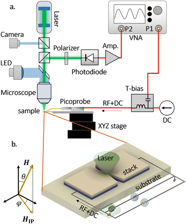
The experimental setup (Fig. 1a) employs a two-port vector network analyzer (VNA) to continuously excite the sample with an RF traveling wave (f0) and analyze its optical response. The SHNO is exposed to an external magnetic field H with variable in-plane (ϕ) and out-of-plane (θ) angles (see Fig. 1b). The RF signal from the VNA port 1 is combined with a direct current (IDC) through a bias-T and fed into the sample via a GSG picoprobe from GGB Industries. A continuous-wave 532 nm single-mode laser, focused to an approximate 380 nm diameter spot by a microscope objective with a numerical aperture of 0.75, is employed for probing. Both the laser power (Plaser) and the VNA RF power (PRF) can be continuously adjusted within the ranges 0 to 6 mW and −90 to 0 dBm, respectively. The sample holder is positioned under the microscope and controlled by an XYZ nanometric stage. The backscattered light from the SHNO passes through an analyzer set at a 45-degree angle relative to the polarization of the probe beam, resulting in an amplitude-modulated beam at the operational frequency of the SHNO. This modulated signal is then converted into an electrical voltage by a fiber-coupled broadband photoreceiver, amplified by 50 dB, and fed to the VNA port 2. For electrical measurements of the free-running SHNO, the signal collected by the coplanar waveguide and the picoprobe is measured using a spectrum analyzer; additional details can be found in ref. 17. All experiments were carried out under room conditions.
The VNA measures the scattering parameter S21 = V2/V1, where V1 is the excitation from port 1 and V2 the output of the photoreceiver after amplification at port 2. The VNA has an intermediate filter (IF) of 10 Hz, sufficient to visualize the autooscillation from a single SHNO structure. All measurements were performed in a single sweep without averaging, taking approximately 102 ms per data point. To achieve nanometric alignment, we actively stabilized the position of the SHNO using a homemade autofocus system and image recognition software from ThaTEC Innovation.
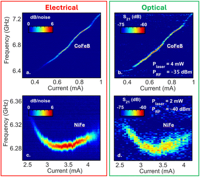
Fig. 2a and b compare the power spectral density (PSD) of a 300 nm wide CoFeB single nanoconstriction obtained through conventional electrical detection (dB over noise) and the optical measurement (in dB) using the VNA S21. The SHNO was subject to a H = 3600 Oe magnetic field at angles of θ = 65° and ϕ = 22.5°. For the optical measurement, the laser power was set to Plaser = 4 mW, and the RF power to PRF = −35 dBm. Consistent with the typical characteristics of CoFeB SHNOs, a low threshold current of approximately 0.45 mA is extracted together with a positive linear current dependence of the frequency, indicating the excitation of propagating spin waves above the ferromagnetic resonance (FMR) frequency, promoted by the perpendicular magnetic anisotropy.38
The corresponding electrical and optical measurements for a 300 nm wide NiFe SHNO, subject to a magnetic field of H = 6300 Oe, θ = 82°, and ϕ = 22.5°, and with Plaser = 2 mW and PRF = −40 dBm, are presented in Fig. 2c and d. The slight frequency offset observed in these measurements is attributed to minor deviations in the magnetic field settings during magnet resets. Typical for NiFe SHNOs,12 the device exhibits a significantly higher threshold current of about 2.5 mA and a nonmonotonic frequency shift that transitions from negative to positive with increasing electrical current. This behavior is characteristic of SHNOs made of materials with in-plane magnetic anisotropy when subject to oblique fields.39 In both samples, the optical measurements closely match the features observed with electrical detection. This congruence highlights the reliability and consistency of our optical measurements, demonstrating a strong correspondence with the electrical data.
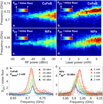
Electrical PSD measurements are routinely fit with Lorentzian distributions to extract the intrinsic linewidth and total power of the SHNO microwave signal. However, FR-MOKE does not strictly measure the intrinsic SHNO signal since it requires the SHNO to be injection-locked to an external reference RF signal. To investigate whether the optical data can still be used for such extraction, we measured the optical spectrum vs. both PRF and Plaser (Fig. 3) in the hope of extrapolating the measured response to the free-running and unperturbed PRF = Plaser = 0.
In the subsequent analysis, the spectrum is presented as the linear magnitude S21 normalized to the average value of the noise floor. Starting with the dependence on PRF (Fig. 3a and c), both the CoFeB and the NiFe SHNOs show the expected simple Arnold tongue behavior for injection locking: the first sign of locking appears at about PRF = −50 dBm, the central frequency of the SHNOs is essentially independent of PRF, and the locking bandwidth increases with PRF. Fig. 3e shows spectra from the CoFeB SHNO, taken at four values of PRF, together with Lorentzian fits from which we extract the peak height (S0) and the FWHM width (ΔVNA). The central frequency is essentially independent of the injected power. Fig. 3b and d show the corresponding PSD of the CoFeB and NiFe SHNOs as a function of Plaser. We detect the first signal at about 1 mW of laser power. Fig. 3f shows example spectra from the NiFe SHNO, taken at four values of Plaser, together with Lorentzian fits from which we again extract S0 and ΔVNA. In addition to their monotonic increase with Plaser, the central frequency, too, now shows a clear linear increase with Plaser. This is a direct effect of the laser heating of the SHNO, which was previously used for optothermal control of the SHNO frequency and will not be discussed further.31
We will first analyze and discuss the dependence on the injected RF power. Fig. 4 plots S0 and ΔVNAvs. P1/2RF for the CoFeB SHNO at three different values of Plaser. Plotted against P1/2RF, ΔVNA shows a linear dependence for all SHNOs at all investigated laser powers, confirming the expected square root power dependence of the injection locking bandwidth. ΔVNA increases slightly with Plaser, which we will discuss in more detail below. In contrast, S0 shows a non-linear dependence on P1/2RF, initially being linear and then asymptotically saturating at a value that increases linearly with Plaser. This dependence arises from the VNA technique being solely sensitive to the coherent response, i.e. to magnons locked to the injection. Thus, at low injected power levels, both the locking range and the coherent fraction of the magnons are small, but as PRF increases, the coherent fraction grows. However, once the mode fully synchronizes with the RF source, all magnons within the mode oscillate coherently with the injected signal, resulting in the maximum detected amplitude, and any further increases in PRF yield no proportional gains in signal strength. Therefore, the dependence S0(PRF) represents the transformation of the PSD of the noisy oscillator in the vicinity of the injected frequency,40,41 which can be rewritten as:
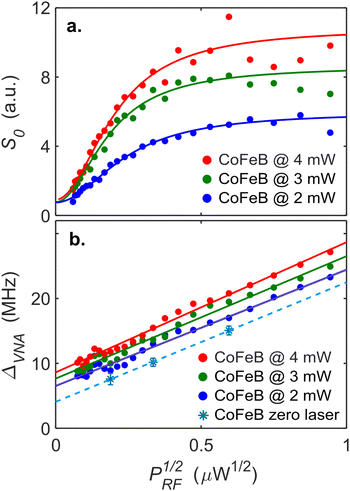 | ||
| Fig. 4 (a) The peak height (S0) and (b) linewidth (ΔVNA) vs. P1/2RF, as extracted from Lorentz fits to the normalized S21 from the CoFeB SHNO. Solid lines in a. represent fits to eqn (1). Solid lines in b. are linear fits w.r.t. P1/2RF. The pale blue star symbols denote the zero-laser-power intercepts from fits to the experimental data in Fig. 5b. The dashed blue line is a linear fit. When extrapolated to zero RF power, it yields the intrinsic linewidth (Δf = 4.1 MHz) of the free-running SHNO (see text). | ||
We now turn to the impact of Plaser. Fig. 5 plots S0 and ΔVNAvs. Plaser for the CoFeB SHNO at three different values of PRF. S0 is directly proportional to Plaser, simply reflecting the linear dependence of the photodiode (Fig. 5a). There is a slight deviation from the linear behavior towards higher Plaser, which we ascribe to heating from the laser. The deviation seems to start at lower Plaser for stronger injection, which may reflect the combined effect from both optical and electrical heating.
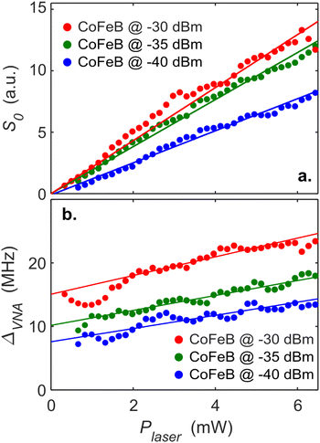 | ||
| Fig. 5 Extracted (a) S0 and (b) ΔVNAvs. Plaser for the CoFeB SHNO. Solid lines represent linear fits to the data. The intercepts with Plaser = 0 of the fits in b. are shown as pale blue stars in Fig. 4b and used to extract the intrinsic free-running SHNO linewidth (Δf). | ||
Since the detection is coherent with the injection signal, the measured ΔVNA shown in Fig. 5b is approximately the sum of the intrinsic SHNO auto-oscillation linewidth (Δf) and the phase-locking bandwidth (ΔPL) to the injected signal, ΔVNA ≃ Δf + ΔPL. Although the SHNO linewidth is substantially reduced by the injected signal over most of the locking range, it will approach that of the free-running SHNO at the band edges,40 and therefore add its full intrinsic value to ΔVNA. Both Δf and ΔPL are inversely dependent on the SHNO oscillation power ps:42
 | (1) |
From linear fits to the data in Fig. 5b, we can extract the linewidth broadening coefficient due to the laser as Claser = 1.2 ± 0.2 MHz mW−1. Extrapolation of these slopes to Plaser = 0 then yields ΔVNA at zero laser power for different values of PRF, which is the first step towards extracting the intrinsic SHNO linewidth. In a second step, we add these three extracted values for ΔVNA to the measured data in Fig. 4b and find that they follow the same square root dependence on PRF and with the same slope. A linear fit through these new data points yields broadening coefficients due to the injected RF power of CRF = 17.1 ± 2.2 MHz μW−1/2. Extrapolation to PRF = 0 finally provides us with estimates of the intrinsic SHNO linewidth of Δf = 4.1 ± 1.6 MHz, which is consistent with the electrically measured value of 5.9 MHz. Using this measurement and analysis protocol, it is, hence, possible to extract the intrinsic SHNO linewidth through optical measurements.
VNA-based detection excels in capturing the auto-oscillation phase, making it particularly advantageous for measuring the relative phase difference between individual SHNOs in SHNO arrays. In the next section, we will demonstrate its usefulness in reading out the individual phase states of two phase-binarized SHNOs of the type used in SHNO Ising machines.21 Phase binarization occurs when oscillators are injection-locked to an external signal at twice the oscillator frequency, so-called second harmonic injection locking (SHIL) or parametric pumping.43,44 The oscillators can then lock in two degenerate phase states, 0° 〈↑〉 and 180° 〈↓〉, with respect to a reference at the fundamental frequency f0. In our demonstration, we will use a pair of coupled SHNOs, which can have four potential states: 〈↑↑〉, 〈↓↓〉, 〈↑↓〉, and 〈↓↑〉.
Fig. 6 illustrates a modification of the original setup where the added electrical components are highlighted in blue text for easy identification, while the optical configuration remains the same. The RF frequency output from port 1 of the VNA is doubled by a multiplier and then passed through a high-pass filter, which suppresses the original frequency component f0 by 80 dB. The filtered signal is then routed through a circulator into the T-bias/picoprobe circuitry. The electrical signal reflected from the SHNO sample is guided back by the circulator to a spectrum analyzer, passing through a low-pass filter that attenuates the 2f0 component by 80 dB, before being amplified by a 70 dB low noise amplifier.
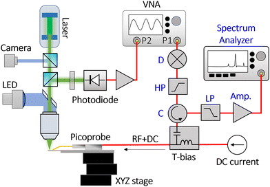 | ||
| Fig. 6 Schematic for parametric injection. (D) Frequency multiplier, (HP) high-pass filter, (C) circulator, (LP) low-pass filter. Other component labels are referenced as indicated in Fig. 1. | ||
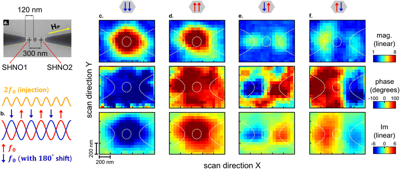
We conducted scanning imaging on a NiFe/Pt SHNO 2 × 1 array operating at a frequency of 8.25 GHz, a drive current of 3.75 mA, and a laser power of 2 mW. The sub-harmonic injection power was slowly varied between −10 and 0 dBm until the desired phase state was found and remained stable.21 The array comprises two oscillators with a constriction width of 120 nm and a center-to-center pitch of 300 nm (see Fig. 6a). The device was exposed to a magnetic field of 6200 Oe at field angles of θ = 82° and ϕ = 22.5°. The array exhibits robust synchronized states, characterized by well-defined phase-binarized values of 0° 〈↑〉 and 180° 〈↓〉 of each oscillator. While for an ideal SHNO array, the phase-binarized states would be pair-wise degenerate in their electrical signal and hence indistinguishable, real SHNOs possess intrinsic biases due to imperfections from the fabrication process, lifting this degeneracy and producing variations in output power for the four states.21 Although determining the 2-dimensional phase state of the device from its electrical output is not feasible a priori, a discrete change in the total auto-oscillation amplitude, monitored by the spectrum analyzer, denotes a state switch in the device. We exploit this characteristic and monitor the electrical microwave signal on the spectrum analyzer to ensure the stability of the system's phase state during the optical measurements.
Fig. 7 presents spatial maps of the magnitude, phase, and imaginary part of the S21 parameter for the four possible states of the SHNO system. The measurement area was 1 × 0.8 μm with a step resolution of 50 nm, and the VNA integration time per pixel was 102.3 ms, without averaging. The high acquisition speed enables completing the measurement within minutes, obviating the need for active stabilization of the sample position. The magnitude maps illustrate the mutual phase/antiphase synchronization of the SHNOs, emphasizing the high-power output of the phase-synchronized states. In these states, the individual phases of the two SHNOs are virtually identical, with only the smallest phase difference between them. While the spatial resolution is insufficient to observe the individual SHNOs in the magnitude of the signal, the phase sensitivity of the VNA clearly allows us to conclude that there are two distinct areas with slightly different phases.
In the antiphase synchronization states, the maps change completely. First, the intensity drops dramatically compared to the in-phase state. Second, the individual oscillators now also become clearly visible in the magnitude maps, as two distinct intensity areas can be observed. Both these dramatic differences are results of coherent destructive wave interference within this region. As the oscillator separation and the laser spot size are about the same, the destructive interference affects the entire map. However, the cancellation is only complete half-way between the oscillators, which leaves partial intensities at the oscillator locations. Further insights are gained by examining the phase phase information in the S21 signal, clearly revealing the relative anti-phase state of the two oscillators. In addition, the phase map shows a remarkable spatial resolution of about 100–150 nm, which is much below the diffraction limit. The phase maps extend well outside the auto-oscillating regions, where it is strictly speaking not well defined since the magnitude of S21 falls into the noise. It may therefore be more useful to look at the imaginary part of S21, which simultaneously show both the intensity and the phase state of the auto-oscillating regions. In this specific measurement, we calculated a contrast of approximately 31 dB between the average noise floor and the maximum of the imaginary component of S21.
Conclusions
We demonstrate a robust phase and frequency-resolved microscopy technique for characterizing the magnetic auto-oscillations of nano-constriction based spin Hall nano-oscillators. The detailed characterization of both single and interacting SHNOs made from two distinctly different material systems highlights the technique's robustness and its potential for wider applications. Our approach enables the measurement of key parameters of the SHNOs, including their frequency, amplitude, locking bandwidth to externally injected RF signal, and response to optothermal tuning. Notably, the technique allows for the effective de-embedding of perturbing effects from the injected power and the laser heating, providing optical estimates of the SHNO linewidth even in its free-running state. The technique offers significant advantages over alternative methods optical methods. For instance, our approach surpasses the frequency resolution limits of Brillouin light scattering measurements, which is typically constrained by the Tandem Fabry–Pérot interferometer's resolution of around 100 MHz. In contrast, our method benefits from the vector network analyzer's (VNA) orders of magnitude better resolution, typically below the kHz range. Moreover, unlike interferometry, cavity-based spectrometers that necessitate continuous scanning and stabilization of the reference wavelength, our technique facilitates continuous wave acquisition, significantly speeding up the acquisition process by orders of magnitude. Finally, a key feature of this technique is the very sensitive phase-resolved characterization of interacting SHNOs, crucial for using phase-binarized SHNOs in Ising machines, where the technique easily resolves the phase states of SHNOs separated by 300 nm, with a spatial resolution of 150 nm.Author contributions
A. Aleman: instrumentation design & construction (lead), experimental design (equal), development & design of methodology (lead), software development (lead), data acquisition (lead), data curation (equal), formal analysis (lead), original draft preparation (lead), writing – reviewing & editing (equal). A. A. Awad: conceptualization and original idea (lead), experimental design (equal), data curation (equal), research planning (equal), writing – reviewing & editing (equal). S. Muralidhar software development (supporting), investigation (supporting). R. Khymyn theoretical analysis (lead), critical review (supporting). A. Kumar sample preparation (equal), data acquisition (supporting). A. Houshang: sample preparation (equal). D. Hanstorp: project supervision (supporting), funding acquisition (supporting), critical review (supporting). J. Åkerman project supervision & management (lead), research planning (equal), data curation (equal), writing – review & editing (lead), funding acquisition (lead), critical review (lead).Data availability
Data for this work is available at Data Science Bank in the link: https://www.scidb.cn/en/s/rMZJn.Conflicts of interest
There are no conflicts to declare.Acknowledgements
This work was partially supported by the Horizon 2020 research and innovation programmes No. 835068 “TOPSPIN” and No. 899559 “SpinAge”, the Swedish Research Council (VR Grant No. 2016-05980), and the Knut and Alice Wallenberg Foundation.Notes and references
- T. Chen, R. K. Dumas, A. Eklund, P. K. Muduli, A. Houshang, A. A. Awad, P. Dürrenfeld, B. G. Malm, A. Rusu and J. Åkerman, Proc. IEEE, 2016, 104, 1919–1945 Search PubMed.
- J. Grollier, D. Querlioz, K. Y. Camsari, K. Everschor-Sitte, S. Fukami and M. D. Stiles, Nat. Electron., 2020, 3, 360–370 CrossRef PubMed.
- J. Torrejon, M. Riou, F. A. Araujo, S. Tsunegi, G. Khalsa, D. Querlioz, P. Bortolotti, V. Cros, K. Yakushiji, A. Fukushima, H. Kubota, S. Yuasa, M. D. Stiles and J. Grollier, Nature, 2017, 547, 428–431 CrossRef CAS PubMed.
- M. Zahedinejad, A. A. Awad, S. Muralidhar, R. Khymyn, H. Fulara, H. Mazraati, M. Dvornik and J. Åkerman, Nat. Nanotechnol., 2020, 15, 47–52 CrossRef CAS PubMed.
- M. Zahedinejad, H. Fulara, R. Khymyn, A. Houshang, M. Dvornik, S. Fukami, S. Kanai, H. Ohno and J. Åkerman, Nat. Mater., 2022, 21, 81–87 CrossRef CAS PubMed.
- P. Dürrenfeld, A. A. Awad, A. Houshang, R. K. Dumas and J. Åkerman, Nanoscale, 2017, 9, 1285–1291 RSC.
- M. Haidar, A. A. Awad, M. Dvornik, R. Khymyn, A. Houshang and J. Åkerman, Nat. Commun., 2019, 10, 2362 CrossRef PubMed.
- M. Zahedinejad, H. Mazraati, H. Fulara, J. Yue, S. Jiang, A. A. Awad and J. Åkerman, Appl. Phys. Lett., 2018, 112, 132404 CrossRef.
- M. Ranjbar, P. Dürrenfeld, M. Haidar, E. Iacocca, M. Balinskiy, T. Le, M. Fazlali, A. Houshang, A. Awad, R. Dumas and J. Åkerman, IEEE Magn. Lett., 2014, 5, 3000504 Search PubMed.
- H. Mazraati, S. Chung, A. Houshang, M. Dvornik, L. Piazza, F. Qejvanaj, S. Jiang, T. Q. Le, J. Weissenrieder and J. Åkerman, Appl. Phys. Lett., 2016, 109, 242402 CrossRef.
- H. Mazraati, M. Zahedinejad and J. Åkerman, Appl. Phys. Lett., 2018, 113, 092401 CrossRef.
- A. Awad, A. Houshang, M. Zahedinejad, R. Khymyn and J. Åkerman, Appl. Phys. Lett., 2020, 116, 232401 CrossRef CAS.
- K. Wagner, A. Smith, T. Hache, J.-R. Chen, L. Yang, E. Montoya, K. Schultheiss, J. Lindner, J. Fassbender, I. Krivorotov and H. Schultheiss, Sci. Rep., 2018, 8, 16040 CrossRef PubMed.
- M. Tortarolo, B. Lacoste, J. Hem, C. Dieudonné, M.-C. Cyrille, J. Katine, D. Mauri, A. Zeltser, L. Buda-Prejbeanu and U. Ebels, Sci. Rep., 2018, 8, 1728 CrossRef CAS PubMed.
- H. Singh, A. Bose, S. Bhuktare, A. Fukushima, K. Yakushiji, S. Yuasa, H. Kubota and A. A. Tulapurkar, Phys. Rev. Appl., 2018, 10, 024001 CrossRef CAS.
- A. A. Awad, P. Dürrenfeld, A. Houshang, M. Dvornik, E. Iacocca, R. K. Dumas and J. Åkerman, Nat. Phys., 2017, 13, 292–299 Search PubMed.
- A. Kumar, H. Fulara, R. Khymyn, A. Litvinenko, M. Zahedinejad, M. Rajabali, X. Zhao, N. Behera, A. Houshang, A. A. Awad and J. Åkerman, Nano Lett., 2023, 23, 6720–6726 CrossRef CAS PubMed.
- R. Lebrun, S. Tsunegi, P. Bortolotti, H. Kubota, A. Jenkins, M. Romera, K. Yakushiji, A. Fukushima, J. Grollier, S. Yuasa and V. Cros, Nat. Commun., 2017, 8, 15825 CrossRef CAS PubMed.
- S. Kaka, M. Pufall, W. Rippard, T. Silva, S. Russek and J. Katine, Nature, 2005, 437, 389–392 CrossRef CAS PubMed.
- D. I. Albertsson, M. Zahedinejad, A. Houshang, R. Khymyn, J. Åkerman and A. Rusu, Appl. Phys. Lett., 2021, 118, 112404 CrossRef.
- A. Houshang, M. Zahedinejad, S. Muralidhar, R. Khymyn, M. Rajabali, H. Fulara, A. A. Awad, J. Akerman, J. Checinski and M. Dvornik, Phys. Rev. Appl., 2022, 17, 014003 CrossRef CAS.
- S. Boixo, T. F. Rønnow, S. V. Isakov, Z. Wang, D. Wecker, D. A. Lidar, J. M. Martinis and M. Troyer, Nat. Phys., 2014, 10, 218–224 Search PubMed.
- R. Hamerly, T. Inagaki, P. L. McMahon, D. Venturelli, A. Marandi, T. Onodera, E. Ng, C. Langrock, K. Inaba, T. Honjo, K. Enbutsu, T. Umeki, R. Kasahara, S. Utsunomiya, S. Kako, K.-I. Kawarabayashi, R. L. Byer, M. M. Fejer, H. Mabuchi, D. Englund, E. Rieffel, H. Takesue and Y. Yamamoto, Sci. Adv., 2019, 5, eaau0823 Search PubMed.
- S. O. Demokritov and V. E. Demidov, IEEE Trans. Magn., 2008, 44, 6–12 CAS.
- T. Hache, T. Weinhold, K. Schultheiss, J. Stigloher, F. Vilsmeier, C. Back, S. S. Arekapudi, O. Hellwig, J. Fassbender and H. Schultheiss, Appl. Phys. Lett., 2019, 114, 102403 CrossRef.
- V. Demidov, S. Urazhdin, H. Ulrichs, V. Tiberkevich, A. Slavin, D. Baither, G. Schmitz and S. Demokritov, Nat. Mater., 2012, 11, 1028–1031 CrossRef CAS PubMed.
- A. Smith, K. Sobotkiewich, A. Khan, E. A. Montoya, L. Yang, Z. Duan, T. Schneider, K. Lenz, J. Lindner, K. An, X. Li and I. N. Krivorotov, Phys. Rev. B, 2020, 102, 054422 CrossRef CAS.
- T. Ogasawara, Phys. Rev. Appl., 2023, 20, 024010 CrossRef CAS.
- M. Buess, T. P. Knowles, R. Höllinger, T. Haug, U. Krey, D. Weiss, D. Pescia, M. R. Scheinfein and C. H. Back, Phys. Rev. B: Condens. Matter Mater. Phys., 2005, 71, 104415 CrossRef.
- T. M. Spicer, P. S. Keatley, M. Dvornik, T. H. Loughran, A. A. Awad, P. Dürrenfeld, A. Houshang, M. Ranjbar, J. Åkerman, V. V. Kruglyak and R. J. Hicken, Appl. Phys. Lett., 2018, 113, 192405 CrossRef.
- S. Muralidhar, A. Houshang, A. Alemán, R. Khymyn, A. A. Awad and J. Åkerman, Appl. Phys. Lett., 2022, 120, 262401 CrossRef CAS.
- T. Sebastian, K. Schultheiss, B. Obry, B. Hillebrands and H. Schultheiss, Front. Phys., 2015, 3, 139258 Search PubMed.
- M. L. Schneider, J. M. Shaw, A. B. Kos, T. Gerrits, T. J. Silva and R. D. McMichael, J. Appl. Phys., 2007, 102, 103909 CrossRef.
- J. M. Shaw, T. J. Silva, M. L. Schneider and R. D. McMichael, Phys. Rev. B: Condens. Matter Mater. Phys., 2009, 79, 184404 CrossRef.
- Y. Shiota, S. Funada, R. Hisatomi, T. Moriyama and T. Ono, Appl. Phys. Lett., 2020, 116, 192411 CrossRef CAS.
- L. Liensberger, L. Flacke, D. Rogerson, M. Althammer, R. Gross and M. Weiler, IEEE Magn. Lett., 2019, 10, 1–5 Search PubMed.
- A. Kumar, M. Rajabali, V. H. González, M. Zahedinejad, A. Houshang and J. Åkerman, Nanoscale, 2022, 14, 1432–1439 RSC.
- H. Fulara, M. Zahedinejad, R. Khymyn, A. A. Awad, S. Muralidhar, M. Dvornik and J. Åkerman, Sci. Adv., 2019, 5, eaax8467 CrossRef CAS PubMed.
- M. Dvornik, A. A. Awad and J. Åkerman, Phys. Rev. Appl., 2018, 9, 014017 CrossRef CAS.
- H.-C. Chang, X. Cao, M. J. Vaughan, U. K. Mishra and R. A. York, IEEE Trans. Microwave Theory Tech., 1997, 45, 2035–2042 CrossRef.
- K. Kurokawa, IEEE Trans. Microwave Theory Tech., 1968, 16, 234–240 CrossRef.
- V. S. Tiberkevich, R. S. Khymyn, H. X. Tang and A. N. Slavin, Sci. Rep., 2014, 4, 1–7 Search PubMed.
- E. R. J. Edwards, H. Ulrichs, V. E. Demidov, S. O. Demokritov and S. Urazhdin, Phys. Rev. B: Condens. Matter Mater. Phys., 2012, 86, 134420 CrossRef.
- L. Yang, A. A. Jara, Z. Duan, A. Smith, B. Youngblood, R. E. Arias and I. N. Krivorotov, Phys. Rev. B, 2022, 106, 144410 CrossRef CAS.
| This journal is © The Royal Society of Chemistry 2024 |

