Theoretical and experimental investigations of enhanced carbon nanotube-gold interface conductivity through nitrogen doping
Rui
Miao
a,
Yujian
Liang
a,
Ruolan
Wen
a,
Zhenhong
Jiang
a,
Yue
Wang
d and
Qingyi
Shao
 *bc
*bc
aSchool of Electronics and Information Engineering, South China Normal University, Foshan, 528225, China
bGuangdong Provincial Key Laboratory of Nuclear Science, Guangdong Provincial Key Laboratory of Quantum Engineering and Quantum Materials, Guangdong-Hong Kong Joint Laboratory of Quantum Matter, Guangdong Engineering Technology Research Center of Efficient Green Energy and Environment Protection Materials, School of Physics and Telecommunication Engineering, South China Normal University, Guangzhou 510006, China. E-mail: qyshao@163.com
cSchool of Science, Jiangnan University, Wuxi, Jiangsu 214122, China
dDepartment of Materials Science and Engineering, Yonsei University, Seoul 03722, Republic of Korea
First published on 21st November 2023
Abstract
It is necessary to establish high-quality contact between carbon nanotubes and metals in carbon-based devices. However, how to control and reduce contact resistance still remains unsolved. In this study, the effect of N doping in single-walled carbon nanotubes on the contact resistance with gold was studied by combining theoretical calculation with experimental methods. The theoretical results indicate that nitrogen doping in carbon nanotubes can control the bottom of the carbon nanotube conduction band downward, the Fermi level enters the conduction band, the height of the Schottky barrier between the bottom of the carbon nanotube conduction band and the gold Fermi level decreases, and the increase in doping concentration leads to the decrease of Schottky barrier width. As a result, the conductivity between the gold and carbon nanotube interface is enhanced. During experiments, the carrier density and the current of the gold and carbon nanotube device increase gradually with the increase in N doping concentration and a good electron transport channel is established between the gold and carbon nanotubes. The high-quality contact is crucial to reducing the size, improving the performance, and reducing the power consumption of carbon-based devices.
1. Introduction
Due to their enormous thermal conductivity, surface area, outstanding mechanical strength, and exceptionally high carrier mobility, single-walled carbon nanotubes (SWCNTs) have received a lot of interest.1–7 They are widely used in electronic devices, such as nanoelectronics, energy conversion/storage, sensors, catalysis, and flexible electronics, and are thought to be a good replacement for silicon-based materials due to its ultra-high carrier mobility in integrated circuits.8 Therefore, establishing high-quality conductive channels between carbon nanotubes and metal electrodes in electronic devices and integrated circuits is very important and challenging.9 The establishment of a high-quality conductive channel is of great significance for the preparation, size reduction, performance improvement, and power consumption reduction of carbon-based transistors. However, the work function difference and carrier density diversity between the two surfaces lead to the formation of an additional electric field between the metal and semiconductor. A Schottky barrier is also generated, which blocks the current.10Doping can effectively regulate the electrical properties of different devices.11–14 In order to circumvent the current blockage, the variation of contact resistance with the work function of the metal should be investigated. Based on the principle that metals and P-type semiconductors can generate ohmic contact when the work function of the metal is larger, Javey et al. modified a palladium electrode with hydrogen.15,16 According to a similar principle, Peng et al. studied the contact between scandium (Sc) and yttrium (Y) with relatively small metal work functions and carbon nanotubes. The Fermi level of Sc and Y matched with the bottom of the conduction band of the N-type SWCNTs to form an ohmic contact. According to the principle that electrons flow from an N-type semiconductor material with a large work function to a material with a small work function forming ohmic contacts, a method for preparing different electrodes on both sides of carbon nanotubes was proposed. Using this method, a single N-type SWCNTs field effect transistor (FET) was prepared using Pd metal with a large work function on one side and Sc or Y with a small work function on the other side.17–20
Besides, the contact resistance in devices can also be modified by changing dopants. In the successional study, Javey et al. doped potassium metal into carbon nanotubes to suppress the Schottky barrier in accomplished short-channel N-type SWCNTs FET and the contact resistance in source and drain electrodes.21 On this basis, a method of depositing excessive metal on the surface of SWCNTs is used to reduce the contact resistance. By means of high-temperature hydrogen reduction and electroless deposition, metal particles are deposited on the surface of SWCNTs, which improves the contact performance between the SWCNTs and metal, and the contact resistance decreases significantly.22,23 However, metals can cause material pollution, so organic solvents are implemented in the deposition process. In the early stage, Zhou et al. modulated doping along the length of semiconducting single-wall carbon nanotubes and doped poly methyl methacrylate (PMMA) on one side to form P-type and doped potassium (K) metal on the other side to form N-type. Electrostatic gating can tune the system into p–n junctions so it exhibits characteristics or negative differential conductance. At the same time, the influence of the band structure of both types of dopants was also investigated.24 Next, Biswas et al. utilized the SWCNTs network as a conductive channel to introduce oxygen adsorption and present P-type semiconductors. Benzyl viologen (BV) organic matter is chemically deposited on one side to convert a P-type semiconductor into an N-type semiconductor to form a PN junction.25 By doping triethyl oxonium hexachloroantimonate (OA) and polyethyleneimine (PEI), respectively, Zhang et al. obtained the steady P-type and N-type SWCNTs in air on both sides, and the central region remained in the original state.26 The results show that with the increase in doping, the forward current and rectification ratio of the diode increased, and the P-i-N junction diode with good performance is obtained. Previous researchers have done a lot of work to construct high-quality conductive channels between SWCNTs and metals; however, to better understand the mechanism, it is still necessary to further explore how to effectively control the Schottky barrier and enhance the conductivity between the metal electrodes and SWCNTs.
Therefore, this work not only reveals how to control the Schottky barrier to reduce the contact resistance by varying doping concentration in the SWCNTs, but also proves the results and method feasibility of the theoretical calculation by experiments. In the theoretical calculation, we took the smallest diameter self-supported (8,0) single-wall semiconductor carbon nanotubes as the research object to explore the effect of nitrogen-doped carbon nanotubes on the physical properties of materials and the contact resistance between metal electrodes. The theoretical results suggest that when N atoms are doped into SWCNTs, the Fermi level of SWCNTs moves up to the conduction band, and the bottom of the conduction band moves down. The position of the bottom of the SWCNTs conduction band and the Fermi level of the metal electrode together determine the height of the Schottky barrier. The concentration of dopants determines the width of the Schottky barrier. The calculation of the gold and single-walled carbon nanotube (Au-SWCNTs) contact model displays that the Schottky barrier can be effectively controlled and inhibited by doping N atoms in carbon nanotubes, and a high-quality conductive channel can be established between the carbon nanotubes and metal electrodes. Meanwhile, the experimental results also show that with the increase in nitrogen doping time, the carrier density increases and the contact resistance decreases. It provides a new method and theoretical basis for the preparation and development of carbon-based field effect transistors.
2. Method
This paper mainly consists of two parts: theoretical calculations and experiments. In the theoretical calculation part, the energy band structure, density of states (DOS), and work function of SWCNTs doped with different concentrations of N atoms are calculated. The influence of doping different concentrations of N atoms on the Schottky barrier between Au-SWCNTs is also discussed. Secondly, the contact model between Au-SWCNTs is constructed and the I–V curve and transmission spectrum of the model are calculated to explore the influence of the doping concentration on contact resistance. In the experimental part, SWCNTs and gold electrodes are assembled into prototype devices, and the SWCNTs are doped by local heating and vacuum vapor doping, and the I–V curve is tested to confirm the influence of the N element doping on the contact resistance of carbon nanotubes.2.1 Theory and computational details
Next, we use the non-equilibrium Green's function (NEGF) to investigate the influence of the N doping concentration on the contact resistance, the I–V curve, and the transmission spectrum of the Au-SWCNTs structure.
The calculation of electrical properties, current (I), is described by the Landauer–Büttiker formula:
 | (1) |
The recipe to determine the contact resistance is described in ref. 30 and 31 and we briefly reiterate it here. From the zero-bias calculations, we first calculate the transmission coefficient of the device, Tdev, using which the zero-bias conductance (Gdev) can be obtained as
 | (2) |
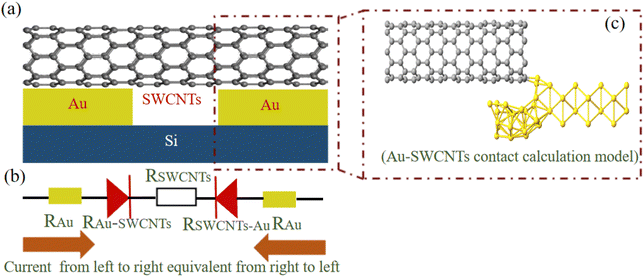
The corresponding resistance is simply Rdev = 1/Gdev. To calculate the contact resistance corresponding to the Au-SWCNTs interface, the intrinsic part of the resistance (RSWCNTs) corresponding to the semiconductor region needs to be subtracted. Thus, two separate calculations for the devices with and without the metal–semiconductor interface yield the contact resistance (RAu-SWCNTs = Rdev − RSWCNTs), respectively. In the above equations, e is the electronic charge, f is the Fermi function, h is the Planck's constant, Tdevice represents the transport coefficient of the system, and μL and μR refer to the chemical potentials of the left and right electrodes, respectively.
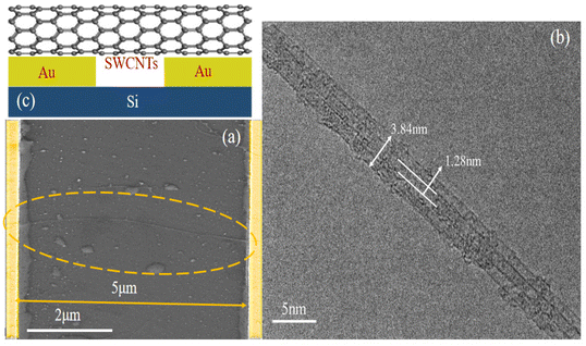
In the experiment, transmission electron microscopy (TEM JEM-1400 PLUS) is used to observe the morphology and diameter of carbon nanotubes in detail, as depicted in Fig. 2(b). The carbon nanotube bundle consists of three single-walled carbon nanotubes of the same diameter, with a diameter of 1.28 nm. In the experiment, the band gap width of carbon nanotubes was determined to be 0.57 eV by using the relationship between the band gap width and temperature. The Brillouin region and bandgap width of the carbon nanotubes are different due to the different chiral types. However, the width of the band gap determines the electrical properties of carbon nanotubes. Therefore, in order to narrow the gap between the experimental and theoretical calculations, (8,0) carbon nanotubes with a band gap close to the experimental width, a band gap of about 0.6 eV, were selected in the theoretical calculation. The (8,0) carbon nanotubes not only have a band gap close to that of the experimental carbon nanotubes but also have a mobility of nearly 200![[thin space (1/6-em)]](https://www.rsc.org/images/entities/char_2009.gif) 000 cm2 V−1 s−1 as the smallest diameter self-supported carbon nanotubes, which is very suitable for integrated circuits. Therefore, the contact between the gold (100) surface and unilateral (8,0) SWCNTs was simulated in theoretical calculations, as shown in Fig. 1(c).
000 cm2 V−1 s−1 as the smallest diameter self-supported carbon nanotubes, which is very suitable for integrated circuits. Therefore, the contact between the gold (100) surface and unilateral (8,0) SWCNTs was simulated in theoretical calculations, as shown in Fig. 1(c).
2.2 Experimental flow
In the experiment, SWCNTs (concentration ≥95%, OD: 1–2 nm, length: 4–20 μm, 0.25 mg) were dispersed into N,N-dimethylformamide solution (99.5%), and 2.5 μg ml−1 solution was prepared. The prepared solution is transferred to the electrode surface with a pipette, and SWCNTs and metal electrodes are assembled into experimental electrodes by electrophoresis. The electrode substrate is silicon, the surface has a 300 nm silicon dioxide insulation layer, the metal electrode is a 100 nm gold layer, and the channel spacing is 5 μm. The function generator (SPF40 digital synthesis function) is then connected to the two electrodes, and an alternating current with a voltage amplitude of 5 V and a frequency of 10 MHz is applied for electrophoretic assembly. After 1 minute of electrophoresis, the residual organic solution on the electrode surface was washed with nitrogen. Subsequently, the electrode assembly was completed by vacuum drying at 60 °C in the oven. The assembled electrode is shown in Fig. 2(a), as shown in the scanning electron microscope (SEM ZEISS Ultra 55) test diagram. The schematic diagram of carbon nanotubes in contact with the gold electrode is shown in Fig. 2(c). Next, 0.1 g of a melamine-doped source was weighed and placed in the vacuum device together with the prepared electrode. When the vacuum device starts pumping the gas and the pressure of the gas in the cavity reaches 30 Pa, the carbon nanotubes are preheated locally to make it easier to effectively dope locally. After preheating for five minutes, the melamine is rapidly heated to 1200 °C, and after heating for one minute, the melamine is completely vaporized, decomposed into the N element and incorporated into the carbon nanotubes.38–43 After maintaining the state for 5 minutes, stop the local heating device, gradually introduce air into the vacuum chamber, and retrieve the sample after the indoor gas reaches equilibrium. The carbon nanotubes were doped in situ several times by the above method. The I–V curves of carbon nanotubes were measured by a semiconductor analyzer, and the influence of N doping on the contact impedance of carbon nanotubes was analyzed.3. Results and discussion
3.1. Influence of doping on single-walled carbon nanotubes
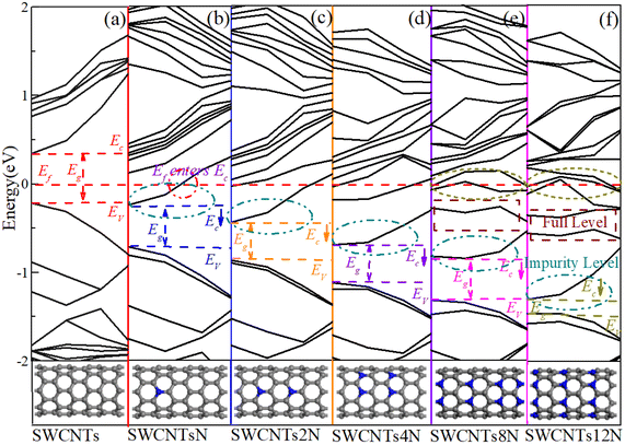
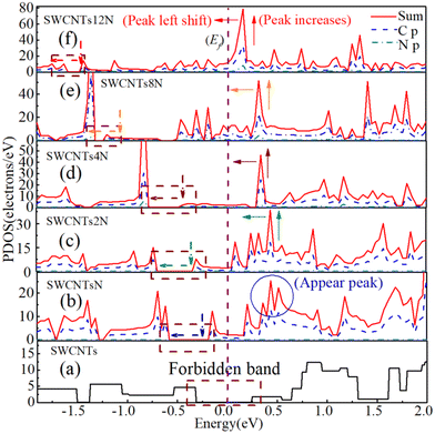
In this section, the effect of nitrogen doping on the energy band structure, DOS, and work function of (8,0) SWCNTs are investigated. We used the substitution method to dope N (1.04%), 2N (2.08%), 4N (4.16%), 8N (8.32%), and 12N (12.48%) atoms into (8,0) SWCNTs, respectively, as shown in Fig. 3. The energy band structure of the (8,0) SWCNTs at different doping concentrations was calculated, as shown in Fig. 3. The band structure in Fig. 3 is mainly divided into three states. The first state is the intrinsic semiconductor state of carbon nanotubes, as shown in Fig. 3(a). At this time, the band gap width of the carbon nanotubes is large, and the reason for the low number of charge carriers in carbon nanotubes is that only thermal excitation contributes. The energy band diagram of the contact between carbon nanotubes and metal electrodes is shown in Fig. 6(b). The height of the barrier depends on the position relationship between the Fermi level of the metal and the bottom of the conduction band of the carbon nanotubes. With the inclusion of N atoms, the band structure in the carbon nanotubes entered the light doping state Fig. 3(b and c), at which the bottom of the conduction band moved down, the band gap width decreased, and impurity levels appeared in the band. The impurity level crosses the Fermi level, indicating that N atom doping forms a local gap state.44,45 Electrons in the impurity band are more likely to transition to the conduction band, and the charge carriers produced in carbon nanotubes are mainly caused by the impurity band electron transition. The energy band diagram of the contact between carbon nanotubes and metal electrodes is shown in Fig. 6(d). Due to the appearance of impurity bands, the bottom of the conduction band moves down, height of the Schottky barrier begins to decrease, and the current in the device increases significantly. With the further incorporation of N atoms into the carbon nanotubes, the band structure enters the heavily doped state, as shown in Fig. 3(d–f). At this time, full bands appear below the Fermi level and the conduction bands across the Fermi level increase. The Fermi level enters the conduction band, which becomes an unfilled band, and carbon nanotubes are metallized. After heavy doping, the original semiconductor properties of the carbon nanotubes are transformed into metallic properties. The contact barrier height between the carbon nanotubes and metal electrodes remains basically unchanged, approximately determined by the Fermi level position rather than the usual position of the bottom of the conduction band. The contact between the carbon nanotubes and metal electrodes is mainly determined by the work function of heavily doped carbon nanotubes and the work function of metal electrodes.46 The contact barrier width between the carbon nanotubes and metal electrodes becomes very narrow as the doping concentration increases so that free electrons can tunnel through. The current generated at this time is mainly due to the tunneling contribution of free electrons, followed by the contribution of carriers crossing potential barriers caused by thermal motion.The DOS is calculated to gain a deeper understanding of the change in the physical properties of the SWCNTs by N-doping, and the results are shown in Fig. 4. The results obtained from the DOS analysis are consistent with those displayed in the energy band diagram above. The forbidden band of SWCNTs corresponds to the energy range with zero DOS ordinate, which may be too large for electrons to transition from the valence band to the conduction band under the action of an electric field. The forbidden band of SWCNTs decreases and moves down with the addition of nitrogen atoms. The peak value in DOS increases with the increase of nitrogen atoms and moves towards the Fermi level. As a result, due to the increase of peaks near the Fermi level, SWCNTs tend to approach the metallic properties. Although peaks produced by lightly doped nitrogen atoms in carbon nanotubes are not obvious in Fig. 4(b–d), contribution peaks of nitrogen atoms significantly increase with further insertion of nitrogen atoms. In the projected density of states (PDOS) of C and N atoms, the overlapping peaks in the energy range indicate a bonding between the carbon and nitrogen atoms. The calculated results of state density and energy band are basically consistent with the energy band structure in the ref. 35. Calculated results show that doping is an effective method for controlling the energy band structure of carbon nanotubes.47
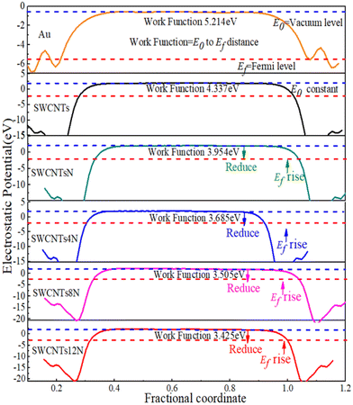
According to ref. 48, the Schottky barrier is due to the difference in work functions of two materials. Therefore, we calculated the work function of gold and SWCNT with different doping concentrations, as demonstrated in Fig. 5. The blue dotted lines are the vacuum levels and the red dotted lines are the Fermi level. The work function values of gold and pure carbon nanotubes are consistent with those in the experiment.48 The work function decreases with the increase in nitrogen atom doping concentration. The vacuum levels are in roughly the same position. The Fermi level moves upward with increasing doping concentration. The work function can be defined as the magnitude from the vacuum level to the Fermi level. The change in the Fermi level determines the change in the work function, which corresponds to the result that the Fermi level energy value decreases gradually with the increase in doping concentration.49
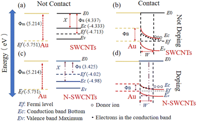
In Fig. 6, the energy band and work function of pure SWCNTs and SWCNTs doped with twelve nitrogen atoms were selected to draw the energy band structure diagram, and the influence of the change in the energy band on the Schottky barrier after doping was explored. The work function of the Au electrode (Φm) exceeds that of the SWCNTs (Φs), and the electrons pass from the semiconductor into the metal to equalize the Fermi levels, leaving behind a depletion region in the semiconductor in which the bands are bent upwards (process shown in Fig. 6(a) and (b)). The detailed description is as described in ref. 50 and will not be repeated in this paper. The barrier height can be described by the following formula.
| ΦB = Φm − X | (3) |
When the N atom is doped into SWCNTs, the Fermi level rises and the conduction band bottom falls, as shown in Fig. 6(c). The carbon nanotubes are in contact with the Au electrode, as shown in Fig. 6(d). After contact between Au and doped SWCNTs is established, the height of the Schottky barrier is determined by the Au work function and the doped SWCNTs electron affinity energy, as shown in eqn (3). The electron affinity energy in SWCNTs is determined by the bottom of the conduction band. With the increase in doping concentration, the conduction band moves down, and the electron affinity increases. The Au work function is determined by the Fermi level, and the Au work function remains unchanged, so the height of the Schottky barrier between Au and SWCNTs decreases. The height of the Schottky barrier is determined by the Au Fermi level and the bottom of the SWCNTs conduction band.
The width of the Schottky barrier can be described by the following formula.
 | (4) |
Here, εs is the dielectric constant of the semiconductor, Vbi is the built-in potential difference, VR is the added bias voltage value, and Nd is the doping concentration. With the increase of N atom doping concentration in SWCNTs, the Schottky barrier becomes thinner according to eqn (4).
3.2 Influence of doping on contact resistance
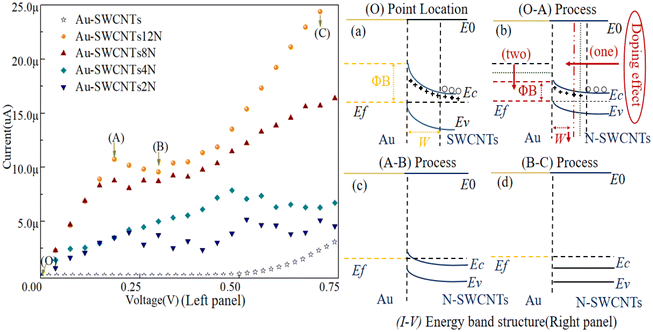
Next, we calculated the I–V curve, contact resistance, and transmission spectrum of the structure in Fig. 1(c) according to eqn (1) and (2). The electron transport properties of the contact model of Au-SWCNTs were investigated. The detailed I–V curves of the Au-SWCNTs contact model are shown in the inset of Fig. 7. In the illustration, there is no current in the range of ±0.5 V, mainly due to the high resistance of the SWCNTs. At the same time, the current direction (from SWCNTs to Au) is opposite to the direction of electron flow (from Au to SWCNTs), which indicates that the current under negative bias is about 4 times larger than the current under positive bias. The outcome clearly shows the appearance of the Schottky barrier. The calculated I–V characteristics corresponding to SWCNTs2N, SWCNTs4N, SWCNTs8N, and SWCNTs12N at different concentrations of N atoms are shown in Fig. 7. In the voltage interval from −1 V to 0 V, the current passing through the Au-SWCNTs structure gradually increases with increasing doping concentration. The reason for the increase is mainly due to the doping of N atoms, which provides more free electrons. In order to better understand the influence of doping on the electron transport performance of the Au-SWCNTs structure, we analyze the I–V curves at three different voltage intervals. In the voltage range from 0 V to 0.75 V, the relationship between current change and energy band structure change is shown in Fig. 8. In the figure, the left panel is the I–V curve, and the right panel corresponds to different stages of the energy band structure. The Au-SWCNTs contact interface is formed when SWCNTs contact the metal, and a Schottky barrier is formed on one side of SWCNTs, as shown in Fig. 8(a) on the right panel. When the applied voltage is 0, the current is 0, which corresponds to spot O in the left panel. With the increase in voltage, a current appears in the structure of Au-SWCNTs doped with N atoms. In this case, the current is mainly contributed by the electron tunneling effect. The increase in doping concentration leads to a decrease in the height of the Schottky barrier and a thinning of the thickness, making it easier for electrons to tunnel into the carbon nanotubes, thus increasing the current, corresponding to the O-A process in the left panel and the energy band structure shown in Fig. 8(b) on the right panel. On the other hand, Au-SWCNTs structures that are not doped with N atoms have few electrons passing through because of the Schottky barrier, so the current is close to zero. As the voltage continues to increase, the bottom of the conduction band in the carbon nanotubes continues to decrease. When it reaches the same level as the metal Fermi level, the tunneling current has the maximum value, corresponding to spot A in the left panel and the energy band structure shown in Fig. 8(c) on the right panel. As the forward voltage continues to increase, the overlap of the band starts to decrease until there is no overlap. The tunneling current has a minimum, corresponding to the A-B process in the left panel and the energy band structure shown in Fig. 8(d) on the right panel. When the forward voltage is further increased, the current is dominated by the drifting motion of electrons, which corresponds to the B-C process in the left panel. In the voltage range from 0.75 V to 1 V in Fig. 9, the negative differential resistance (NDR) effect is obvious under the SWCNTs12N doping concentration. The reason for the formation of the negative differential resistance (NDR) effect is based on the molecular orbital of the resonant charge transport channel being suppressed under an external bias.51 Therefore, with the increase in doping concentration, electrons gradually increase, and molecular orbitals are inhibited more obviously under the external bias pressure. It is also related to the use of carbon nanotubes for the electrode. Fig. 9 fitted the I–V curves at the voltage range from −1 V to 0.8 V. The slope of the fitted curve increases with the increase in doping concentration, and the current passing through the Au-SWCNTs interface increases gradually. At the same time, the slope change under negative voltage is smaller than that under positive voltage. It is concluded that the change of slope under negative voltage is caused by the change in SWCNTs resistance, and the change of slope under positive voltage is caused by the SWCNTs resistance and the Schottky barrier.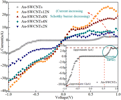 | ||
| Fig. 7 I–V curve results of the structural model (Fig. 1(c)) of the contact between the gold (100) plane and (8,0) SWCNTs. The inset section shows the I–V curves of undoped carbon nanotubes in contact with gold. The current passing through the Au-SWCNTs interface at plus or minus different voltages varies by a factor of four. The circled part of the figure shows no increase in current as the voltage increases, whereas this phenomenon does not occur when the voltage is reversed. It shows the appearance of the Schottky barrier. The whole figure shows the I–V curves of the contact between the carbon nanotubes doped with different concentrations of N atoms and gold. The current passing through the Au-SWCNTs interface increases with the increase in doping concentration. The curve with a slow current change at positive voltage becomes acute as the doping concentration increases. | ||
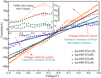 | ||
| Fig. 9 The fitting of I–V curves (Fig. 7) at a voltage from −1 V to 0.8 V. The slope of the fitted curve increases with the increase in doping concentration, and the current passing through the Au-SWCNTs interface increases gradually. At the same time, the slope change under negative voltage is smaller than that under positive voltage. It is concluded that the change of slope under a negative voltage is caused by the change in SWCNTs resistance. The change of slope under a positive voltage is caused by the SWCNTs resistance and contact resistance. In the inset, the I–V curves of voltages from 0.2 V–1 V show the appearance of a negative differential resistance effect, which increases with the increasing doping concentration. | ||
In order to thoroughly understand the influence of doping on resistivity, we combine molecular dynamics (MD) and the concept of electron transport in the framework of Landauer form to calculate the resistivity. The calculation method has already been described in the above method (section 2.1.1). The total device resistance is defined as a sum of the intrinsic SWCNTs and Au resistance plus a contact resistance Rc:
| RAu-SWCNT = Rc + RAu + RSWCNT | (5) |
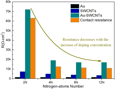
Eqn (5) thus defines the device resistance RAu-SWCNT, contact resistance Rc and gold resistance RAu, and carbon nanotube resistance RSWCNT. The calculation results are shown in Fig. 10. With the increasing doping concentration, the resistance of SWCNTs gradually decreases as the number of N atoms increases, which is consistent with the previous analysis of the properties of SWCNTs. The resistance of the device is mainly contributed by the contact resistance. As the doping concentration reaches a certain degree, the contact resistance and the device resistance reach a stable value. At the same time, the contact resistance and total resistance drop suddenly when doping with four atoms, so we consider that it is related to the Schottky barrier. When the doping concentration reaches a certain value, the bottom of the conduction band establishes an electron flow channel with the Fermi level of the metal. It is only the number of carriers that matters as the concentration increases.
In order to better understand the influence of doping on the electron transport of the model, the transmission spectrum at zero bias is calculated. The transmission energy curve represents the number of propagating channels for the conduction electrons with different energies. Fig. 11 shows that the transmission spectrum increases gradually with the increasing doping concentration at the zero Fermi level. Therefore, doping increases the transmission capacity of model electrons gradually. The peak near the red Fermi level increases with doping. The integral of the transmission area is the magnitude of the generated current. Therefore, it is consistent with the above results of the I–V curve.
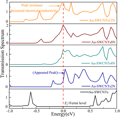 | ||
| Fig. 11 With the increase in N doping concentration, the peak value of the curve in the transmission spectrum near the Fermi level gradually increases, and the conductivity also increases. | ||
3.3 Experiments
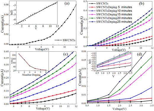
In this section, the influence of N doping concentration on the variation trend of contact resistance is verified again through experiments. In the experiment, we perform I–V curve tests on the electrodes assembled in Fig. 1(c). The results of the curve in Fig. 12(a) are nonlinear and consistent with the I–V curve of the semiconductor material, indicating that the semiconductor carbon nanotubes are connected to the metal electrode. In the inset, the fitting curves of ln(I) and V have a linear relationship, and it can be concluded that the Schottky barrier model is established, and the form is back-to-back.52,53 The back-to-back form is shown in Fig. 1(b) equivalent circuit, and the Au-SWCNTs-Au contact is similar to the Schottky diode back connection. Therefore, the actual contact between Au-SWCNTs in Fig. 2(a) was further proved. Fig. 12(b) shows the I–V curves of the SWCNTs doped with N atoms at different times. The results indicate that the current through the assembled electrode increases with the doping time. The I–V characteristics are modeled by treating the transport in the assembly electrode as in a metal–semiconductor–metal structure involving two Schottky barriers and a resistor in between these barriers, and the transport is shown to be dominated by the reverse-biased Schottky barrier under low bias (range) and by the semiconducting carbon nanotube at large bias (range). In contrast to the conventional Schottky diode, the reverse current in the Schottky barrier structure is not negligible, and the current is largely tunneling rather than thermionic.54 Therefore, the I–V curve in Fig. 12(b) is discussed in more depth. When the voltage is higher, the I–V curve is close to a straight line, and the resistance of the SWCNTs is the dominating term of the current at large bias voltage.55 In this large bias region, the I–V curve can be differentiated to obtain the resistance of the SWCNTs, as shown in eqn (6). | (6) |
R is the SWCNTs resistance, V is the I–V curve voltage, and I is the current. The change in resistance of SWCNTs from the intrinsic state to different doping times is measured under various voltages, as shown in the inset in Fig. 12(c). Other parameters are extracted from the 0.5–3.5 voltage section in the intermediate bias region where the reverse-biased Schottky barrier dominates the total current I.
 | (7) |
J is the current density through the Schottky barrier, S is the contact area associated with this barrier, E0 is a parameter that depends on the carrier density, and Js is a slowly varying function of applied bias. This logarithmic plot of the current I as a function of the bias V gives approximately a straight line (see Fig. 12(d) insert) of slope q/kT − 1/E0. With the increase in doping time, the carrier density (E0) increased from 26.24 mV to 26.95 mV. Electron concentration (n) can then be obtained via E0 and the electron mobility can be calculated using the relation μ = 1/nqρ, with ρ being the resistivity of the carbon nanotube. Therefore, we can conclude that the electron concentration increases gradually with the increase in doping time.56 As is mentioned in eqn (7) above, when the current through the Schottky barrier remains constant, the associated contact area can be reduced with the increase in the carrier density. At the same time, the device size changes with the contact area.
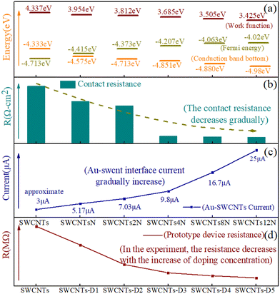
Theoretical calculation and experimental results are described above; Fig. 13 not only shows the influence of doping concentration on the work function, Fermi level, and bottom of the conduction band of carbon nanotubes but also exhibits the relationship between the three parameters on the interface current and contact resistance of Au-SWCNTs. At the same time, the variation in device resistance in the experiment is added and compared. In Fig. 13(a), with the increase in doping concentration, the three parameters aided a slow start, and the value of contact resistance basically reached stability. Similarly, the calculation results of the contact resistance are consistent with the changing trend of the three parameters. With the increase in doping concentration, the contact resistance of the Au-SWNCTs interface gradually decreases, as shown in Fig. 13(b). The decrease in the contact resistance leads to a gradual increase in the current passing through the Au-SWCNTs interface, as shown in Fig. 13(c). Therefore, the increase in doping concentration improves the electron transport performance of the Au-SWCNTs interface. The variation of device resistance in the experiment is shown in Fig. 13(d). Compared with the theoretical calculation results, it can be found that the variation trend of the device resistance is consistent with the variation trend of the contact resistance in the theoretical calculation. Thus, the influence of doping concentration on the interfacial contact resistance is demonstrated.
4. Conclusion
In summary, the effect of the N in situ doping in SWCNTs on the contact resistance with metal has been studied by combining theoretical calculations with experimental methods. The results of the theoretical calculation of the effect of N-atom doping on the physical properties of SWCNTs show that with the increase in doping concentration, the work function decreases, bottom of the conduction band moves down, width of the energy gap is reduced, and the Fermi energy level moves upward into the conduction band. The band structure analysis of Au-SWCNTs shows that the height of the Schottky barrier decreases with the conduction band bottom moving down, and the width of the Schottky barrier decreases with the increase in doping concentration. By calculating the Au-SWCNTs I–V curves, resistance, and transmission spectrum of the model, it can be seen that with N doping, the resistance formed by Au-SWCNTs in the model decreases and the current increases, indicating that doping N atoms can effectively reduce the resistance and contact resistance of SWCNTs. In the experiment, we tested the I–V curve of the self-assembled device. Through analysis, the Schottky barrier exists in the form of a back-to-back in the equivalent circuit of the device. With the increasing doping time, the carrier density gradually increases, and the contact resistance gradually decreases. Au-SWCNTs doping can not only improve the contact resistance but also reduce the contact area. This provides a solution for reducing the size, improving the performance, and reducing the power consumption of carbon-based devices.Author contributions
Qingyi Shao: conceptualization, methodology, formal analysis, data curation, resources, writing – original draft, writing – review and editing, supervision, project administration, funding acquisition. Rui Miao: investigation, experimental verification and theoretical calculation, formal analysis, data curation, writing – original draft. Yujian Liang: experimental verification. Ruolan Wen: theoretical calculation. Zhenhong Jiang: theoretical calculation. Yue Wang: writing – review and editing. All authors have read the paper, modified the final version, and agreed on the submission.Conflicts of interest
The authors declare that they have no known competing financial interests or personal relationships that could have appeared to influence the work reported in this paper.References
- F. S. Li, N. N. Wu, H. Kimura, Y. Wang, B. B. Xu, D. Wang, Y. F. Li, H. Algadi, Z. Guo, W. Du and C. X. Hou, Initiating Binary Metal Oxides Microcubes Electrsomagnetic Wave Absorber Toward Ultrabroad Absorption Bandwidth Through Interfacial and Defects Modulation, Nano-Micro Lett., 2023, 15(1), 220 CrossRef CAS.
- Y. P. Ma, C. X. Hou, H. Kimura, X. B. Xie, H. Y. Jiang, X. Q. Sun, X. Y. Yang, Y. P. Zhang and W. Du, Recent advances in the application of carbon-based electrode materials for high-performance zinc ion capacitors: a mini review, Adv. Compos. Hybrid Mater., 2023, 6, 2 CrossRef.
- Y. P. Ma, X. B. Xie, W. Y. Yang, Z. P. Yu, X. Q. Sun, Y. P. Zhang, X. Y. Yang, H. Kimura, C. X. Hou, Z. H. Guo and W. Du, Recent advances in transition metal oxides with different dimensions as electrodes for high-performance supercapacitors, Adv. Compos. Hybrid Mater., 2021, 4(4), 906–924 CrossRef CAS.
- C. C. Dang, Q. Mu, X. B. Xie, X. Q. Sun, X. Y. Yang, Y. P. Zhang, S. Maganti, M. N. Huang, Q. L. Jiang, I. Seok, W. Du and C. X. Hou, Recent progress in cathode catalyst for nonaqueous lithium oxygen batteries: a review, Adv. Compos. Hybrid Mater., 2022, 5(2), 606–626 CrossRef.
- Z. Sun, H. J. Qi, M. H. Chen, S. T. Guo, Z. H. Huang, S. Maganti, V. Murugadoss, M. Huang and Z. H. Guo, Progress in Cellulose/Carbon Nanotube Composite Flexible Electrodes for Supercapacitors, Eng. Sci., 2022, 18, 59–74 CAS.
- F. S. Li, Q. Y. Li, H. Kimuraa, X. B. Xie, X. Y. Zhang, N. N. Wu, X. Q. Sun, B. B. Xu, H. Algadi, R. A. Pashameahg, K. Abdullah, H. Alanazi, W. Du, Z. H. Guo and C. X. Hou, Morphology controllable urchin-shaped bimetallic nickel-cobalt oxide/carbon composites with enhanced electromagnetic wave absorption performance, J. Mater. Sci. Technol., 2023, 25–259 CrossRef.
- S. Tang, Carbon Nanotubes for Active Refrigeration and Cooling in Micro and Mesoscale Systems, Eng. Sci., 2022, 18, 263–270 CAS.
- T. Wang, J. Zhang and Q. Shao, Tiny nano-scale junction built on B/N doped single carbon nanotube, Nanotechnology, 2019, 30(7), 75203 CrossRef CAS PubMed.
- S. H. Ke, H. U. Baranger and W. T. Yang, Contact transparency of nanotube-molecule-nanotube junctions, Phys. Rev. Lett., 2007, 99(14), 146802 CrossRef PubMed.
- W. J. Albery, G. J. O'Shea and A. L. Smith, Interpretation and use of Mott–Schottky plots at the semiconductor/electrolyte interface, J. Chem. Soc., Faraday Trans., 1996, 92(20), 4083–4085 RSC.
- G. H. Fan, Z. Y. Wang, K. Sun, Y. Liu and R. H. Fan, Doped ceramics of indium oxides for negative permittivity materials in MHz-kHz frequency regions, J. Mater. Sci. Technol., 2021, 61, 125–131 CrossRef CAS.
- G. Y. Yuan, T. Wan, A. BaQais, Y. Mu, D. P. Cui, M. A. Amin, X. D. Li, B. B. Xu, X. H. Zhu, H. Algadi, H. D. Li, P. Wasnik, N. Lu, Z. H. Guo, H. G. Wei and B. W. Cheng, Boron and fluorine Co-doped laser-induced graphene towards high-performance micro-supercapacitors, Carbon, 2023, 212, 118101 CrossRef CAS.
- Q. Mu, R. L. Liu, H. Kimura, J. C. Li, H. Y. Jiang, X. Y. Zhang, Z. P. Yu, X. Q. Sun, H. Algadi, Z. H. Guo, W. Du and C. X. Hou, Supramolecular self-assembly synthesis of hemoglobin-like amorphous CoP@N, P-doped carbon composites enable ultralong stable cycling under high-current density for lithium-ion battery anodes, Adv. Compos. Hybrid Mater., 2023, 6, 23 CrossRef CAS.
- W. Y. Yang, D. N. Peng, H. Kimura, X. Y. Zhang, X. Q. Sun, R. A. Pashameah, M. Alzahrani, B. Wang, Z. H. Guo, W. Du and C. X. Hou, Honeycomb-like nitrogen-doped porous carbon decorated with Co3O4 nanoparticles for superior electrochemical performance pseudo-capacitive lithium storage and supercapacitors, Adv. Compos. Hybrid Mater., 2022, 314–3157 Search PubMed.
- A. Javey, J. Guo, Q. Wang, M. Lundstrom and H. J. Dai, Ballistic carbon nanotube field-effect transistors, Nature, 2003, 424(6949), 654–657 CrossRef CAS.
- J. E. Fischer, R. S. Lee, H. J. Kim, A. Thess and R. E. Smalley, Conductivity enhancement in single-walled carbon nanotube bundles doped with K and Br, Nature, 1997, 388(6639), 255–257 CrossRef.
- Z. Y. Zhang, X. L. Liang, S. Wang, K. Yao, Y. F. Hu, Y. Z. Zhu, Q. Chen, W. W. Zhou, Y. Li, Y. G. Yao and J. Zhang, Doping-free fabrication of carbon nanotube based ballistic CMOS devices and circuits, Nano Lett., 2007, 7(12), 3603–3607 CrossRef CAS.
- Z. Chen, J. Appenzeller, J. Knoch, Y. M. Lin and P. Avouris, The Role of Metal–Nanotube Contact in the Performance of Carbon Nanotube Field-Effect Transistors, Nano Lett., 2005, 5(7), 1497–1502 CrossRef CAS.
- L. Ding, S. Wang, Z. Zhang, Q. S. Zeng, Z. X. Wang, T. Pei, L. J. Yang, X. L. Liang, J. Shen, Q. Chen, R. L. Cui, Y. Li and L. M. Peng, Y-contacted high-performance n-type single-walled carbon nanotube field-effect transistors: scaling and comparison with Sc-contacted devices, Nano Lett., 2009, 9(12), 4209–4214 CrossRef CAS PubMed.
- C. G. Qiu, Z. Y. Zhang, M. M. Xiao, Y. J. Yang, D. L. Zhong and L. M. Peng, Scaling carbon nanotube complementary transistors to 5 nm gate lengths, Science, 2017, 355(6322), 271–276 CrossRef CAS.
- A. Javey, R. Tu, D. B. Farmer, J. Guo, R. G. Gordon and H. J. Dai, High performance n-type carbon nanotube field-effect transistors with chemically doped contacts, Nano Lett., 2005, 5(2), 345–348 CrossRef CAS PubMed.
- P. Yotprayoonsak, K. Hannula, T. Lahtinen, M. Ahlskog and A. Johansson, Liquid-phase alkali-doping of individual carbon nanotube field-effect transistors observed in real-time, Carbon, 2011, 49(15), 5283–5291 CrossRef CAS.
- N. Park, A. R Lee, H. S. Kim, J. J. Kim and J. O. Lee, Controllable modification of the conduction properties of carbon nanotube devices through deposition of a metal overlayer onto the sidewalls, Phys. E, 2012, 44(7–8), 1539–1542 CrossRef CAS.
- C. W. Zhou, J. Kong, E. Yenilmez and H. J. Dai, Modulated chemical doping of individual carbon nanotubes, Science, 2000, 290(5496), 1552–1555 CrossRef CAS PubMed.
- C. Biswas, S. Y. Lee, T. H. Ly, A. Ghosh, Q. N. Dang and Y. H. Lee, Chemically doped random network carbon nanotube p-n junction diode for rectifier, ACS Nano, 2011, 5(12), 9817–9823 CrossRef CAS PubMed.
- X. D. Liu, C. X. Chen, L. M. Wei, N. T. Hu, C. J. Song, C. H. Liao, R. He, X. S. Dong, Y Wang, Q. R. Liu and Y. F. Zhang, A p-i-n junction diode based on locally doped carbon nanotube network, Sci. Rep., 2016, 6(1), 23319 CrossRef CAS.
- J. J. Palacios, A. J. Perez-Jimenez, E. Louis, E. SanFabián and J. A. Vergés, First-principles phase-coherent transport in metallic nanotubes with realistic contacts, Phys. Rev. Lett., 2003, 90(10), 106801 CrossRef CAS PubMed.
- A. Nurbawono, A. H. Zhang, Y. Q. Cai, Y. H. Wu, Y. P. Feng and C. Zhang, Nanowelding of carbon nanotube-metal contacts: An effective way to control the Schottky barrier and performance of carbon nanotube based field effect transistors, J. Chem. Phys., 2012, 136, 174704 CrossRef PubMed.
- C. Shao, C. K. Rui, J. X. Liu, A. Q. Chen, K. G. Zhu and Q. Y. Shao, First-Principles Study on the Electronic Transport Properties of B/P, B/As, and B/Sb Co-doped Single-Walled Carbon Nanotubes, Ind. Eng. Chem. Res., 2020, 59(44), 19593–19599 CrossRef CAS.
- H. Dixit, C. Niu, M. Raymond, V. Kamineni, R. K. Pandey, A. Konar, J. Fronheiser, A. V. Carr, P. Oldiges and P. Adusumilli, First-Principles Investigations of TiGe/Ge Interface and Recipes to Reduce the Contact Resistance, IEEE Trans. Electron Devices, 2017, 64(9), 3775–3780 CAS.
- T. Markussen and K. Stokbro, Metal-InGaAs contact resistance calculations from first principles. IEEE, 2016, p. 373 Search PubMed.
- S. Cui, P. Scharff, C. Siegmund, L. Spiess, S. H. Romanus, J. Schawohl, K. Risch, D. Schneider and S. Klötzer, Preparation of multiwalled carbon nanotubes by DC arc discharge under a nitrogen atmosphere, Carbon, 2002, 1645–1687 Search PubMed.
- M. Keidar, Factors affecting synthesis of single wall carbon nanotubes in arc discharge, J. Phys. D: Appl. Phys., 2007, 40(8), 2388–2393 CrossRef CAS.
- Y. Ando, X. Zhao, S. Inoue, T. Suzuki and T. Kadoya, Mass production of high-quality single-wall carbon nanotubes by H2–N2 arc discharge, Diamond Relat. Mater., 2005, 14(3), 729–732 CrossRef CAS.
- W. Deng, X. Xu and W. A. Goddard, A Two-Stage Mechanism of Bimetallic Catalyzed Growth of Single-Walled Carbon Nanotubes, Nano Lett., 2004, 4(12), 2331–2335 CrossRef CAS.
- Y. Su, Z. Yang, H. Wei, E. S. W. Kong and Y. F. Zhang, Synthesis of single-walled carbon nanotubes with selective diameter distributions using DC arc discharge under CO mixed atmosphere, Appl. Surf. Sci., 2011, 257(7), 3123–3127 CrossRef CAS.
- Q. R. Wu, Z. H. Ji, L. T. Xin, D. Li, L. L. Zhang, C. Liu, T. Yang, Z. J. Wen, H. M. Wang, B. W. Xin, H. Xue, F. S. Chen, Z. W. Xu, H. Z. Cui and M. S. He, Iron silicide-catalyzed growth of single-walled carbon nanotubes with a narrow diameter distribution, Carbon, 2019, 149, 139–143 CrossRef CAS.
- R. Chegel, Tuning electronic properties of carbon nanotubes by Boron and Nitrogen doping, Phys. B, 2016, 499, 1–16 CrossRef CAS.
- A. Chen, Q. Y. Shao and Z. C. Lin, Effects of phosphorus-doping upon the electronic structures of single wall carbon nanotubes, Sci. China, Ser. G: Phys., Mech. Astron., 2016, 8(52), 1139–1145 Search PubMed.
- X. H. Yao, K. J. Li, J. Q. Ye and Q. Y. Shao, First principles study on B/N pairs co-doping zigzag single-walled carbon nanotubes, Chem. Phys. Lett., 2016, 653, 144–148 CrossRef CAS.
- X. J. Shao, D. T. Li, J. Q. Cai, H. J. Luo and C. K. Dong, First-principles study of structural and work function properties for nitrogen-doped single-walled carbon nanotubes, Appl. Surf. Sci., 2016, 368, 477–482 CrossRef CAS.
- L. N. Chen, F. P. OuYang, S. S. Ma, X. Z. Wu, J. Xiao and H. Xu, First-principles investigation on B/N co-doping of metallic carbon nanotubes, Phys. Lett. A, 2010, 4343–4348 CrossRef CAS.
- W. Liu, W. T. Zheng and Q. Jiang, First-principles study of the surface energy and work function of III-V semiconductor compounds, Phys. Rev. B: Condens. Matter Mater. Phys., 2007, 75(23), 235322 CrossRef.
- U. J. Kim, D. Y. Ko, J. P. Kil, J. W. Lee and W. Park, Effect of the metal work function on the electrical properties of carbon nanotube network transistors, J. Korean Phys. Soc., 2012, 60(10), 1680–1684 CrossRef CAS.
- E. H. Rhoderick, Metal-semiconductor contacts, IEE Proc., Part I: Solid-State Electron Devices, 1982, 129(1), 1–14 CAS.
- Z. Q. Fan and K. Q. Chen, Negative differential resistance and rectifying behaviors in phenalenyl molecular device with different contact geometries, Appl. Phys. Lett., 2010, 96, 053509 CrossRef.
- S. Agarwal, S. K. Manhas and S. Dasgupta, Metal Carbon Nanotube Schottky Barrier Diode with Detection of Polar Non-polar Gases, IEEE, 2016, pp. 361–366 Search PubMed.
- W. J. Albery, G. J. OShea and A. L. Smith, Interpretation and use of Mott-Schottky plots at the semiconductor/electrolyte interface, J. Chem. Soc., Faraday Trans., 1996, 92(20), 4083–4085 RSC.
- H. Xie, X. Li, Y. Wang, C. Wang, R. Wang and Y. Peng, Novel Mobility Evaluation of Organic Semiconductor Based on Current-Voltage Characteristics of Schottky Contact, J. Vac. Sci. Technol., 2010, 30(04), 347–350 CAS.
- C. Y. Nam, D. Tham and J. E. Fischer, Disorder Effectsin Focused-Ion-Beam-Deposited Pt Contacts on GaN Nanowires, Nano Lett., 2005, 5(10), 2029–2033 CrossRef CAS.
- Z. Y. Zhang, C. H. Jin, X. L. Liang, Q. Chen and L. M. Peng, Current-voltage characteristics and parameter retrieval of semiconducting nanowires, Appl. Phys. Lett., 2006, 89, 039901 CrossRef.
- C. Y. Nam, D. Tham and J. E. Fischer, Disorder effects in focused-ion-beam-deposited Pt contacts on GaN nanowires, Nano Lett., 2005, 5(10), 2029–2033 CrossRef CAS.
- M. Giulianini, E. R. Waclawik, J. M. Bell and N. Motta, Current-voltage characteristics of poly(3-hexylthiophene) diodes at room temperature, Appl. Phys. Lett., 2009, 94(8), 083302 CrossRef.
- Z. Wang, W. Y. Zang, Y. M. Shi, X. Y. Zhu, G. F. Rao, Y. Wang, J. W. Chu, C. H. Gong, X. Y. Gao and H. Sun, Extraction and Analysis of the Characteristic Parameters in Back–to–Back Connected Asymmetric Schottky Diode, Phys. Status Solidi A, 2020, 217(8), 1901018 CrossRef CAS.
- Z. Y. Zhang, C. H. Jin, X. L. Liang, Q. Chen and L. M. Peng, Current-voltage characteristics and parameter retrieval of semiconducting nanowires, Appl. Phys. Lett., 2006, 89(3), 073102 CrossRef.
- J. Appenzeller, J. Knoch, M. Radosavljevic and P. Avouris, Multimode transport in Schottky-barrier carbon-nanotube field-effect transistors, Phys. Rev. Lett., 2004, 92(22), 226802 CrossRef CAS.
| This journal is © The Royal Society of Chemistry 2024 |

