
Atomic insight into the effects of precursor clusters on monolayer WSe2†
Yanxue
Zhang
,
Yuan
Chang
,
Luneng
Zhao
,
Hongsheng
Liu
 * and
Junfeng
Gao
* and
Junfeng
Gao
Key laboratory of Materials Modification by Laser, Ion and Electron Beams (Dalian University of Technology), Ministry of Education, Dalian, 116024, China. E-mail: liuhongsheng@dlut.edu.cn
First published on 27th December 2023
Abstract
Two-dimensional (2D) transition metal dichalcogenides (TMDCs) have been attracting much attention due to their rich physical and chemical properties. At the end of the chemical vapor deposition growth of 2D TMDCs, the adsorption of excess precursor clusters onto the sample is unavoidable, which will have significant effects on the properties of TMDCs. This is a concern to the academic community. However, the structures of the supported precursor clusters and their effects on the properties of the prepared 2D TMDCs are still poorly understood. Herein, taking monolayer WSe2 as the prototype, we investigated the structure and electronic properties of SeN, WN (N = 1–8), and W8−NSeN (N = 1–7) clusters adsorbed on monolayer WSe2 to gain atomic insight into the precursor cluster adsorption. In contrast to W clusters that tightly bind to the WSe2 surface, Se clusters except for Se1 and Se2 are weakly adsorbed onto WSe2. The interaction between W8−NSeN (N = 1–7) clusters and the WSe2 monolayer decreases with the increase in the Se/W ratio and eventually becomes van der Waals interaction for W1Se7. According to the phase diagram, increasing the Se/W ratio by changing the experimental conditions will increase the ratio of SeN and W1Se7 clusters in the precursor, which can be removed by proper annealing after growth. W clusters induce lots of defect energy levels in the band gap region, while the adsorption of W1Se7 and SeN clusters (N = 3–6, 8) promotes the spatial separation of photo generated carriers at the interface, which is important for optoelectronic applications. Our results indicate that by controlling the Se/W ratio, the interaction between the precursor clusters and WSe2 as well as the electronic properties of the prepared WSe2 monolayer can be effectively tuned, which is significant for the high-quality growth and applications of WSe2.
 Hongsheng Liu | Hongsheng Liu obtained his PhD degree in condensed matter physics from the Dalian University of Technology in 2016. He is currently an associate professor in the Department of Physics at Dalian University of Technology. His research interests include structure and property tuning of nanomaterials and the applications of nanoclusters in nanomedicine. |
Introduction
Two-dimensional (2D) layered transition metal dichalcogenides (TMDCs) belong to a large family that exhibit rich properties.1–5 Compared to zero-gap graphenes, semiconducting TMDCs with proper bandgaps have attracted much attention.6–10 Moreover, the band gap of these TMDCs is tunable via the number of layers and strain.11–15 Monolayer WSe2, a member of TMDCs, exhibits a typical sandwich structure, Se–W–Se, where the W atomic layer is surrounded by two Se atomic layers and can be mechanically exfoliated from the bulk WSe2.16–18 When the layer thickness of WSe2 is reduced to monolayer, an indirect-to-direct band gap transition is observed.19,20 WSe2 has large exciton binding energies,21–23 large carrier mobility,24–26 and large absorption coefficients in the range of infrared to visible region,27–29 which are promising in the field of photonics, optoelectronics, and photodetectors. In addition, WSe2 has excellent catalytic performance.30–33Surface-supported clusters have been extensively studied, as the interaction between clusters and substrates plays an important role in the performance of catalysts and the growth of 2D materials.34–43 For example, Au cluster depositions on a TiO2 surface can effectively catalyze CO oxidation.34,35 TiC-supported Ni clusters could capture and activate methane at room temperature.38 Chen et al. studied 134 bare and compound clusters anchored on 2D N vacancy W2N3 (NV-W2N3) by high-throughput screening and proposed that VNiCu cluster-anchored NV-W2N3 shows the best performance for electrocatalytic nitrogen reduction reactions.42 Theoretical calculations show that the interaction between phosphorene nanoflakes and substrates around 0.35 eV per P atom is moderate to maintain the 2D feature of the phosphorene nanoflake.36 The cesium iodide cluster prefers to form on monolayer graphenes, while 2D CsI forms only on bilayer graphenes.39 In addition, a multilayer reduced graphene oxide (rGO)-supported Co4W18 cluster shows excellent catalytic performance for Li2S deposition and oxidation and better for Li–S batteries.40 Zhang et al. theoretically investigated the structure and electronic properties of Li2Sn cluster adsorption on various 2D materials and revealed that a suitable interaction between the Li2Sn cluster and anchor materials can enhance the performance of Li–S batteries.44 The post-synthesis strategies by incorporating excess Mo into MoTe2 and MoSe2 can modify the phase structure and electronic properties.45
The high-quality synthesis of WSe2 is a prerequisite for its application. Chemical vapor deposition is the most common method for synthesizing WSe2.46–48 The selenium/tungsten (Se/W) ratio plays an essential role in the growth of monolayer WSe2 and determines the type of precursor clusters. For example, Yue et al. proposed a high Se/W ratio, and an elevated substrate temperature is better for the growth of monolayer WSe2.49 Li et al. realized the precise control of hetero-epitaxy direction by manipulating the metal/chalcogenide ratio.50 The theoretical calculations showed that at a high Se/W ratio, W1Se3 clusters are the dominant species in the growth process, and the diffusion barrier of W1Se3 clusters of only 0.4 eV promotes the growth along the in-plane direction.50 In contrast, in a low Se/W ratio atmosphere, the components of W1Sex (x = 1–3) coexist, and W1Se1 clusters have a large diffusion barrier of about 1.2 eV, which can act as a nucleation site favorable for the growth along the out-of-plane direction.50
At the end of the chemical vapor deposition growth of 2D TMDCs, the adsorption of excess precursor clusters on the sample is unavoidable. As discussed above, these precursor clusters will have significant effects on the properties of TMDCs. However, the structures of the supported precursor clusters and their interaction with the 2D TMDCs as well as the effects on the properties of the prepared 2D TMDCs are still poorly understood.
In this work, we systematically investigated the structures of WSe2-supported possible precursor clusters including SeN, WN (N = 1–8) and W8−NSeN (N = 1–7) as well as their influence on the electronic properties of WSe2 monolayer using first-principles calculations. The interaction between precursor clusters and the WSe2 monolayer strongly depends on the Se/W ratio. By tuning the Se/W ratio, WSe2 with weakly adsorbed precursor clusters can be obtained, and the precursor clusters are expected to be removed by proper annealing. Interestingly, weakly adsorbed precursor clusters (W1Se7 and SeN clusters (N = 3–6, 8)) will promote the spatial separation of photo generated carriers at the interface, which is important for optoelectronic applications. W clusters will tightly bind to the WSe2 surface and induce lots of defect energy levels in the band gap region. Our results provide an atomic insight into the precursor cluster adsorption on the WSe2 monolayer, which is significant for the high-quality growth and applications of WSe2.
Computational methods
Following previous works, the ground-state structure of bare WN or SeN (N = 1–8) clusters in vacuum was constructed manually. The possible structure of W8−NSeN (N = 1–7) clusters was searched using a self-developed comprehensive genetic algorithm (CGA) code implemented in the DMol3 program,51,52 which has been proved to be a reliable and powerful tool for cluster structure search.52 The W8−NSeN (N = 1–7) clusters were optimized using the double numerical basis including d-polarization function (DND) and the Perdew, Burke and Ernzerhof (PBE) functional within the generalized gradient approximation (GGA).53 There are no symmetry constraints in the structure optimization. The number of maximum iterations of each search is set to 3000, and 16 members are retained in the population.Vienna Ab initio Simulation Package (VASP)54 can handle the problem of cluster adsorption on the surface well and give results that are in good agreement with the experiments. For example, by investigating the differences in the structure and stability of carbon clusters of adjacent sizes using DFT calculations with the VASP code, the branched C21-3C clusters were proposed to have special stability on the Ru/Rh surface, revealing the true structure of the experimentally observed dominant clusters.55,56 By investigating boron clusters on the Cu(111) surface using DFT calculations with the VASP, Liu and co-workers predicted the growth mechanism of borophene on a metal surface,57 which was confirmed by later experiments.58,59 Recently, combining experiments and VASP theoretical calculations, Zhou and co-workers investigated the growth mechanism of 67 types of transition metal chalcogenides (TMCs) and transition metal phosphorous chalcogenides (TMPCs) on a silicon substrate.60 The calculations regarding the chemical transition between different phases of TMCs well matched the experimental observation. Therefore, for the study of W8−NSeN (N = 0–8) clusters on the WS2 monolayer layer, we adopted the VASP code.
The searched W8−NSeN (N = 1–7) cluster structure is then further optimized using the VASP code. The structure and electronic properties of the bare WN or SeN (N = 1–8) cluster and the composite W8−NSeN (N = 1–7) cluster adsorption on the monolayer WSe2 were studied by spin-polarized density functional theory (DFT) calculations implemented in the VASP. The GGA-PBE was used to tackle the exchange and correlation functional. The electron-ion interactions were described by the projector augmented wave (PAW) potentials.61 The Grimme scheme DFT-D3 with a Becke–Jonson damping approach was used to describe the van der Waals (vdW) interactions between the cluster and the substrate.62,63 A vacuum space larger than 20 Å along the z-direction was set to avoid the interactions between the periodic replicas. The energy cutoff of the plane wave basis set was 500 eV. The Monkhorst–Pack k-point mesh with a separation of 0.02 Å−1 was used to sample the Brillouin zones.64 All atoms were relaxed and the lattice was fixed. The total energy convergence criterion was 10−5 eV and the force convergence criterion was 0.01 eV Å−1. The diffusion barrier of a single W or Se atom on the monolayer WSe2 surface was simulated by the climbing-image nudged elastic band (CI-NEB) method.65,66 Four images were used to simulate the diffusion path. The charge transfer between the cluster and the monolayer WSe2 surface was obtained by Bader charge analysis.67 The simulated scanning tunneling microscopic (STM) images were obtained using the Tersoff–Hamann approximation.68 The distance from the surface was kept constant, and the details are listed in Table S1.†
Results and discussion
Before investigating the structures of WSe2-supported WN, SeN (N = 1–8) and W8−NSeN (N = 1–7) clusters, the primitive cell of monolayer WSe2 is fully relaxed. The calculated equilibrium lattice constant of monolayer WSe2 is 3.316 Å, which is in good agreement with the previous theoretical results.69–72 We then transformed the primitive cell of WSe2 into the orthogonal unit cell and created a (5 × 3) supercell, as shown in Fig. S1.† The lattice constants of the (5 × 3) supercell of WSe2 are 16.58 Å and 17.229 Å along the x- and y-directions, respectively. Such a dimension of the supercell is expected to sufficiently avoid the interactions between periodic replicas.We first studied the adsorption of a single W atom on the perfect WSe2 surface. Here, we consider three adsorption sites, including the top of the W atom (TW), the top of the Se atom (TSe) and the hollow (H) site, as shown in Fig. S1.† By comparing the total energy of the three adsorption sites, the most stable adsorption site of the single W atom on the monolayer WSe2 surface was obtained, i.e. the W atom prefers to adsorb on the TW site of the monolayer WSe2 surface, as shown in Fig. S2a† and Fig. 1a. Our results agree well with the previous study that the W atom prefers the TW site of the WSe2 surface, which verifies the accuracy of our work.73 In addition, we considered the possible configurations that the W single atom was buried within the WSe2 layer, as shown in Fig. S2d and e.† The W atom buried within the WSe2 layer can significantly reduce the energy and the configuration of the W atom embedded at the TW site has the lowest energy, which is in agreement with the result reported by Zheng et al.74 This phenomenon is very interesting and additional energy must be needed to trigger this process. In this paper, we will not consider the burial of W atoms, leaving the discussion of the formation mechanism in our next work.
 | ||
| Fig. 1 Top and side views of (a) WN (N = 1–8) and (b) SeN (N = 1–8) cluster adsorption on the monolayer WSe2 surface. The blue and orange spheres indicate W and Se atoms, respectively. For the sake of clarity, the substrate is shown as a stick. The adsorption energy of (c) WN (N = 1–8) and (d) SeN (N = 1–8) clusters on the substrate (yellow line) and the minimum atomic distance between clusters and the substrate (green line). | ||
We then investigated the possible adsorption configuration of WN (N = 2–8) clusters on monolayer WSe2. For each size, several different structures are constructed to find out the most stable one, as shown in Fig. S3–S9 in the ESI.† After geometry optimization, the most stable structures for WN (N = 1–8) are shown in Fig. 1a. For the W2 cluster on the WSe2 monolayer, the most stable configuration is that one W atom is set on the TSe site of the WSe2 surface and the other W atom is set on the hollow site and binds with two Se atoms. For the W3 cluster, after structure optimization, the linear W3 cluster is reconstructed into the triangle W3 cluster, which is the most stable configuration of W3 cluster adsorption on the monolayer WSe2 surface. Two W atoms of the W3 cluster bind with Se atoms on the surface with one W atom at the TW site and the other W atom at the TSe site. For W4 on WSe2, the most stable configuration is a tetrahedral W4 cluster with two W atoms at the TW site binding with Se atoms on the surface. The result indicates that the linear configuration is not favorable for the W4 cluster on the WSe2 surface. Therefore, we ignore linear clusters for larger W clusters. The stable W5 cluster is a pentahedral with two W atoms chemically binding with Se atoms on the surface. The W6 cluster prefers a triangular antiprism structure with three W atoms binding with Se atoms. For W7 and W8 clusters on the surface, four W atoms bind with Se atoms on the surface.
The ground state structure of bare WN (N = 1–8) clusters in vacuum has been widely studied theoretically, which is also optimized in this work, as shown in Fig. S10.†75,76 The calculated bond length of the W2 cluster is 1.860 Å, which is in agreement with the previous study, 1.835 Å.76 The structure of the free-standing W3 cluster is equilateral triangle with a bond length of 2.235 Å. For the size larger than 3, all the structures of the free-standing W cluster show 3D geometries. For example, the W4 cluster is a tetrahedron, the W5 cluster is a distorted trigonal bipyramid, and the W7 cluster is a distorted pentagonal bipyramid. Compared with Fig. 1a and Fig. S10,† we can see that the WN (N = 4–8) cluster is preferred to form 3D configuration irrespective of whether in vacuum or on substrate, which indicates that the W atom on the substrate showed consistent behavior with that in vacuum. However, the most stable configuration is slightly different from that in vacuum. For example, for the W2 cluster, the bond length of the W–W bond is 1.940 Å, slightly longer than that in vacuum by about 0.08 Å. For the W3 cluster, the shape of the W3 cluster on the WSe2 surface is distorted from equilateral triangle to irregular triangle with bond lengths of 2.134 Å, 2.414 Å and 2.317 Å, respectively. The bond lengths of the W–W bond in the W4 cluster are stretched from 2.540 Å to 2.839 Å. The minimum atomic distance between the WN (N = 1–8) cluster and the substrate is also marked in Fig. 1a. The single W atom has the smallest relative minimum atomic distance, 1.58 Å. The W8 cluster has the largest relative minimum atomic distance, 2.30 Å. The relative minimum atomic distance between WN (N = 2–7) clusters and the substrate is in the range of 1.58 Å–2.30 Å. To evaluate the possibility of cluster formation on the WSe2 surface, the formation energy is defined as follows:
| Ef = (Etotal − Esub − N × EX)/N, |
The formation energy of WN clusters in vacuum and on substrate is plotted in Fig. S11.† As the size increases, the formation energy gradually decreases. For supported WN (N = 1–8) clusters, the formation energy has a similar trend as in vacuum, but always lower in energy, indicating that the WSe2 monolayer can stabilize WN (N = 1–8) clusters. Larger W clusters have lower formation energies than those of smaller W clusters. Therefore, we investigated the energy barrier of single W atom diffusion on the WSe2 surface to form large W clusters, as shown in Fig. S12.† The initial state (IS) is set as two W atoms adsorbed on the two separate TW sites. In addition, the final state (FS) is a W2 cluster. As shown in Fig. S12,† the W2 cluster adsorption configuration is more stable than the configuration of the two separate W atoms. The calculated energy barrier of W atom diffusion on the WSe2 surface is 0.62 eV, and the small atom diffusion barrier indicates that the W atom is easy to diffuse, which implies that via W atom diffusion into the WSe2 surface, growing large W cluster is more feasible. The corresponding transition state (TS) is shown in Fig. S12c,† where a W atom is moved from the TW site to the nearby TSe site.
We then calculated the adsorption energy of the WN clusters on the monolayer WSe2 surface. The adsorption energy is defined as follows:
| Eads = (Etotal − Esub − EXN)/N |
Furthermore, the projected band structures of monolayer WSe2 with WN (N = 1–8) clusters on the surface were calculated (Fig. S13†). Compared to the pristine WSe2 monolayer, WN clusters induce many impurity states in the gap region. The Fermi level is close to the CBM, indicating that W clusters transfer electrons to the WSe2 monolayer and make the monolayer n-doped. In addition, the W1, W5 and W8 clusters will induce spin polarization (as shown in Fig. S13a, e and h†).
Next, we begin to investigate the structure of SeN (N = 1–8) cluster adsorption on the WSe2 surface. For single Se atoms, we consider five configurations, as shown in Fig. S14a–e.† The most favorable adsorption site is the TSe site (Fig. 1b), which is consistent with the previous results.77 In contrast with the W atom, the configuration with the Se atom embedded in the WSe2 layer is very high in energy.
For SeN (N = 2–8) clusters on monolayer WSe2, several different structures are constructed for each size to find out the most stable one, as shown in Fig. S15–S21 in the ESI.† After geometry optimization, the most stable structures for SeN (N = 1–8) are shown in Fig. 1b. For the Se2 cluster on the WSe2 monolayer, the most stable configuration is a Se dimer with one Se atom chemically bonded with one Se atom on the surface. When N > 2, no chemical bond appears at the SeN cluster/WSe2 interface. For Se5, Se6, Se7 and Se8, five-, six-, seven- and eight-membered rings are the most stable configurations.
The Se vapor is predominantly SeN (N < 8) cluster, as indicated by the mass spectra.78 Subsequently, the structure of the free-standing Se3 to Se8 clusters was theoretically calculated.79,80 We reproduced the previously predicted structure of free-standing SeN (N = 3–8), as shown in Fig. S22.† The structure of free-standing Se3 and Se4 clusters is an open triangular structure and an open planar tetragonal structure, respectively. From Se5 to Se8 clusters, the structure is buckled pentagon, hexagon, heptagon and octagon ring, respectively. Compared with the structure of the Se2 cluster in vacuum, the bond length of the Se–Se bond in the Se2 cluster on the substrate is extended from 2.194 Å to 2.230 Å. For the Se3 cluster, which is not bonded to the WSe2 surface, the length of the Se–Se bond in the Se3 cluster changed from two equal bond lengths of 2.228 Å to two unequal bond lengths of 2.292 Å and 2.251 Å, respectively, and the bond angle changed from 116.658° to 112.481°. Similar to the Se3 cluster, the Se4 cluster is not bonded to the substrate. The Se–Se bond in the Se4 cluster can be divided into two types, namely, two equivalent short Se–Se bonds (2.187 Å) and one longer Se–Se bond (2.785 Å). After adsorption on the WSe2 surface, the bond length of the short bond increased to 2.191 Å, and the longer bond length decreased to 2.682 Å. For the Se5 cluster, the length of the Se–Se bond slightly increased from 2.300 Å to 2.302 Å, 2.390 Å to 2.400 Å, and 2.387 Å to 2.391 Å, respectively. For the Se6 cluster, the length of the Se–Se bond increased from 3.364 Å to 3.370 Å. For the Se7 and Se8 clusters, the length of the Se–Se bond changed by less than 0.005 Å. The single Se atom has the smallest minimum atomic distance, 2.12 Å. This is followed by the Se2 cluster, 2.58 Å. The Se4 cluster has the largest minimum atomic distance, 3.35 Å.
The formation energy of SeN (N = 1–8) clusters in vacuum is shown in Fig. S23.† It can be seen that as the cluster size increases, and the formation energy gradually decreases. The Se8 cluster has the lowest formation energy of 0.26 eV per atom. The formation energy of SeN (N = 1–8) clusters on the monolayer WSe2 surface has a similar trend with SeN (N = 1–8) clusters in vacuum, but it is always lower than that in vacuum, indicating that SeN (N = 1–8) clusters prefer to be deposited on the monolayer WSe2 surface. Based on the formation energy of SeN (N = 1–8) clusters on the WSe2 surface, we can conclude that large-sized clusters are easily formed on the WSe2 surface. Therefore, the barrier of Se atom diffusion on the WSe2 surface to form large clusters was investigated, as shown in Fig. S24.† The initial state is two Se atoms on separate TSe sites and the final state is set at the Se2 cluster adsorption on the WSe2 surface. On the WSe2 monolayer, the Se2 cluster is more stable than the two separate Se atoms and the energy barrier of Se atom diffusion is 1.02 eV. The high barrier indicates that it is difficult to form large Se clusters by the diffusion of single Se atoms on the surface and that the direct deposition of the vapor large Se clusters on the surface is practical.
The adsorption energy of SeN (N = 1–8) clusters on the WSe2 monolayer is shown in Fig. 1d, from which we can see that the single Se atom has the largest adsorption energy (−1.69 eV per atom). The adsorption energy of Se2 to Se8 clusters is in the range of −0.14 to −0.31 eV per atom. Compared to WN (N = 1–8) clusters, SeN (N = 1–8) clusters have weaker interaction with the substrate. The minimum atomic distance between the SeN (N = 1–8) cluster and the substrate increases with the increase in cluster size, and is always greater than that between the WN (N = 1–8) cluster and the substrate. Especially, the interaction between SeN (N = 3–8) clusters and the WSe2 monolayer is weak vdW interaction, indicating their ease of removal under proper annealing.
To check the effect of SeN (N = 1–8) cluster adsorption on the electronic properties of WSe2, the projected band structures are plotted (shown in Fig. S25†). In general, few defects are induced in the band gap region, which is in sharp contrast with the case of W clusters. According to the location of the highest occupied molecular orbital (HOMO) and lowest unoccupied molecular orbital (LUMO) orbits of the SeN clusters, SeN clusters (N = 3–6, 8) would promote the spatial separation of photo generated carriers at the interface. The high efficiency charge separation is a key factor affecting the photocatalytic performance of semiconductors.81–87 For example, charge separation greatly improves the efficiency of CO2 photo-reduction and hydrogen evolution reactions.81,87 Therefore, the SeN (N = 3–6, 8) cluster deposition on the WSe2 surface provided an atomic level strategy to promote charge separation, which is important for optoelectronic applications.
For convenient experimental observation of the clusters, the scanning tunneling microscopic (STM) images of WN and SeN (N = 1–8) clusters are simulated and shown in Fig. 2. In general, the adsorbed WN clusters appear as a big bright point in the STM image, and the larger the cluster, the larger the bright point. For SeN clusters, they also appear as bright points and the patterns in STM images are more recognizable. For example, the Se2 cluster shows as a bone-like pattern and the Se8 cluster appears as an eight-membered ring.
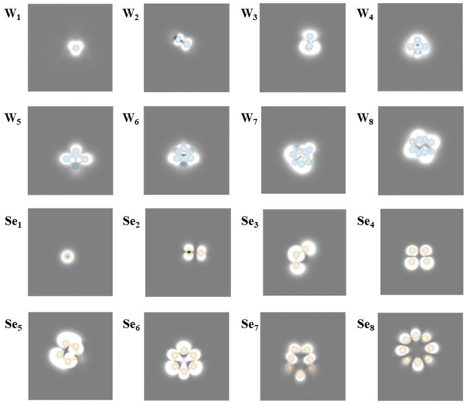 | ||
| Fig. 2 Simulated STM of WN (N = 1–8) and SeN (N = 1–8) cluster adsorption on the WSe2 surface at −0.6 V bias, respectively. | ||
To further illustrate the cluster-substrate interaction, the charge density difference and the corresponding Bader charge transfer between the clusters and the WSe2 monolayer are plotted, as shown in Fig. 3. The results show that WN (N = 1–8) clusters transfer electrons to the WSe2 monolayer, resulting in n-type doping of the monolayer WSe2. SeN (N = 1–4) clusters gain electrons from the WSe2 layer, while Se5 slightly transfers electrons to the WSe2 layer. For Se6, S7 and Se8 clusters, there is almost no electron transfer between clusters and the WSe2 layer. The less charge transfer between SeN clusters and the WSe2 layer again confirms the weak interaction at the interface which is in sharp contrast to WN clusters.
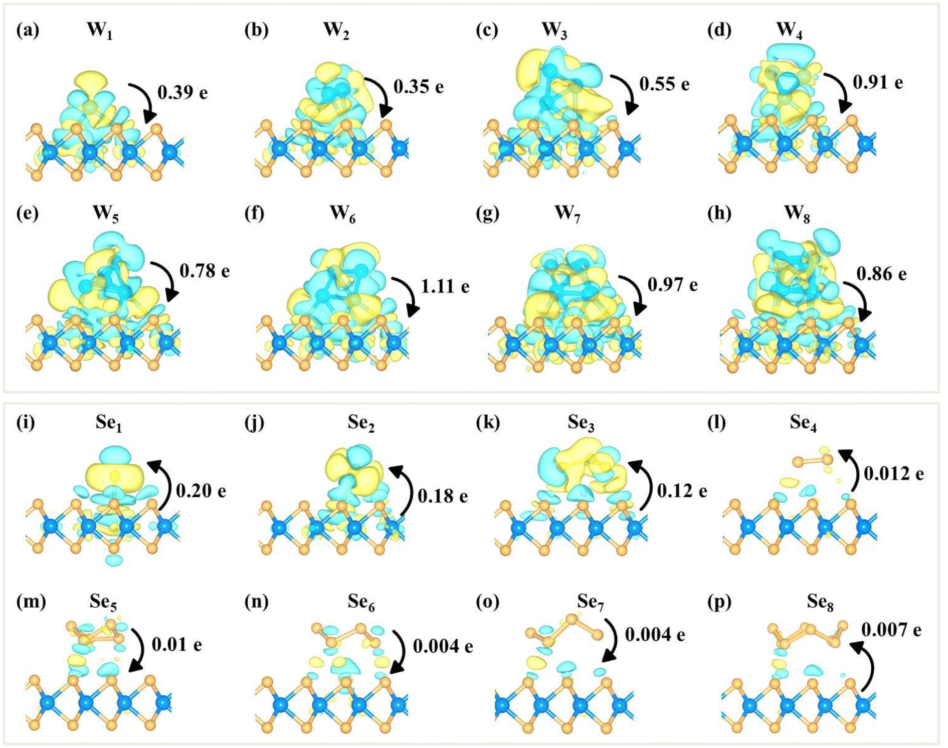 | ||
| Fig. 3 Charge density difference of (a–h) WN (N = 1–8) and (i–p) SeN (N = 1–8) clusters adsorbed on the WSe2 surface. The accumulation and depletion of charge density are represented in yellow and green colors. The value and direction of the Bader charge transfer are also marked. The isosurface value is 0.0005 e Bohr−3. | ||
In experiments, the selenium/tungsten (Se/W) ratio has a strong influence on the growing monolayer WSe2.50,88,89 Using the self-developed CGA software,52 several low-energy W8−NSeN (N = 1–7) binary clusters in vacuum were determined (shown in Fig. S26–S32†). The detailed discussion about the ground state (GS) structures of free-standing W8−NSeN (N = 1–7) binary clusters can be found in the ESI.† Subsequently, these searched W8−NSeN (N = 1–7) binary clusters were put on the WSe2 monolayer (shown in Fig. S33–S39†) to investigate supported W8−NSeN (N = 1–7) binary clusters. The most stable structures of the WSe2-supported W8−NSeN (N = 1–7) binary clusters are shown in Fig. 4a. In comparison, the WSe2 substrate has a great influence on the geometry of the compound clusters. For example, compared to the free-standing GS W7Se1 cluster, the supported GS W7Se1 cluster is distorted. The metastable W1Se7 cluster in vacuum (Fig. S32b†) becomes the most stable one when adsorbed on the surface (Fig. 4a). When the Se/W ratio is less than 7, the W8−NSeN (N = 1–6) clusters prefer to bond with the surface through W-Se chemical bonds. Therefore, W8−NSeN (N = 1–6) clusters interact strongly with the WSe2 surface. As the Se/W ratio increases, the number of chemical bonds at the interface decreases. When the Se/W ratio reaches 7, the minimum atomic distance between the cluster and the WSe2 substrate increases from 1.64 Å to 3.02 Å and no chemical bonds exist at the interface. The W1Se7 clusters prefer physical adsorption on the WSe2 surface. Therefore, by tuning the Se/W ratio, the interaction between W8−NSeN and the WSe2 layer can be effectively tuned.
 | ||
| Fig. 4 Top and side views of (a–g) W8−NSeN (N = 1–7) cluster adsorption on the monolayer WSe2 surface, the minimum atomic distance, charge density difference and corresponding Bader charge transfer. (h) Adsorption energy of W8−NSeN (N = 1–7) cluster adsorption on the monolayer WSe2 surface. (i) Minimum atomic distance of W8−NSeN (N = 1–7) cluster adsorption on the monolayer WSe2 surface. (j) Bader charge transfer of W8−NSeN (N = 1–7) cluster adsorption on the monolayer WSe2 surface. The negative value of the Bader charge transfer indicates that the cluster loses electrons and the positive value of the Bader charge transfer indicates that the cluster gains electrons. | ||
The charge density difference and the corresponding Bader charge transfer between the W8−NSeN (N = 1–7) cluster and the WSe2 surface are shown in Fig. 4 to reveal the interaction between the cluster and the substrate. When the number of Se atoms increases from 1 to 7, there is almost no electron transfer between the cluster and the substrate. The W1Se7 cluster transfers only 0.014 e to the substrate, again indicating the weak interaction between the W1Se7 clusters and the substrate. The W8−NSeN (N = 1–4) cluster donates electrons to the substrate, resulting in an n-type WSe2 monolayer, while the W8−NSeN (N = 5, 6) cluster accepts electrons from the substrate resulting in a p-type WSe2 monolayer. For W1Se7, there is almost no charge transfer.
For WN and SeN (N = 1–8) clusters, W8 and Se8 are the most stable on the WSe2 monolayer. To estimate the stability of binary W8−NSeN (N = 1–7) clusters, we constructed the phase diagram of W8, Se8 and W8−NSeN (N = 1–7) clusters on the substrate based on the chemical potential of W and Se atoms. The formation energy of W8−NSeN (N = 1–7) clusters as a function of W chemical potential (μW) and Se chemical potential (μSe) is defined as follows:
| Ef = Etotal − Esub − (8 − N) × μW − N × μSe, |
 | ||
| Fig. 5 Phase diagram of bare W8, Se8 and compound W8−NSeN (N = 1–8) clusters adsorbed on the WSe2 surface. | ||
The projected band structures of the WSe2 monolayer with W8−NSeN (N = 1–8) clusters on it are also examined, as shown in Fig. S41.† At a low Se/W ratio (N < 7), W8−NSeN clusters will induce many impurity states in the gap region like WN clusters. For the W1Se7 cluster, the LUMO and HOMO of the W1Se7 cluster are staggered with the valence band maximum (VBM) and conduction band minimum (CBM) of WSe2, implying that the W1Se7 cluster and WSe2 monolayer surface form a type-II band alignment, which will promote the spatial separation of photo generated carriers at the interface.
Briefly, among the WN, SeN (N = 1–8) and W8−NSeN (N = 1–7) clusters, SeN (N = 3–8) and W1Se7 clusters have low adsorption energy on the WSe2 surface, which are more easily removed from the surface to form clean monolayer WSe2. In addition, cluster adsorption on the WSe2 surface is an effective tool to modify the electronic properties of WSe2. The SeN (N = 3–6,8) and W1Se7 cluster adsorption could form a unique type-II band alignment. WN (N = 1–8) and W8−NSeN (N = 1–7) clusters induced a large number of impurity states in the band gap region of the pristine WSe2 monolayer. In this work, the dynamic process of cluster transition from W7Se1 to W1Se7 and the specific temperature needed to remove SeN clusters by annealing were not considered. The effect of the presence of hydrogen on the structure was also not considered. There are also interesting and important issues to be discussed and they are left to be solved in our next work.
Conclusions
In summary, the adsorption of possible precursor clusters WN and SeN (N = 1–8) as well as W8−NSeN (N = 1–7) on monolayer WSe2 was carefully investigated using first-principles calculations. The GS structures for these clusters in vacuum and on the WSe2 layer were well studied. The interaction between WN clusters and the WSe2 layer is very strong, so that it is hard to remove WN clusters. In contrast, the interaction between SeN clusters and the WSe2 layer is weak vdW interaction except for single Se atoms and Se dimers. The interaction between W8−NSeN and the WSe2 layer depends on the Se/W ratio. A high Se/W ratio (N = 7) results in weak interaction at the interface, while low Se/W (N < 7) results in W–Se chemical bonds at the interface. The stability of WN and SeN (N = 1–8) as well as W8−NSeN (N = 1–7) on monolayer WSe2 is related to the chemical potential of W and Se and the phase diagram is plotted. Increasing the Se/W ratio by changing the experimental conditions would increase the ratio of SeN and W1Se7 clusters in the precursor clusters, which can be removed by proper annealing. Moreover, WN clusters induce many defect states in the band gap region. SeN (N = 3–6, 8) and W1Se7 clusters will promote the spatial separation of photo generated carriers at the interface, due to the alignment of HOMO and LUMO of the clusters with the VBM and CBM of the WSe2 monolayer. This spatial separation is important for optoelectronic applications. Our results provide an atomic insight into the precursor clusters adsorbed on the WSe2 monolayer. We suggest that the interaction between the precursor clusters and the WSe2 monolayer as well as the electronic properties of the prepared WSe2 monolayer can be tuned by controlling the Se/W ratio, which is significant for the high-quality growth and applications of WSe2.Conflicts of interest
The authors declare no competing financial interest.Acknowledgements
This work is supported by the National Natural Science Foundation of China (12374253, 12374174, 12074053, 12004064, 91961204), the Fundamental Research Funds for the Central Universities (DUT22LK11, DUT22QN207) and the Research Fund for International Cooperation of DUT-BSU Joint Institute (ICR2202).References
- Q. H. Wang, K. Kalantar-Zadeh, A. Kis, J. N. Coleman and M. S. Strano, Nat. Nanotechnol., 2012, 7, 699–712 CrossRef CAS.
- S. Manzeli, D. Ovchinnikov, D. Pasquier, O. V. Yazyev and A. Kis, Nat. Rev. Mater., 2017, 2, 17033 CrossRef CAS.
- Z. Hu, Z. Wu, C. Han, J. He, Z. Ni and W. Chen, Chem. Soc. Rev., 2018, 47, 3100–3128 RSC.
- X. Wu, H. Zhang, J. Zhang and X. W. Lou, Adv. Mater., 2021, 33, 2008376 CrossRef CAS.
- T. Heine, Acc. Chem. Res., 2014, 48, 65–72 CrossRef.
- A. K. Geim, science, 2009, 324, 1530–1534 CrossRef CAS PubMed.
- C. H. Lui, L. Liu, K. F. Mak, G. W. Flynn and T. F. Heinz, Nature, 2009, 462, 339–341 CrossRef CAS.
- J. Kang, S. Tongay, J. Zhou, J. Li and J. Wu, Appl. Phys. Lett., 2013, 102, 012111 CrossRef.
- K. F. Mak, D. Xiao and J. Shan, Nat. Photonics, 2018, 12, 451–460 CrossRef CAS.
- K. F. Mak and J. Shan, Nat. Photonics, 2016, 10, 216–226 CrossRef CAS.
- C.-H. Chang, X. Fan, S.-H. Lin and J.-L. Kuo, Phys. Rev. B: Condens. Matter Mater. Phys., 2013, 88, 195420 CrossRef.
- R. Frisenda, M. Drüppel, R. Schmidt, S. Michaelis de Vasconcellos, D. Perez de Lara, R. Bratschitsch, M. Rohlfing and A. Castellanos-Gomez, npj 2D Mater. Appl., 2017, 1, 10 CrossRef.
- C. Hsu, R. Frisenda, R. Schmidt, A. Arora, S. M. Vasconcellos, R. Bratschitsch, H. S. J. Zant and A. Castellanos-Gomez, Adv. Opt. Mater., 2019, 7, 1900239 CrossRef.
- L. Mennel, M. Paur and T. Mueller, APL Photonics, 2019, 4, 034404 CrossRef CAS.
- F. Carrascoso, H. Li, R. Frisenda and A. Castellanos-Gomez, Nano Res., 2020, 14, 1698–1703 CrossRef.
- H. Li, G. Lu, Y. Wang, Z. Yin, C. Cong, Q. He, L. Wang, F. Ding, T. Yu and H. Zhang, Small, 2013, 9, 1974–1981 CrossRef CAS.
- H. Li, J. Wu, Z. Yin and H. Zhang, Acc. Chem. Res., 2014, 47, 1067–1075 CrossRef CAS PubMed.
- Q. Cheng, J. Pang, D. Sun, J. Wang, S. Zhang, F. Liu, Y. Chen, R. Yang, N. Liang, X. Lu, Y. Ji, J. Wang, C. Zhang, Y. Sang, H. Liu and W. Zhou, InfoMat, 2020, 2, 656–697 CrossRef CAS.
- W. Zhao, Z. Ghorannevis, L. Chu, M. Toh, C. Kloc, P.-H. Tan and G. Eda, ACS Nano, 2013, 7, 791–797 CrossRef CAS.
- H. Sahin, S. Tongay, S. Horzum, W. Fan, J. Zhou, J. Li, J. Wu and F. M. Peeters, Phys. Rev. B: Condens. Matter Mater. Phys., 2013, 87, 165409 CrossRef.
- K. He, N. Kumar, L. Zhao, Z. Wang, K. F. Mak, H. Zhao and J. Shan, Phys. Rev. Lett., 2014, 113, 026803 CrossRef CAS.
- Y. You, X.-X. Zhang, T. C. Berkelbach, M. S. Hybertsen, D. R. Reichman and T. F. Heinz, Nat. Phys., 2015, 11, 477–481 Search PubMed.
- Z. Li, T. Wang, Z. Lu, C. Jin, Y. Chen, Y. Meng, Z. Lian, T. Taniguchi, K. Watanabe, S. Zhang, D. Smirnov and S. F. Shi, Nat. Commun., 2018, 9, 3719 Search PubMed.
- A. Allain and A. Kis, ACS Nano, 2014, 8, 7180–7185 CrossRef CAS.
- J.-K. Huang, J. Pu, C.-L. Hsu, M.-H. Chiu, Z.-Y. Juang, Y.-H. Chang, W.-H. Chang, Y. Iwasa, T. Takenobu and L.-J. Li, ACS Nano, 2014, 8, 923–930 CrossRef CAS PubMed.
- B. Fallahazad, H. C. Movva, K. Kim, S. Larentis, T. Taniguchi, K. Watanabe, S. K. Banerjee and E. Tutuc, Phys. Rev. Lett., 2016, 116, 086601 CrossRef PubMed.
- R. Zhao, L. Liu, J. Pei, C. Liu, T. Liu and X. D. Zhang, Adv. Mater. Interfaces, 2023, 10, 2300277 CrossRef CAS.
- H. Choi, S. Choi, T. Kang, H. Son, C. Kang, E. Hwang and S. Lee, Adv. Opt. Mater., 2022, 10, 2201196 CrossRef CAS.
- S. Ghosh, A. Varghese, K. Thakar, S. Dhara and S. Lodha, Nat. Commun., 2021, 12, 3336 CrossRef CAS.
- X. Yu, M. S. Prévot, N. Guijarro and K. Sivula, Nat. Commun., 2015, 6, 7596 CrossRef.
- Y. Wang, S. Zhao, Y. Wang, D. A. Laleyan, Y. Wu, B. Ouyang, P. Ou, J. Song and Z. Mi, Nano Energy, 2018, 51, 54–60 CrossRef CAS.
- M. Qorbani, A. Sabbah, Y.-R. Lai, S. Kholimatussadiah, S. Quadir, C.-Y. Huang, I. Shown, Y.-F. Huang, M. Hayashi, K.-H. Chen and L.-C. Chen, Nat. Commun., 2022, 13, 1256 CrossRef CAS PubMed.
- S. Pakhira, V. Kumar and S. Ghosh, Adv. Mater. Interfaces, 2023, 10, 2202075 CrossRef CAS.
- S. Lee, C. Fan, T. Wu and S. L. Anderson, J. Am. Chem. Soc., 2004, 126, 5682–5683 CrossRef CAS.
- L. Li, Y. Gao, H. Li, Y. Zhao, Y. Pei, Z. Chen and X. C. Zeng, J. Am. Chem. Soc., 2013, 135, 19336–19346 CrossRef CAS PubMed.
- J. Gao, G. Zhang and Y.-W. Zhang, J. Am. Chem. Soc., 2016, 138, 4763–4771 CrossRef CAS PubMed.
- Y. Ouyang, Q. Li, L. Shi, C. Ling and J. Wang, J. Mater. Chem. A, 2018, 6, 2289–2294 RSC.
- H. Prats, R. A. Gutiérrez, J. J. Piñero, F. Viñes, S. T. Bromley, P. J. Ramírez, J. A. Rodriguez and F. Illas, J. Am. Chem. Soc., 2019, 141, 5303–5313 CrossRef CAS PubMed.
- N. Vats, Y. Wang, S. Sen, S. Szilagyi, H. Ochner, S. Abb, M. Burghard, W. Sigle, K. Kern, P. A. van Aken and S. Rauschenbach, ACS Nano, 2020, 14, 4626–4635 CrossRef CAS.
- J. Lei, X.-X. Fan, T. Liu, P. Xu, Q. Hou, K. Li, R.-M. Yuan, M.-S. Zheng, Q.-F. Dong and J.-J. Chen, Nat. Commun., 2022, 13, 202 CrossRef CAS.
- B. Zhang, Y. Chen, J. Wang, H. Pan and W. Sun, Adv. Funct. Mater., 2022, 32, 2202227 CrossRef CAS.
- S. Chen, Y. Gao, W. Wang, O. V. Prezhdo and L. Xu, ACS Nano, 2023, 17, 1522–1532 CrossRef CAS.
- Z. Wu, P. Yang, Q. Li, W. Xiao, Z. Li, G. Xu, F. Liu, B. Jia, T. Ma, S. Feng and L. Wang, Angew. Chem., Int. Ed., 2023, 62, e202300406 CrossRef CAS PubMed.
- Q. Zhang, Y. Wang, Z. W. Seh, Z. Fu, R. Zhang and Y. Cui, Nano Lett., 2015, 15, 3780–3786 CrossRef CAS.
- P. M. Coelho, H.-P. Komsa, H. Coy Diaz, Y. Ma, A. V. Krasheninnikov and M. Batzill, ACS Nano, 2018, 12, 3975–3984 CrossRef CAS.
- B. Liu, M. Fathi, L. Chen, A. Abbas, Y. Ma and C. Zhou, ACS Nano, 2015, 9, 6119–6127 CrossRef CAS PubMed.
- C. Feng, J. Xiang, P. Liu and B. Xiang, Mater. Res. Express, 2017, 4, 095703 CrossRef.
- H. Zhu, N. Nayir, T. H. Choudhury, A. Bansal, B. Huet, K. Zhang, A. A. Puretzky, S. Bachu, K. York, T. V. Mc Knight, N. Trainor, A. Oberoi, K. Wang, S. Das, R. A. Makin, S. M. Durbin, S. Huang, N. Alem, V. H. Crespi, A. C. T. van Duin and J. M. Redwing, Nat. Nanotechnol., 2023, 18, 1295–1302 CrossRef CAS.
- R. Yue, Y. Nie, L. A. Walsh, R. Addou, C. Liang, N. Lu, A. T. Barton, H. Zhu, Z. Che, D. Barrera, L. Cheng, P.-R. Cha, Y. J. Chabal, J. W. P. Hsu, J. Kim, M. J. Kim, L. Colombo, R. M. Wallace, K. Cho and C. L. Hinkle, 2D Mater., 2017, 4, 045019 CrossRef.
- F. Li, Y. Feng, Z. Li, C. Ma, J. Qu, X. Wu, D. Li, X. Zhang, T. Yang, Y. He, H. Li, X. Hu, P. Fan, Y. Chen, B. Zheng, X. Zhu, X. Wang, X. Duan and A. Pan, Adv. Mater., 2019, 31, e1901351 CrossRef PubMed.
- B. Delley, J. Chem. Phys., 2000, 113, 7756–7764 CrossRef CAS.
- J. Zhao, R. Shi, L. Sai, X. Huang and Y. Su, Mol. Simul., 2016, 42, 809–819 CrossRef CAS.
- J. P. Perdew, K. Burke and M. Ernzerhof, Phys. Rev. Lett., 1996, 77, 3865 CrossRef CAS PubMed.
- G. Kresse and J. Furthmüller, Phys. Rev. B: Condens. Matter Mater. Phys., 1996, 54, 11169 CrossRef CAS.
- Q. Yuan, J. Gao, H. Shu, J. Zhao, X. Chen and F. Ding, J. Am. Chem. Soc., 2012, 134, 2970–2975 CrossRef CAS PubMed.
- J. Gao and F. Ding, Angew. Chem., Int. Ed., 2014, 53, 14031–14035 CrossRef CAS PubMed.
- H. Liu, J. Gao and J. Zhao, Sci. Rep., 2013, 3, 3238 CrossRef.
- R. Wu, I. K. Drozdov, S. Eltinge, P. Zahl, S. Ismail-Beigi, I. Božović and A. Gozar, Nat. Nanotechnol., 2018, 14, 44–49 CrossRef.
- B. Feng, J. Zhang, Q. Zhong, W. Li, S. Li, H. Li, P. Cheng, S. Meng, L. Chen and K. Wu, Nat. Chem., 2016, 8, 563–568 CrossRef CAS.
- J. Zhou, C. Zhu, Y. Zhou, J. Dong, P. Li, Z. Zhang, Z. Wang, Y.-C. Lin, J. Shi and R. Zhang, Nat. Mater., 2023, 22, 450–458 CrossRef CAS PubMed.
- G. Kresse and D. Joubert, Phys. Rev. B: Condens. Matter Mater. Phys., 1999, 59, 1758 CrossRef CAS.
- S. Grimme, J. Antony, S. Ehrlich and H. Krieg, J. Chem. Phys., 2010, 132, 154104 CrossRef.
- S. Grimme, S. Ehrlich and L. Goerigk, J. Comput. Chem., 2011, 32, 1456–1465 CrossRef CAS PubMed.
- H. J. Monkhorst and J. D. Pack, Phys. Rev. B: Solid State, 1976, 13, 5188 CrossRef.
- G. Henkelman, B. P. Uberuaga and H. Jónsson, J. Chem. Phys., 2000, 113, 9901–9904 CrossRef CAS.
- G. Henkelman and H. Jónsson, J. Chem. Phys., 2000, 113, 9978–9985 CrossRef CAS.
- G. Henkelman, A. Arnaldsson and H. Jónsson, Comput. Mater. Sci., 2006, 36, 354–360 CrossRef.
- J. Tersoff and D. R. Hamann, Phys. Rev. Lett., 1983, 50, 1998 CrossRef CAS.
- H. Liu, N. Han and J. Zhao, RSC Adv., 2015, 5, 17572–17581 RSC.
- S. Zhang, L. Sun, L. Yu, G. Zhai, L. Li, X. Liu and H. Wang, Small, 2021, 17, 2103005 CrossRef CAS PubMed.
- X. Li, G. Jia, J. Du, X. Song, C. Xia, Z. Wei and J. Li, J. Mater. Chem. C, 2018, 6, 10010–10019 RSC.
- Y. Zhang, H. Liu, Y. Zhao, J. Lin, Y. Bai, J. Zhao and J. Gao, Mater. Horiz., 2023, 10, 2417–2426 RSC.
- X. Zhang, F. Zhang, Y. Wang, D. S. Schulman, T. Zhang, A. Bansal, N. Alem, S. Das, V. H. Crespi, M. Terrones and J. M. Redwing, ACS Nano, 2019, 13, 3341–3352 CrossRef CAS PubMed.
- Y. J. Zheng and S. Y. Quek, arXiv preprint arXiv:1901.05238, 2019.
- W. Yamaguchi and J. Murakami, Chem. Phys., 2005, 316, 45–52 CrossRef CAS.
- S. M. Carrión, R. Pis-Diez and F. Aguilera-Granja, Eur. Phys. J. D, 2013, 67, 3 CrossRef.
- J. Liu, M. Zeng, L. Wang, Y. Chen, Z. Xing, T. Zhang, Z. Liu, J. Zuo, F. Nan, R. G. Mendes, S. Chen, F. Ren, Q. Wang, M. H. Rummeli and L. Fu, Small, 2016, 12, 5741–5749 CrossRef CAS PubMed.
- C. Bréchignac, P. Cahuzac, N. Kébaïli and J. Leygnier, J. Chem. Phys., 2000, 112, 10197–10203 CrossRef.
- Z. Q. Li, J. Z. Yu, K. Ohno, B. L. Gu, R. Czajka, A. Kasuya, Y. Nishina and Y. Kawazoe, Phys. Rev. B: Condens. Matter Mater. Phys., 1995, 52, 1524–1527 CrossRef CAS PubMed.
- B. Pan, J. Han, J. Yang and S. Yang, Phys. Rev. B: Condens. Matter Mater. Phys., 2000, 62, 17026 CrossRef CAS.
- C. Wang, Z. Sun, Y. Zheng and Y. H. Hu, J. Mater. Chem. A, 2019, 7, 865–887 RSC.
- A. Yan, X. Shi, F. Huang, M. Fujitsuka and T. Majima, Appl. Catal., B, 2019, 250, 163–170 CrossRef CAS.
- D. B. Sulas-Kern, E. M. Miller and J. L. Blackburn, Energy Environ. Sci., 2020, 13, 2684–2740 RSC.
- F. Chen, T. Ma, T. Zhang, Y. Zhang and H. Huang, Adv. Mater., 2021, 33, 2005256 CrossRef CAS PubMed.
- Y. Zhang, Y. Xu, J. Guo, X. Zhang, X. Liu, Y. Fu, F. Zhang, C. Ma, Z. Shi, R. Cao and H. Zhang, Chem. Eng. J., 2021, 420, 129556 CrossRef CAS.
- Y. Li, L. Yang, H. He, L. Sun, H. Wang, X. Fang, Y. Zhao, D. Zheng, Y. Qi, Z. Li and W. Deng, Nat. Commun., 2022, 13, 1355 CrossRef CAS PubMed.
- M. Xia, X. Zhao, Y. Zhang, W. Pan and D. Y. C. Leung, J. Mater. Chem. A, 2022, 10, 25380–25405 RSC.
- D. Wang, Z. Zhang, B. Huang, H. Zhang, Z. Huang, M. Liu and X. Duan, ACS Nano, 2022, 16, 1198–1207 CrossRef CAS PubMed.
- Z. Zou, J. Liang, X. Zhang, C. Ma, P. Xu, X. Yang, Z. Zeng, X. Sun, C. Zhu, D. Liang, X. Zhuang, D. Li and A. Pan, ACS Nano, 2021, 15, 10039–10047 CrossRef CAS PubMed.
Footnote |
| † Electronic supplementary information (ESI) available. See DOI: https://doi.org/10.1039/d3nr05562k |
| This journal is © The Royal Society of Chemistry 2024 |